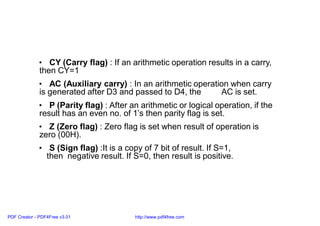
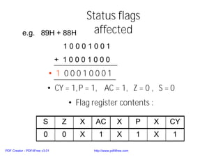
Download to read offline

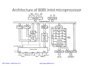

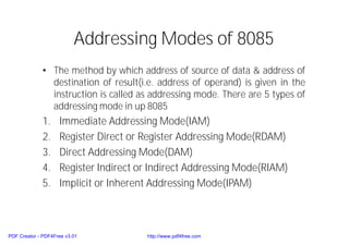
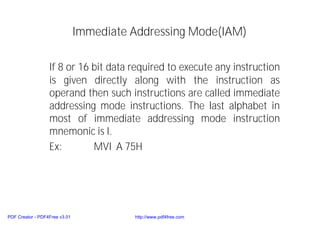
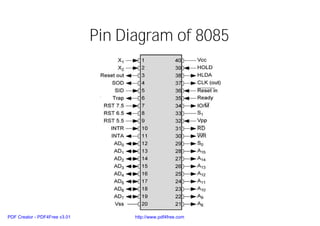
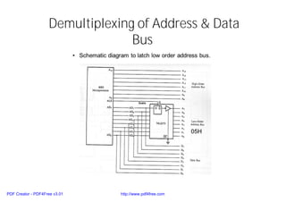

The document provides a detailed overview of the architecture and functionality of the 8085 Intel microprocessor, including descriptions of its functional units, flag register, addressing modes, and pin diagrams. Key components like the accumulator, program counter, and various registers are covered, along with their purposes in arithmetic and logical operations. It also details control signals for I/O and memory organization and explains the demultiplexing of the address and data bus.


![[Deck] What's New in Spark-Iceberg Integration via DSV2.pptx](https://cdn.slidesharecdn.com/ss_thumbnails/deckwhatsnewinspark-icebergintegrationviadsv2-260210005337-25955b12-thumbnail.jpg?width=640&height=640&fit=bounds)


