Downloaded 15 times


![DEC byte ;byte=byte-1
INC byte ;byte=byte+1
INC R7
DEC A
DEC 40H ; [40]=[40]-1](https://image.slidesharecdn.com/microcontroller8051-140823123204-phpapp01/85/Microcontroller-8051-37-320.jpg)


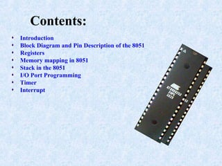
The document discusses different aspects of microprocessors and microcontrollers including hardware, software, common components like CPU, memory, I/O ports, and differences between microprocessors and microcontrollers. It provides block diagrams of a general microprocessor system and microcontroller with descriptions of each component. Examples given include the Intel 8051 microcontroller and its pin descriptions and registers.


