Maheshsavarala Specialization: PG-DIPLOMA in VLSI Design
Date of Birth: 5th june 1991 Contact details: +917204642760
Email: smahesh258@gmail.com
OBJECTIVES
Intend to build a career that broadens existing skills, which is completely devoted with sincere efforts towards the
growth of the organization.
PROFESSIONAL WORK EXPERIENCE:-
Summary: -
 Total of 3 years of experience in VLSI semiconductor industry in Physical Design. (2.4 yrs relevant)
 Worked on 3 successful tape outs at PMC-SIERRA and AMD with complete ownership of timingand
physical closure activities
 W orked on designs from Floorplan to GDSII
 Possess sound knowledge in PnR, Timing closure, PV and Tapeout.
 Worked on Physical Design of 16nm, 28 nm and 40 nm chips.
 Worked on low power design
 Good in TCL scripting.
Worked for PMC-SIERRA (Microsemi)
Project 1: - Worked on two Subsystem Level Timing and Physical closure in Innovus
Team: 5
Responsibility: Netlist to GDS implementation of block. It Included FloorPlan, PowerPlanning,
ClockTreeSynthesis(MPCTS), Routing, SPEF Extraction, Timing Analysis, Post ECO Fixing, DRC&LVS.
Details: - 28nm, 9Metal Layers
Challenges: -
 Worked on design with gate counts up to 1Million, operating frequency 501 MHz
 Worked on MCMM optimizations and Clock Tree Synthesis,worked on constraint cleanup
activities.
 Worked on complete Physical Verification for TSMC DRC and LVS closure.
 Implemented 35 clocks with max frequency being 501 MHz and achieved cross clock skew
balance.
 Implemented source synchronous interface to meet custom routing and skew requirement
between data and clock.
 Implemented power gating in block using precharge and header cells
Worked for AMD
Project 2: - Block P&R implementation.
Team: 6
Responsibility: Netlist to GDS implementation of block. It Included FloorPlan, Power
Planning, Clock Tree Synthesis(MPCTS),Routing,SPEF Extraction,Timing Analysis, PostECO Fixing,
DRC&LVS. Tools:ICCompiler,Encounter,StarRC,PTSI,Calibre,Conformal.
Block 1 Design Statistics: 7 macros, 1 primary Clock Max Frequency 909MHZ, 0.5M instances
Details: - 16nm, 11 Metal Layers
Challenges: -
 Timing critical Design, housing two PLL which generates multiple clocks.
 Built manual clock tree for few clocks (REFCLK, SYSCLK) to match skew requirements.
 Done shielding & custom Routing for clocks to reduce noise on clock nets.
TOOLS USED : -
 PD, Place and Route :Atoptech Aprisa, Cadence Innovus, ICC
 Extraction Tools : QRC
 Power Analysis : EPS
 LEC : Conformal
 STA : Primetime, Tweaker, Goldtime
 SI Analysis : PTSI, ETS
 Scripting Language : TCL
ACADEMICQUALIFICATIONS
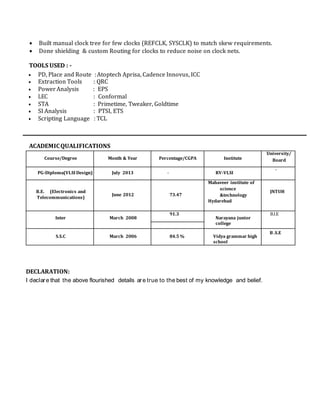
Course/Degree Month & Year Percentage/CGPA Institute
University/
Board
PG-Diploma(VLSI Design) July 2013 - RV-VLSI
-
B.E. (Electronics and
Telecommunications)
June 2012 73.47
Mahaveer institute of
science
&technology
Hydarebad
JNTUH
Inter March 2008
91.3
Narayana junior
college
B.I.E
S.S.C March 2006 84.5 % Vidya grammar high
school
B .S.E
DECLARATION:
I declare that the above flourished details are true to the best of my knowledge and belief.

Mahesh_Resume

  • 1.
    Maheshsavarala Specialization: PG-DIPLOMAin VLSI Design Date of Birth: 5th june 1991 Contact details: +917204642760 Email: smahesh258@gmail.com OBJECTIVES Intend to build a career that broadens existing skills, which is completely devoted with sincere efforts towards the growth of the organization. PROFESSIONAL WORK EXPERIENCE:- Summary: -  Total of 3 years of experience in VLSI semiconductor industry in Physical Design. (2.4 yrs relevant)  Worked on 3 successful tape outs at PMC-SIERRA and AMD with complete ownership of timingand physical closure activities  W orked on designs from Floorplan to GDSII  Possess sound knowledge in PnR, Timing closure, PV and Tapeout.  Worked on Physical Design of 16nm, 28 nm and 40 nm chips.  Worked on low power design  Good in TCL scripting. Worked for PMC-SIERRA (Microsemi) Project 1: - Worked on two Subsystem Level Timing and Physical closure in Innovus Team: 5 Responsibility: Netlist to GDS implementation of block. It Included FloorPlan, PowerPlanning, ClockTreeSynthesis(MPCTS), Routing, SPEF Extraction, Timing Analysis, Post ECO Fixing, DRC&LVS. Details: - 28nm, 9Metal Layers Challenges: -  Worked on design with gate counts up to 1Million, operating frequency 501 MHz  Worked on MCMM optimizations and Clock Tree Synthesis,worked on constraint cleanup activities.  Worked on complete Physical Verification for TSMC DRC and LVS closure.  Implemented 35 clocks with max frequency being 501 MHz and achieved cross clock skew balance.  Implemented source synchronous interface to meet custom routing and skew requirement between data and clock.  Implemented power gating in block using precharge and header cells Worked for AMD Project 2: - Block P&R implementation. Team: 6 Responsibility: Netlist to GDS implementation of block. It Included FloorPlan, Power Planning, Clock Tree Synthesis(MPCTS),Routing,SPEF Extraction,Timing Analysis, PostECO Fixing, DRC&LVS. Tools:ICCompiler,Encounter,StarRC,PTSI,Calibre,Conformal. Block 1 Design Statistics: 7 macros, 1 primary Clock Max Frequency 909MHZ, 0.5M instances Details: - 16nm, 11 Metal Layers Challenges: -  Timing critical Design, housing two PLL which generates multiple clocks.
  • 2.
     Built manualclock tree for few clocks (REFCLK, SYSCLK) to match skew requirements.  Done shielding & custom Routing for clocks to reduce noise on clock nets. TOOLS USED : -  PD, Place and Route :Atoptech Aprisa, Cadence Innovus, ICC  Extraction Tools : QRC  Power Analysis : EPS  LEC : Conformal  STA : Primetime, Tweaker, Goldtime  SI Analysis : PTSI, ETS  Scripting Language : TCL ACADEMICQUALIFICATIONS Course/Degree Month & Year Percentage/CGPA Institute University/ Board PG-Diploma(VLSI Design) July 2013 - RV-VLSI - B.E. (Electronics and Telecommunications) June 2012 73.47 Mahaveer institute of science &technology Hydarebad JNTUH Inter March 2008 91.3 Narayana junior college B.I.E S.S.C March 2006 84.5 % Vidya grammar high school B .S.E DECLARATION: I declare that the above flourished details are true to the best of my knowledge and belief.