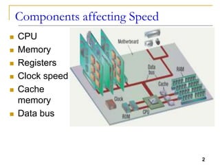
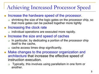
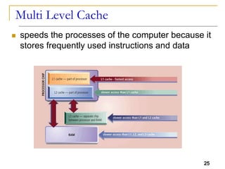
The document discusses various components that affect processor speed, including the CPU, memory, registers, clock speed, and cache memory. It describes how processor speed has been increased over time through shrinking components, increasing clock rates, optimizing cache sizes and speeds, and implementing parallelism. The document also discusses registers in detail, including their functions, sizes, and different types. It explains the role of the system clock and clock rate in governing processor operations. Finally, it covers cache memory hierarchies, bus architectures, and the functions of data, address and control buses.
intel core i7 is almost the best processor which is available in market.in many respect either of speed,concurrency increased cache ,QPI ,Hyper threading and many more!
1.CPU INSTRUCTION AND EXECUTION CYCLEThe primary function of the .pdfaniyathikitchen
1.CPU INSTRUCTION AND EXECUTION CYCLE:
The primary function of the cpu of a computer is to execute the sequence of instructions stored
ina memory which is an external to the cpu.The cpu must first fetch an instruction from the
memory before it can be executed .The sequence of operations involved in processing an
instruction constitutes an instruction cycle.This can be sub divided into two major phases i.e.,
fetch phase and execution phase.These two phases are performed in two cosecutive time slots
under the control of a clock.Hence these two operations are called as cycles .The time needed to
complete the execution of an instruction is known as INSTRUCTION CYCLE time .
a.FETCH CYCLE:The instruction is obtained from main memory during the fetch cycle.The
fetch operation can be described as \"send the address of the next instruction to memory and
recieve the instruction from the memory\".
b.EXECUTION CYCLE:The execution cycle includes decoding the instruction fetching of the
required operand and performing the operations specified by aninstructions opcode.In other
words it can be stated as \"Decode the fetched instruction if the operand is specified in the
memory then fetch that operand and execute the instruction \".
**INSTRUCTION CYCLE:
Thus the fetch and execute operations are carried out in synchronism with a clock is known as
instruction cycle i.e.,IC=FC+EC.
3.a.INSTUCTION FORMAT:Instruction format has one or more number of fields.The first field
is called as operation code field or opcode fielde which indicates type of operations to be
performed by the cpu.It also contains other fields known as operand fields.The cpu executes the
instructions using the information which resides in these fields.
b.WORD SIZE:A memory unit stores binary information in group of bits called words.The
number of bits in each word is often refered to as the WORD SIZE of a computer.Each word is
stored in one memory register.The word size in micro and mini computers ranges from 8 to 32
bits, and large computers usually have 32 or more bits in a word.
c.CLOCK RATE:A clock is a square wave , which is used to synchronize various devices in the
microprocessor and the system.Every microprocessor system requires a clock for its
functioning.The time taken for the microprocessor and the system to execute an instruction is
called clockrate.
4.FUNCTION OF GENERAL PURPOSE AND SPECIAL PURPOSE REGISTERS:
General purpose registers are available to store any transient data required by the program.For
example, when a program is interrupted its state, ie: the value of the registers such as the
program counter, instruction register or memory address register - may be saved into the general
purpose registers, ready for recall when the program is ready to start again.In general the more
registers a CPU has available, the faster it can work.
A Special Function Register (or Special Purpose Register, or simply Special Register) is a
register within a microprocessor, which controls or mon.
June 3, 2024 Anti-Semitism Letter Sent to MIT President Kornbluth and MIT Cor...Levi Shapiro
Letter from the Congress of the United States regarding Anti-Semitism sent June 3rd to MIT President Sally Kornbluth, MIT Corp Chair, Mark Gorenberg
Dear Dr. Kornbluth and Mr. Gorenberg,
The US House of Representatives is deeply concerned by ongoing and pervasive acts of antisemitic
harassment and intimidation at the Massachusetts Institute of Technology (MIT). Failing to act decisively to ensure a safe learning environment for all students would be a grave dereliction of your responsibilities as President of MIT and Chair of the MIT Corporation.
This Congress will not stand idly by and allow an environment hostile to Jewish students to persist. The House believes that your institution is in violation of Title VI of the Civil Rights Act, and the inability or
unwillingness to rectify this violation through action requires accountability.
Postsecondary education is a unique opportunity for students to learn and have their ideas and beliefs challenged. However, universities receiving hundreds of millions of federal funds annually have denied
students that opportunity and have been hijacked to become venues for the promotion of terrorism, antisemitic harassment and intimidation, unlawful encampments, and in some cases, assaults and riots.
The House of Representatives will not countenance the use of federal funds to indoctrinate students into hateful, antisemitic, anti-American supporters of terrorism. Investigations into campus antisemitism by the Committee on Education and the Workforce and the Committee on Ways and Means have been expanded into a Congress-wide probe across all relevant jurisdictions to address this national crisis. The undersigned Committees will conduct oversight into the use of federal funds at MIT and its learning environment under authorities granted to each Committee.
• The Committee on Education and the Workforce has been investigating your institution since December 7, 2023. The Committee has broad jurisdiction over postsecondary education, including its compliance with Title VI of the Civil Rights Act, campus safety concerns over disruptions to the learning environment, and the awarding of federal student aid under the Higher Education Act.
• The Committee on Oversight and Accountability is investigating the sources of funding and other support flowing to groups espousing pro-Hamas propaganda and engaged in antisemitic harassment and intimidation of students. The Committee on Oversight and Accountability is the principal oversight committee of the US House of Representatives and has broad authority to investigate “any matter” at “any time” under House Rule X.
• The Committee on Ways and Means has been investigating several universities since November 15, 2023, when the Committee held a hearing entitled From Ivory Towers to Dark Corners: Investigating the Nexus Between Antisemitism, Tax-Exempt Universities, and Terror Financing. The Committee followed the hearing with letters to those institutions on January 10, 202
Welcome to TechSoup New Member Orientation and Q&A (May 2024).pdfTechSoup
In this webinar you will learn how your organization can access TechSoup's wide variety of product discount and donation programs. From hardware to software, we'll give you a tour of the tools available to help your nonprofit with productivity, collaboration, financial management, donor tracking, security, and more.
Embracing GenAI - A Strategic ImperativePeter Windle
Artificial Intelligence (AI) technologies such as Generative AI, Image Generators and Large Language Models have had a dramatic impact on teaching, learning and assessment over the past 18 months. The most immediate threat AI posed was to Academic Integrity with Higher Education Institutes (HEIs) focusing their efforts on combating the use of GenAI in assessment. Guidelines were developed for staff and students, policies put in place too. Innovative educators have forged paths in the use of Generative AI for teaching, learning and assessments leading to pockets of transformation springing up across HEIs, often with little or no top-down guidance, support or direction.
This Gasta posits a strategic approach to integrating AI into HEIs to prepare staff, students and the curriculum for an evolving world and workplace. We will highlight the advantages of working with these technologies beyond the realm of teaching, learning and assessment by considering prompt engineering skills, industry impact, curriculum changes, and the need for staff upskilling. In contrast, not engaging strategically with Generative AI poses risks, including falling behind peers, missed opportunities and failing to ensure our graduates remain employable. The rapid evolution of AI technologies necessitates a proactive and strategic approach if we are to remain relevant.
The Roman Empire A Historical Colossus.pdfkaushalkr1407
The Roman Empire, a vast and enduring power, stands as one of history's most remarkable civilizations, leaving an indelible imprint on the world. It emerged from the Roman Republic, transitioning into an imperial powerhouse under the leadership of Augustus Caesar in 27 BCE. This transformation marked the beginning of an era defined by unprecedented territorial expansion, architectural marvels, and profound cultural influence.
The empire's roots lie in the city of Rome, founded, according to legend, by Romulus in 753 BCE. Over centuries, Rome evolved from a small settlement to a formidable republic, characterized by a complex political system with elected officials and checks on power. However, internal strife, class conflicts, and military ambitions paved the way for the end of the Republic. Julius Caesar’s dictatorship and subsequent assassination in 44 BCE created a power vacuum, leading to a civil war. Octavian, later Augustus, emerged victorious, heralding the Roman Empire’s birth.
Under Augustus, the empire experienced the Pax Romana, a 200-year period of relative peace and stability. Augustus reformed the military, established efficient administrative systems, and initiated grand construction projects. The empire's borders expanded, encompassing territories from Britain to Egypt and from Spain to the Euphrates. Roman legions, renowned for their discipline and engineering prowess, secured and maintained these vast territories, building roads, fortifications, and cities that facilitated control and integration.
The Roman Empire’s society was hierarchical, with a rigid class system. At the top were the patricians, wealthy elites who held significant political power. Below them were the plebeians, free citizens with limited political influence, and the vast numbers of slaves who formed the backbone of the economy. The family unit was central, governed by the paterfamilias, the male head who held absolute authority.
Culturally, the Romans were eclectic, absorbing and adapting elements from the civilizations they encountered, particularly the Greeks. Roman art, literature, and philosophy reflected this synthesis, creating a rich cultural tapestry. Latin, the Roman language, became the lingua franca of the Western world, influencing numerous modern languages.
Roman architecture and engineering achievements were monumental. They perfected the arch, vault, and dome, constructing enduring structures like the Colosseum, Pantheon, and aqueducts. These engineering marvels not only showcased Roman ingenuity but also served practical purposes, from public entertainment to water supply.
The French Revolution, which began in 1789, was a period of radical social and political upheaval in France. It marked the decline of absolute monarchies, the rise of secular and democratic republics, and the eventual rise of Napoleon Bonaparte. This revolutionary period is crucial in understanding the transition from feudalism to modernity in Europe.
For more information, visit-www.vavaclasses.com
Biological screening of herbal drugs: Introduction and Need for
Phyto-Pharmacological Screening, New Strategies for evaluating
Natural Products, In vitro evaluation techniques for Antioxidants, Antimicrobial and Anticancer drugs. In vivo evaluation techniques
for Anti-inflammatory, Antiulcer, Anticancer, Wound healing, Antidiabetic, Hepatoprotective, Cardio protective, Diuretics and
Antifertility, Toxicity studies as per OECD guidelines
Synthetic Fiber Construction in lab .pptxPavel ( NSTU)
Synthetic fiber production is a fascinating and complex field that blends chemistry, engineering, and environmental science. By understanding these aspects, students can gain a comprehensive view of synthetic fiber production, its impact on society and the environment, and the potential for future innovations. Synthetic fibers play a crucial role in modern society, impacting various aspects of daily life, industry, and the environment. ynthetic fibers are integral to modern life, offering a range of benefits from cost-effectiveness and versatility to innovative applications and performance characteristics. While they pose environmental challenges, ongoing research and development aim to create more sustainable and eco-friendly alternatives. Understanding the importance of synthetic fibers helps in appreciating their role in the economy, industry, and daily life, while also emphasizing the need for sustainable practices and innovation.
3. 3
Achieving Increased Processor Speed
Increase the hardware speed of the processor.
shrinking the size of the logic gates on the processor chip, so
that more gates can be packed together more tightly
Increasing the clock rate
individual operations are executed more rapidly.
Increase the size and speed of caches
In particular, by dedicating a portion of the processor chip
itself to the cache,
cache access times drop significantly.
Make changes to the processor organization and
architecture that increase the effective speed of
instruction execution.
Typically, this involves using parallelism in one form or
another.
3
4. 4
Registers
processor contains small, high-speed storage
locations
temporarily hold data and instructions
part of the processor, not part of memory or a
permanent storage device.
Different types of registers, each with a specific
storage function including
storing the location from where an instruction was
fetched
storing an instruction while the control unit decodes it
storing data while the ALU computes it, and
storing the results of a calculation.
4
5. 5
Register Function
Almost all computers load data from a larger
memory into registers where it is used for
arithmetic,
manipulated, or
tested, by some machine instruction.
Manipulated data is then often stored back in
main memory,
either by the same instruction or
a subsequent one.
5
6. 6
Register Size
Number of bits processor can handle
Word size
indicates the amount of data with which the
computer can work at any given time
Larger indicates more powerful computer
Increase by purchasing new CPU
16 bit registers
32 bit registers
64 bit registers
6
7. 7
User Accessible Registers
Data registers
can hold numeric values such as integer and
floating-point values, as well as characters, small bit
arrays and other data.
In some older CPUs, a special data register
accumulator, is used implicitly for many operations.
Address registers
hold addresses and are used by instructions that
indirectly access main memory i.e. RAM
7
8. 8
Other types of Registers
Conditional registers
hold truth values often used to determine whether some
instruction should or should not be executed.
General purpose registers (GPRs)
can store both data and addresses, i.e., they are
combined Data/Address registers.
Floating point registers (FPRs)
store floating point numbers in many architectures.
Constant registers
hold read-only values such as zero, one, or pi.
Vector registers
hold data for vector processing done by SIMD
instructions (Single Instruction, Multiple Data).
8
9. 9
Other types of Registers
Control and Status registers hold program state; they
usually include
Program counter (aka instruction pointer) and
Status register (aka processor status word or Flag register).
Instruction register store the instruction currently being
executed
Registers related to fetching information from RAM,
Memory Buffer register (MBR)
Memory Data register (MDR)
Memory Address register (MAR)
Memory Type Range Registers (MTRR)
Hardware registers are similar, but occur outside
CPUs.
9
10. 10
System or Internal Clock
Operations performed by a processor, such as
fetching an instruction,
decoding the instruction,
performing an arithmetic operation, and so on,
are governed by a system clock
Typically, all operations begin with the pulse of the
clock
Speed of a processor is dictated by the pulse frequency
produced by the clock, measured in cycles per second,
or Hertz (Hz)
Clock signals are generated by a quartz crystal, which
generates a constant signal wave while power is
applied.
This wave is converted into a digital voltage pulse stream that
is provided in a constant flow to the processor circuitry
10
11. 11
System or Internal Clock
The rate of pulses is known as the clock rate, or
clock speed.
One increment, or pulse, of the clock is referred to
as a clock cycle, or a clock tick or the time it
takes to turn a transistor off and back on again.
The time between pulses is the cycle time.
controls the timing of all computer operations
A processor can execute an instruction in a given
number of clock cycles.
Pace of the system clock is called the clock speed
Modern machines use Giga Hertz (GHz)
One billion clock ticks in one second
11
12. 12
Underclocking and Overclocking
Underclocking
With any particular CPU, replacing the crystal with
another crystal that oscillates half the frequency will
generally make the CPU run at half the performance
and reduce waste heat produced by the CPU.
Overclocking
to increase performance of a CPU by replacing the
oscillator crystal with a higher frequency crystal
the amount of overclocking is limited by the time for
the CPU to settle after each pulse, and by the extra
heat created.
12
13. 13
Overclocking
process of making a computer or component
operate faster than specified by the manufacturer by
modifying system parameters.
Most overclocking techniques increase power
consumption, generating more heat, which must be
carried away.
The purpose of overclocking is to increase the
operating speed of given hardware.
Computer components that may be overclocked
include
processors (CPU),
video cards,
motherboard chipsets, and
RAM.
13
14. 14
Cache Function
The data that is stored within a cache
might be values that have been computed earlier or
duplicates of original values that are stored elsewhere
If requested data is contained in the cache (cache
hit),
this request can be served by simply reading the cache,
which is comparatively faster.
Otherwise (cache miss),
the data has to be recomputed or fetched from its original
storage location, which is comparatively slower.
Hence, the greater the number of requests that can
be served from the cache, the faster the overall
system performance becomes.
15. 15
Cache
Small amount of very fast memory which stores
copies of the data from the most frequently used
main memory locations
Sits between normal main memory (RAM & ROM)
and CPU
May be located on CPU chip or module
Used to reduce the average time to access
memory.
As long as most memory accesses are cached
memory locations, the average access time of
memory accesses will be closer to the cache
access time than to the access time of main
memory.
16. 16
Cache Operation – Overview
CPU requests contents of memory location
Check cache for this data
If present, get from cache (fast)
If not present, read required block from main
memory to cache
Then deliver from cache to CPU
Cache includes tags to identify which block of
main memory is in each cache slot
18. 18
Types of Cache
Most modern desktop and server CPUs have
at least three independent caches:
an instruction cache to speed up executable
instruction fetch,
a data cache to speed up data fetch and store,
and
a translation lookaside buffer (TLB) used to
speed up virtual-to-physical address translation
for both executable instructions and data.
19. 19
Multi Level Cache
Another issue is the fundamental tradeoff between
cache access time and hit rate
Larger caches have better hit rates but longer access time
To address this tradeoff, many computers use multiple
levels of cache, with small fast caches backed up by
larger slower caches.
Multi-level caches generally operate by checking the
smallest level 1 (L1) cache first;
if it hits, the processor proceeds at high speed.
If the smaller cache misses, the next larger cache (L2) is
checked, and
so on, before external memory is checked.
L1 holds recently used data
L2 holds upcoming data
L3 holds possible upcoming data
19
20. 20
Multilevel Caches
High logic density enables caches on chip
Faster than bus access
Frees bus for other transfers
Common to use both on and off chip cache
L1 on chip, L2 off chip in static RAM
L2 access much faster than DRAM or ROM
L2 often uses separate data path
L2 may now be on chip
Resulting in L3 cache
Bus access or now on chip…
22. 22
L1 Cache
Built directly in the processor chip.
Usually has a very small capacity, ranging from
8 KB to 128 KB.
The more common sizes for PCs are 32 KB or
64 KB.
23. 23
L2 Cache
Slightly slower than L1 cache
Has a much larger capacity, ranging from 64
KB to 16 MB
Current processors include Advanced Transfer
Cache (ATC), a type of L2 cache built directly
on the processor chip
Processors that use ATC perform at much
faster rates than those that do not use it
PCs today have from 512 KB to 12 MB of ATC
Servers and workstations have from 12 MB to
16 MB of ATC
24. 24
L3 Cache
L3 cache is a cache on the motherboard
Separate from the processor chip.
Exists only on computers that use L2
Advanced Transfer Cache.
Personal computers often have up to 8 MB of
L3 cache;
Servers and work stations have from 8 MB to
24 MB of L3 cache.
25. 25
Multi Level Cache
speeds the processes of the computer because it
stores frequently used instructions and data
25
26. 26
Intel Cache Evolution
Problem Solution
Processor on which
feature first appears
External memory slower than the system bus.
Add external cache using
faster memory technology.
386
Increased processor speed results in external
bus becoming a bottleneck for cache access.
Move external cache on-
chip, operating at the same
speed as the processor.
486
Internal cache is rather small, due to limited
space on chip
Add external L2 cache using faster
technology than main memory
486
Contention occurs when both the Instruction
Prefetcher and the Execution Unit simultaneously
require access to the cache. In that case, the
Prefetcher is stalled while the Execution Unit’s data
access takes place.
Create separate data and
instruction caches.
Pentium
Increased processor speed results in external
bus becoming a bottleneck for L2 cache
access.
Create separate back-side bus that
runs at higher speed than the main
(front-side) external bus. The BSB
is dedicated to the L2 cache.
Pentium Pro
Move L2 cache on to the
processor chip.
Pentium II
Some applications deal with massive
databases and must have rapid access to large
amounts of data. The on-chip caches are too
small.
Add external L3 cache. Pentium III
Move L3 cache on-chip. Pentium 4
27. 27
Memory hierarchy –Design constraints
How much?
open ended. If the capacity is there, applications will
likely be developed to use it
How fast?
To achieve greatest performance, the memory must
be able to keep up with the processor.
As the processor is executing instructions, it should not
have to pause waiting for instructions or operands.
How expensive?
the cost of memory must be reasonable in
relationship to other components
28. 28
Memory Hierarchy
28
Faster access time,
greater cost per bit
Greater capacity, smaller
cost per bit
Greater capacity, slower
access time
31. 31
Virtual RAM
Computer is out of actual
RAM
File that emulates RAM
Computer swaps data to
virtual RAM
Least recently used data is
moved
Techniques
Paging
Segmentation or
Combination of both
31
32. 32
The Bus
Electronic pathway between components
Two main buses: Internal (or system) bus and
External (or expansion) bus.
Internal or System bus
resides on the motherboard and connects the CPU to
other devices that reside on the motherboard
has three parts: the data bus, address bus and control
bus
External or Expansion bus
connects external devices, such as the keyboard,
mouse, modem, printer and so on, to the CPU.
Cables from disk drives and other internal devices are
plugged into the bus.
32
33. 33
Bus Width and Speed
Bus width is measured in bits
Speed is tied to the clock
33
35. 35
Data Bus
is a computer subsystem that allows for the
transferring of data
from one component to another on a motherboard or system
board, or
between two computers.
This can include transferring data to and from the
memory, or from CPU to other components
Each one is designed to handle so many bits of data
at a time.
The amount of data a data bus can handle is called
bandwidth
A typical data bus is 32-bits wide
Newer computers are making data buses that can
handle 64-bit
35
36. 36
Address Bus
is a series of lines connecting two or more devices
that is used to specify a physical address.
When a processor needs to read or write to a
memory location,
it specifies that memory location on the address bus (the
value to be read or written is sent on the data bus).
The width of the address bus determines the
amount of memory a system can address.
For example, a system with a 32-bit address bus can
address 232 (4,294,967,296) memory locations.
If each memory address holds one byte, the addressable
memory space is 4 GB.
36
37. 37
Control Bus
A control bus is (part of) a computer bus, used
by CPUs for communicating with other devices
within the computer.
While the address bus carries the information on
which device the CPU is communicating with and
data bus carries the actual data being processed,
Control bus carries commands from the CPU
and returns status signals from the devices
e.g. if the data is being read or written to the device
the appropriate line (read or write) will be active
37
38. 38
Summary I
Components Affecting Speed
Achieving Increased Processor Speed
Registers
Functions and Size
User accessible and other types of Registers
System or Internal Clock
Clock speed and clock rate
Underclocking
Overclocking
39. 39
Summary II
Cache memory
Function operation
Type: Instruction, data and TLB
Multi Level Cache, L1, L2 and L3
Intel Cache Evolution
Memory Hierarchy
Bus
Bus width and speed
Bus Interconnection Scheme
Data, address and control bus