1. How a CPU Works
Introduction
Even though every microprocessor has its own internal design, all microprocessors share a
same basic concept – which we will explain in this tutorial. We will take a look inside a
generic CPU architecture, so you will be able to understand more about Intel and AMD
products and the differences between them.
The CPU (Central Processing Unit) – which is also called microprocessor or processor – is
in charge of processing data. How it will process data will depend on the program. The
program can be a spreadsheet, a word processor or a game: for the CPU it makes no
difference, since it doesn’t understand what the program is actually doing. It just follows
the orders (called commands or instructions) contained inside the program. These orders
could be to add two numbers or to send a piece of data to the video card, for example.
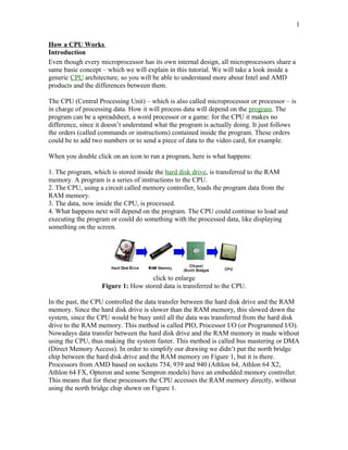
When you double click on an icon to run a program, here is what happens:
1. The program, which is stored inside the hard disk drive, is transferred to the RAM
memory. A program is a series of instructions to the CPU.
2. The CPU, using a circuit called memory controller, loads the program data from the
RAM memory.
3. The data, now inside the CPU, is processed.
4. What happens next will depend on the program. The CPU could continue to load and
executing the program or could do something with the processed data, like displaying
something on the screen.
click to enlarge
Figure 1: How stored data is transferred to the CPU.
In the past, the CPU controlled the data transfer between the hard disk drive and the RAM
memory. Since the hard disk drive is slower than the RAM memory, this slowed down the
system, since the CPU would be busy until all the data was transferred from the hard disk
drive to the RAM memory. This method is called PIO, Processor I/O (or Programmed I/O).
Nowadays data transfer between the hard disk drive and the RAM memory in made without
using the CPU, thus making the system faster. This method is called bus mastering or DMA
(Direct Memory Access). In order to simplify our drawing we didn’t put the north bridge
chip between the hard disk drive and the RAM memory on Figure 1, but it is there.
Processors from AMD based on sockets 754, 939 and 940 (Athlon 64, Athlon 64 X2,
Athlon 64 FX, Opteron and some Sempron models) have an embedded memory controller.
This means that for these processors the CPU accesses the RAM memory directly, without
using the north bridge chip shown on Figure 1.
1
2. Clock
So, what is clock anyway? Clock is a signal used to sync things inside the computer. Take a
look on Figure 2, where we show a typical clock signal: it is a square wave changing from
“0” to “1” at a fixed rate. On this figure you can see three full clock cycles (“ticks”). The
beginning of each cycle is when the clock signal goes from “0” to “1”; we marked this with
an arrow. The clock signal is measured in a unit called Hertz (Hz), which is the number of
clock cycles per second. A clock of 100 MHz means that in one second there is 100 million
clock cycles.
Figure 2: Clock signal.
In the computer, all timings are measured in terms of clock cycles. For example, a RAM
memory with a “5” latency means that it will delay five full clock cycles to start delivering
data. Inside the CPU, all instructions delay a certain number of clock cycles to be
performed. For example, a given instruction can delay seven clock cycles to be fully
executed.
Regarding the CPU, the interesting thing is that the CPU knows how many clock cycles
each instruction will take, because it has a table which lists this information. So if it has two
instructions to be executed and it knows that the first will delay seven clock cycles to be
executed, it will automatically start the execution of the next instruction on the 8th clock
tick. Of course this is a generic explanation for a CPU with just one execution unit –
modern processors have several execution units working in parallel and it could execute the
second instruction at the same time as the first, in parallel. This is called superscalar
architecture and we will talk more about this later.
So, what clock has to do with performance? To think that clock and performance is the
same thing is the most common misconception about processors.
If you compare two completely identical CPUs, the one running at a higher clock rate will
be faster. In this case, with a higher clock rate, the time between each clock cycle will be
shorter, so things are going to be performed in less time and the performance will be higher.
But when you do compare two different processors, this is not necessarily true.
If you get two processors with different architectures – for example, two different
manufacturers, like Intel and AMD – things inside the CPU are completely different.
As we mentioned, each instruction takes a certain number of clock cycles to be executed.
Let’s say that processor “A” takes seven clock cycles to perform a given instruction, and
that processor “B” takes five clock cycles to perform this same instruction. If they are
running at the same clock rate, processor “B” will be faster, because it can process this
2
3. instruction is less time.
For modern CPUs there is much more in the performance game, as CPUs have different
number of execution units, different cache sizes, different ways of transferring data inside
the CPU, different ways of processing the instructions inside the execution units, different
clock rates with the outside world, etc. Don’t worry; we will cover all that in this tutorial.
As the processor clock signal became very high, one problem showed up. The motherboard
where the processor is installed could not work using the same clock signal. If you look at a
motherboard, you will see several tracks or paths. These tracks are wires that connect the
several circuits of the computer. The problem is that with higher clock rates, these wires
started to work as antennas, so the signal, instead of arriving at the other end of the wire,
would simply vanish, being transmitted as radio waves.
Figure 3: The wires on the motherboard can work as antennas.
External Clock
So the CPU manufacturers started using a new concept, called clock multiplication, which
started with 486DX2 processor. Under this scheme, which is used in all CPUs nowadays,
the CPU has an external clock, which is used when transferring data to and from the RAM
memory (using the north bridge chip), and a higher internal clock.
To give a real example, on a 3.4 GHz Pentium 4 this “3.4 GHz” refers to the CPU internal
clock, which is obtained multiplying by 17 its 200 MHz external clock. We illustrated this
example on Figure 4.
3
4. click to enlarge
Figure 4: Internal and external clocks on a Pentium 4 3.4 GHz.
The huge difference between the internal clock and the external clock on modern CPUs is
one major roadblock to overcome in order to increase the computer performance.
Continuing the Pentium 4 3.4 GHz example, it has to reduce its speed by 17x when it has to
read data from RAM memory! During this process, it works as if it were a 200 MHz CPU!
Several techniques are used to minimize the impact of this clock difference. One of them is
the use of a memory cache inside the CPU. Another one is transferring more than one data
chunk per clock cycle. Processors from both AMD and Intel use this feature, but while
AMD CPUs transfer two data per clock cycle, Intel CPUs transfer four data per clock cycle.
Figure 5: Transferring more than one data per clock cycle.
Because of that, AMD CPUs are listed as having the double of their real external clocks.
For example, an AMD CPU with a 200 MHz external clock is listed as 400 MHz. The same
happens with Intel CPUs: an Intel CPU with a 200 MHz external clock is listed as having
an 800 MHz external clock.
The technique of transferring two data per clock cycle is called DDR (Dual Data Rate),
while the technique of transferring four data per clock cycle is called QDR (Quad Data
Rate).
Block Diagram of a CPU
On Figure 6 you can see a basic block diagram for a modern CPU. There are many
differences between AMD and Intel architectures(read Inside Pentium 4 Architecture for a
4
5. detailed view on Pentium 4 architecture). Understanding the basic block diagram of a
modern CPU is the first step to understand how CPUs from Intel and AMD work and the
differences between them.
Figure 6: Basic block diagram of a CPU.
The dotted line on Figure 6 represents the CPU body, as the RAM memory is located
outside the CPU. The datapath between the RAM memory and the CPU is usually 64-bit
wide (or 128-bit when dual channel memory configuration is used), running at the memory
clock or the CPU external clock, which one is lower. The number of bits used and the clock
rate can be combined in a unit called transfer rate, measured in MB/s. To calculate the
transfer rate, the formula is number of bits x clock / 8. For a system using DDR400
memories in single channel configuration (64 bits) the memory transfer rate will be 3,200
MB/s, while the same system using dual channel memories (128 bits) will have a 6,400
MB/s memory transfer rate.
All the circuits inside the dotted box run at the CPU internal clock. Depending on the CPU
some of its internal parts can even run at a higher clock rate. Also, the datapath between the
CPU units can be wider, i.e. transfer more bits per clock cycle than 64 or 128. For example,
the datapath between the L2 memory cache and the L1 instruction cache on modern
processors is usually 256-bit wide. The higher the number the bits transferred per clock
cycle, the fast the transfer will be done (in other words, the transfer rate will be higher). On
Figure 6 we used a red arrow between the RAM memory and the L2 memory cache and
green arrows between all other blocks to express the different clock rates and datapath
width used.
Memory Cache
Memory cache is a high performance kind of memory, also called static memory. The kind
5
6. of memory used on the computer main RAM memory is called dynamic memory. Static
memory consumes more power, is more expensive and is physically bigger than dynamic
memory, but it is a lot faster. It can work at the same clock as the CPU, which dynamic
memory is not capable of.
Since going to the “external world” to fetch data makes the CPU to work at a lower clock
rate, memory cache technique is used. When the CPU loads a data from a certain memory
position, a circuit called memory cache controller (not drawn on Figure 6 in the name of
simplicity) loads into the memory cache a whole block of data below the current position
that the CPU has just loaded. Since usually programs flow in a sequential way, the next
memory position the CPU will request will probably be the position immediately below the
memory position that it has just loaded. Since the memory cache controller already loaded a
lot of data below the first memory position read by the CPU, the next data will be inside the
memory cache, so the CPU doesn’t need to go outside to grab the data: it is already loaded
inside in the memory cache embedded in the CPU, which it can access at its internal clock
rate.
The cache controller is always observing the memory positions being loaded and loading
data from several memory positions after the memory position that has just been read. To
give you a real example, if the CPU loaded data stored in the address 1,000, the cache
controller will load data from “n” addresses after the address 1,000. This number “n” is
called page; if a given processor is working with 4 KB pages (which is a typical value), it
will load data from 4,096 addresses below the current memory position being load (address
1,000 in our example). By the way, 1 KB equals to 1,024 bytes, that’s why 4 KB is 4,096
not 4,000. On Figure 7 we illustrate this example.
Figure 7: How the memory cache controller works.
The bigger the memory cache, the higher the chances of the data required by the CPU are
already there, so the CPU will need to directly access RAM memory less often, thus
increasing the system performance (just remember that every time the CPU needs to access
6
7. the RAM memory directly it needs to lower its clock rate for this operation).
We call a “hit” when the CPU loads a required data from the cache, and we call a “miss” if
the required data isn’t there and the CPU needs to access the system RAM memory.
L1 and L2 means “Level 1” and “Level 2”, respectively, and refers to the distance they are
from the CPU core (execution unit). One common doubt is why having three separated
cache memories (L1 data cache, L1 instruction cache and L2 cache). Pay attention to Figure
6 and you will see that L1 instruction cache works as an “input cache”, while L1 data cache
works as an “output cache”. L1 instruction cache – which is usually smaller than L2 cache
– is particularly efficient when the program starts to repeat a small part of it (loop), because
the required instructions will be closer to the fetch unit.
On the specs page of a CPU the L1 cache can be found with different kinds of
representation. Some manufacturers list the two L1 cache separately (some times calling
the instruction cache as “I” and the data cache as “D”), some add the amount of the two and
writes “separated” – so a “128 KB, separated” would mean 64 KB instruction cache and 64
KB data cache –, and some simply add the two and you have to guess that the amount is
total and you should divide by two to get the capacity of each cache. The exception,
however, goes to the Pentium 4 and newer Celeron CPUs based on sockets 478 and 775.
Pentium 4 processors (and Celeron processors using sockets 478 and 775) don’t have a L1
instruction cache, instead they have a trace execution cache, which is a cache located
between the decode unit and the execution unit. So, the L1 instruction cache is there, but
with a different name and a different location. We are mentioning this here because this is a
very common mistake, to think that Pentium 4 processors don’t have L1 instruction cache.
So when comparing Pentium 4 to other CPUs people would think that its L1 cache is much
smaller, because they are only counting the 8 KB L1 data cache. The trace execution cache
of Pentium 4 and Celeron CPUs is of 150 KB and should be taken in account, of course.
Branching
As we mentioned several times, one of the main problems for the CPU is having too many
cache misses, because the fetch unit must access directly the slow RAM memory, thus
slowing down the system.
Usually the use of the memory cache avoids this a lot, but there is one typical situation
where the cache controller will miss: branches. If in the middle of the program there is an
instruction called JMP (“jump” or “go to”) sending the program to a completely different
memory position, this new position won’t be loaded in the L2 memory cache, making the
fetch unit to go get that position directly in the RAM memory. In order to solve this issue,
the cache controller of modern CPUs analyze the memory block it loaded and whenever it
finds a JMP instruction in there it will load the memory block for that position in the L2
memory cache before the CPU reaches that JMP instruction.
7
8. Figure 8: Unconditional branching situation.
This is pretty easy to implement, the problem is when the program has a conditional
branching, i.e. the address the program should go to depends on a condition not yet known.
For example, if a =< b go to address 1, or if a > b go to address 2. We illustrate this
example on Figure 9. This would make a cache miss, because the values of a and b are
unknown and the cache controller would be looking only for JMP-like instructions. The
solution: the cache controller loads both conditions into the memory cache. Later, when the
CPU processes the branching instruction, it will simply discard the one that wasn’t chosen.
It is better to load the memory cache with unnecessary data than directly accessing the
RAM memory.
Figure 9: Conditional branching situation.
Processing Instructions
The fetch unit is in charge of loading instructions from memory. First, it will look if the
8
9. instruction required by the CPU is in the L1 instruction cache. If it is not, it goes to the L2
memory cache. If the instruction is also not there, then it has to directly load from the slow
system RAM memory.
When you turn on your PC all the caches are empty, of course, but as the system starts
loading the operating system, the CPU starts processing the first instructions loaded from
the hard drive, and the cache controller starts loading the caches, and the show begins.
After the fetch unit grabbed the instruction required by the CPU to be processed, it sends it
to the decode unit.
The decode unit will then figure out what that particular instruction does. It does that by
consulting a ROM memory that exists inside the CPU, called microcode. Each instruction
that a given CPU understands has its own microcode. The microcode will “teach” the CPU
what to do. It is like a step-by-step guide to every instruction. If the instruction loaded is,
for example, add a+b, its microcode will tell the decode unit that it needs two parameters, a
and b. The decode unit will then request the fetch unit to grab the data present in the next
two memory positions, which fit the values for a and b. After the decode unit “translated”
the instruction and grabbed all required data to execute the instruction, it will pass all data
and the “step-by-step cookbook” on how to execute that instruction to the execute unit.
The execute unit will finally execute the instruction. On modern CPUs you will find more
than one execution unit working in parallel. This is done in order to increase the processor
performance. For example, a CPU with six execution units can execute six instructions in
parallel, so in theory it could achieve the same performance of six processors with just one
execution unit. This kind of architecture is called superscalar architecture.
Usually modern CPUs don’t have several identical execution units; they have execution
units specialized in one kind of instructions. The best example is the FPU, Float Point Unit,
which is in charge of executing complex math instructions. Usually between the decode
unit and the execution unit there is an unit (called dispatch or schedule unit) in charge of
sending the instruction to the correct execution unit, i.e. if the instruction is a math
instruction it will send it to the FPU and not to one “generic” execution unit. By the way,
“generic” execution units are called ALU, Arithmetic and Logic Unit.
Finally, when the processing is over, the result is sent to the L1 data cache. Continuing our
add a+b example, the result would be sent to the L1 data cache. This result can be then sent
back to RAM memory or to another place, as the video card, for example. But this will
depend on the next instruction that is going to be processed next (the next instruction could
be “print the result on the screen”).
Another interesting feature that all microprocessors have for a long time is called
“pipeline”, which is the capability of having several different instructions at different stages
of the CPU at the same time.
After the fetch unit sent the instruction to the decode unit, it will be idle, right? So, how
9
10. about instead of doing nothing, put the fetch unit to grab the next instruction? When the
first instruction goes to the execution unit, the fetch unit can send the second instruction to
the decode unit and grab the third instruction, and so on.
In a modern CPU with an 11-stage pipeline (stage is another name for each unit of the
CPU), it will probably have 11 instructions inside it at the same time almost all the time. In
fact, since all modern CPUs have a superscalar architecture, the number of instructions
simultaneously inside the CPU will be even higher.
Also, for an 11-stage pipeline CPU, an instruction to be fully executed will have to pass
thru 11 units. The higher the number of stages, the higher the time an instruction will delay
to be fully executed. On the other hand, keep in mind that because of this concept several
instructions can be running inside the CPU at the same time. The very first instruction
loaded by the CPU can delay 11 steps to get out of it, but once it goes out, the second
instruction will get out right after it (and not another 11 steps later).
There are several other tricks used by modern CPUs to increase performance. We will
explain two of them, out-of-order execution (OOO) and speculative execution.
Out-Of-Order Execution (OOO)
Remember that we said that modern CPUs have several execution units working in
parallel? We also said that there are different kinds of execution units, like ALU, which is a
generic execution unit, and FPU, which is a math execution unit. Just as a generic example
in order to understand the problem, let’s say that a given CPU has six execution engines,
four “generic” and two FPUs. Let’s also say that the program has the following instruction
flow in a given moment:
1. generic instruction
2. generic instruction
3. generic instruction
4. generic instruction
5. generic instruction
6. generic instruction
7. math instruction
8. generic instruction
9. generic instruction
10. math instruction
What will happen? The schedule/dispatch unit will send the first four instructions to the
four ALUs but then, at the fifth instruction, the CPU will need to wait for one of their
ALUs to be free in order to continue processing, since all its four generic execution units
are busy. That’s not good, because we still have two math units (FPUs) available, and they
are idle. So, a CPU with out-of-order execution (all modern CPUs have this feature) will
look at the next instruction to see if it can be sent to one of the idle units. In our example, it
can’t, because the sixth instruction also needs one ALU to be processed. The out-of-order
10
11. engine continues its search and finds out that the seventh instruction is a math instruction
that can be executed in one of the available FPUs. Since the other FPU will still be
available, it will go down the program looking for another math instruction. In our
example, it will pass the eight and the ninth instructions and will load the tenth instruction.
So, in our example, the execution units will be processing, at the same time, the first, the
second, the third, the fourth, the seventh and the tenth instructions.
The name out-of-order comes from the fact that the CPU doesn’t need to wait; it can pull an
instruction from the bottom of the program and process it before the instructions above it
are processed. Of course the out-of-order engine cannot go forever looking for an
instruction if it cannot find one. The out-of-order engine of all CPUs has a depth limit on
which it can crawl looking for instructions (a typical value would be 512).
Speculative Execution
Let’s suppose that one of this generic instructions is a conditional branching. What will the
out-of-order engine do? If the CPU implements a feature called speculative execution (all
modern CPUs do), it will execute both branches. Consider the example below:
1. generic instruction
2. generic instruction
3. if a=<b go to instruction 15
4. generic instruction
5. generic instruction
6. generic instruction
7. math instruction
8. generic instruction
9. generic instruction
10. math instruction
…
15. math instruction
16. generic instruction
…
When the out-of-order engine analyses this program, it will pull instruction 15 into one of
the FPUs, since it will need one math to fill one of the FPUs that otherwise would be idle.
So at a given moment we could have both branches being processed at the same time. If
when the CPU finishes processing the third instruction a is greater than b, the CPU will
simple discard the processing of instruction 15. You may think this is a waste of time, but
in fact it is not. It doesn’t cost anything to the CPU to execute that particular instruction,
because the FPU would be otherwise idle anyway. On the other hand, if a=<b the CPU will
have a performance boost, since when instruction 3 asks for instruction 15 it will be already
processed, going straight to instruction 16 or even further, if instruction 16 has also already
been processed by the out-of-order engine.
11
12. Of course everything we explained on this tutorial is an over simplification in order to
make this very technical subject easier to understand.(read Inside Pentium 4 Architecture in
order to study the architecture of a specific processor).
Inside Pentium 4 Architecture
Introduction
In this tutorial we will explain you how Pentium 4 works in an easy to follow language.
You will learn exactly how its architecture works so you will be able to compare it more
precisely to previous processors from Intel and competitors from AMD.
Pentium 4 and new Celeron processors use Intel’s seventh generation architecture, also
called Netburst. Its overall look you can see on Figure 1. Don’t get scared. We will explain
deeply what this diagram is about.
In order to continue, however, you need to have read “How a CPU Works”.Ther we explain
the basics about how a CPU works. In the present tutorial we are assuming that you have
already read it, so if you didn’t, please take a moment to read it before continuing,
otherwise you may find yourself a little bit lost.
Figure 1: Pentium 4 block diagram.
Here are the basic differences between Pentium 4 architecture and the architecture from
other CPUs:
12
13. • Externally, Pentium 4 transfers four data per clock cycle. This technique is called
QDR (Quad Data Rate) and makes the local bus to have a performance four times
its actual clock rate, see table below. On Figure 1 this is shown on “3.2 GB/s
System Interface”; since this slide was produced when the very first Pentium 4 was
released, it mentions the “400 MHz” system bus.
●
Real Clock Performance Transfer Rate
100 MHz 400 MHz 3.2 GB/s
133 MHz 533 MHz 4.2 GB/s
200 MHz 800 MHz 6.4 GB/s
266 MHz 1,066 MHz 8.5 GB/s
• The datapath between the L2 memory cache (“L2 cache and control” on Figure 1)
and L1 data cache (“L1 D-Cache and D-TLB” on Figure 1) is 256-bit wide. On
previous processors from Intel this datapath was of only 64 bits. So this
communication can be four times faster than processors from previous generations
when running at the same clock. The datapath between L2 memory cache (“L2
cache and control” on Figure 1) and the pre-fetch unit (“BTB & I-TLB” on Figure
1), however, continues to be 64-bit wide.
• The L1 instruction cache was relocated. Instead of being before the fetch unit, the
L1 instruction cache is now after the decode unit, with a new name, “Trace Cache”.
This trace cache can hold up to 12 K microinstructions. Since each microinstruction
is 100-bit wide, the trace cache is of 150 KB (12 K x 100 / 8). On of the most
common mistakes people make when commenting Pentium 4 architecture is saying
that Pentium 4 doesn’t have any instruction cache at all. That’s absolutely not true.
It is there, but with a different name and a different location.
• On Pentium 4 there are 128 internal registers, on Intel’s 6th generation processors
(like Pentium II and Pentium III) there were only 40 internal registers. These
registers are in the Register Renaming Unit (a.k.a. RAT, Register Alias Table,
shown as “Rename/Alloc” on Figure 1).
• Pentium 4 has five execution units working in parallel and two units for loading and
storing data on RAM memory.
Of course this is just a summary for those who already has some knowledge on the
architecture from other processors. If all this look like Greek to you, don’t worry. We will
explain everything you need to know about Pentium 4 architecture in an easy to follow
language on the next pages.
Pentium 4 Pipeline
13
14. Pipeline is a list of all stages a given instruction must go thru in order to be fully executed.
On 6th generation Intel processors, like Pentium III, their pipeline had 11 stages. Pentium 4
has 20 stages! So, on a Pentium 4 processor a given instruction takes much longer to be
executed then on a Pentium III, for instance! If you take the new 90 nm Pentium 4
generation processors, codenamed “Prescott”, the case is even worse because they use a 31-
stage pipeline! Holy cow!
This was done in order to increase the processor clock rate. By having more stages each
individual stage can be constructed using fewer transistors. With fewer transistors is easier
to achieve higher clock rates. In fact, Pentium 4 is only faster than Pentium III because it
works at a higher clock rate. Under the same clock rate, a Pentium III CPU would be faster
than a Pentium 4 because of the size of the pipeline.
Because of that, Intel has already announced that their 8th generation processors will use
Pentium M architecture, which is based on Intel’s 6th generation architecture (Pentium III
architecture) and not on Netburst (Pentium 4) architecture.
On Figure 2 you can see Pentium 4 20-stage pipeline. So far Intel didn’t disclosure
Prescott’s 31-stage pipeline, so we can’t talk about it.
Figure 2: Pentium 4 pipeline.
Here is a basic explanation of each stage, which explains how a given instruction is
processed by Pentium 4 processors. If you think this is too complex for you, don’t worry.
This is just a summary of what we will be explaining on the next pages.
• TC Nxt IP: Trace cache next instruction pointer. This stage looks at branch target
buffer (BTB) for the next microinstruction to be executed. This step takes two
stages.
• TC Fetch: Trace cache fetch. Loads, from the trace cache, this microinstruction.
This step takes two stages.
• Drive: Sends the microinstruction to be processed to the resource allocator and
register renaming circuit.
• Alloc: Allocate. Checks which CPU resources will be needed by the
microinstruction – for example, the memory load and store buffers.
• Rename: If the program uses one of the eight standard x86 registers it will be
renamed into one of the 128 internal registers present on Pentium 4. This step takes
two stages.
• Que: Queue. The microinstructions are put in queues accordingly to their types (for
example, integer or floating point). They are held in the queue until there is an open
14
15. slot of the same type in the scheduler.
• Sch: Schedule. Microinstructions are scheduled to be executed accordingly to its
type (integer, floating point, etc). Before arriving to this stage, all instructions are in
order, i.e. on the same order they appear on the program. At this stage, the scheduler
re-orders the instructions in order to keep all execution units full. For example, if
there is one floating point unit going to be available, the scheduler will look for a
floating point instruction to send it to this unit, even if the next instruction on the
program is an integer one. The scheduler is the heart of the out-of-order engine of
Intel 7th generation processors. This step takes three stages.
• Disp: Dispatch. Sends the microinstructions to their corresponding execution
engines. This step takes two stages.
• RF: Register file. The internal registers, stored in the instructions pool, are read.
This step takes two stages.
• Ex: Execute. Microinstructions are executed.
• Flgs: Flags. The microprocessor flags are updated.
• Br Ck: Branch check. Checks if the branch taken by the program is the same
predicted by the branch prediction circuit.
• Drive: Sends the results of this check to the branch target buffer (BTB) present on
the processor’s entrance.
Memory Cache and Fetch Unit
Pentium 4’s L2 memory cache can be of 256 KB, 512 KB, 1 MB or 2 MB, depending on
the model. L1 data cache is of 8 KB or 16 KB (on 90 nm models).
As we explained before, the L1 instruction cache was moved from before the fetch unit to
after the decode unit using a new name, “trace cache”. So, instead of storing program
instructions to be loaded by the fetch unit, the trace cache stores microinstructions already
decoded by the decode unit. The trace cache can store up to 12 K microinstructions and
since Pentium 4 microinstructions are 100-bit wide, the trace cache is of 150 KB (12,288 x
100 / 8).
The idea behind this architecture is really interesting. In the case of a loop on the program
(a loop is a part of a program that needs to be repeated several times), the instructions to be
executed will be already decoded, because they are stored already decoded on the trace
cache. On other processors, the instructions need to be loaded from L1 instruction cache
and decoded again, even if they were decoded a few moments before.
The trace cache has also its own BTB (Branch Target Buffer) of 512 entries. BTB is a small
memory that lists all identified branches on the program.
As for the fetch unit, its BTB was increased to 4,096 entries. On Intel 6th generation
processors, like Pentium III, this buffer was of 512 entries and on Intel 5th generation
processors, like the first Pentium processor, this buffer was of 256 entries only.
15
16. On Figure 3 you see the block diagram for what we were discussing. TLB means
Translation Lookaside Buffer.
Figure 3: Fetch and decode units and trace cache.
Decoder
Since previous generation (6th generation), Intel processors use a hybrid CISC/RISC
architecture. The processor must accept CISC instructions, also known as x86 instructions,
since all software available today is written using this kind of instructions. A RISC-only
CPU couldn’t be create for the PC because it wouldn’t run software we have available
today, like Windows and Office.
So, the solution used by all processors available on the market today from both Intel and
AMD is to use a CISC/RISC decoder. Internally the CPU processes RISC-like instructions,
but its front-end accepts only CISC x86 instructions.
CISC x86 instructions are referred as “instructions” as the internal RISC instructions are
referred as “microinstructions” or “µops”.
These RISC microinstructions, however, cannot be accessed directly, so we couldn’t create
software based on these instructions to bypass the decoder. Also, each CPU uses its own
RISC instructions, which are not public documented and are incompatible with
microinstructions from other CPUs. I.e., Pentium III microinstructions are different from
Pentium 4 microinstructions, which are different from Athlon 64 microinstructions.
Depending on the complexity of the x86 instruction, it has to be converted into several
RISC microinstructions.
Pentium 4 decoder can decode one x86 instruction per clock cycle, as long as the
instruction decodes in up to four microinstructions. If the x86 instruction to be decoded is
complex and will be translated in more than four microinstructions, it is routed to a ROM
16
17. memory (“Microcode ROM” on Figure 3) that has a list of all complex instructions and
how they should be translated. This ROM memory is also called MIS (Microcode
Instruction Sequencer).
As we said earlier, after being decoded microinstructions are sent to the trace cache, and
from there they go to a microinstructions queue. The trace cache can put up to three
microinstructions on the queue per clock cycle, however Intel doesn’t tell the depth (size)
of this queue.
From there, the instructions go to the Allocator and Register Renamer. The queue can also
deliver up to three microinstructions per clock cycle to the allocator.
Allocator and Register Renamer
What the allocator does:
• Reserves one of the 126 reorder buffers (ROB) to the current microinstruction, in
order to keep track of the microinstruction completion status. This allows the
microinstructions to be executed out-of-order, since the CPU will be able to put
them in order again by using this table.
• Reserves on of the 128 register files (RF) in order to store there the data resulted
from the microinstruction processing.
• If the microinstruction is a load or a store, i.e. it will read (load) or write (store) data
from/to RAM memory, it will reserve one of the 48 load buffers or one of the 24
store buffers accordingly.
• Reserves an entry on the memory or general queue, depending on the kind of
microinstruction it is.
After that the microinstruction goes to the register renaming stage. CISC x86 architecture
has only eight 32-bit registers (EAX, EBX, ECX, EDX, EBP, ESI, EDI and ESP). This
number is simply too low, especially because modern CPUs can execute code out-of-order,
what would “kill” the contents of a given register, crashing the program.
So, at this stage, the processor changes the name and contents of the registers used by the
program into one of the 128 internal registers available, allowing the instruction to run at
the same time of another instruction that uses the exact same standard register, or even out-
of-order, i.e. this allows the second instruction to run before the first instruction even if they
mess with the same register.
It is interesting to note that Pentium 4 has actually 256 internal registers, 128 registers for
integer instructions and 128 registers for floating point and SSE instructions.
Pentium 4 renamer is capable of processing three microinstructions per clock cycle.
From the renamer the microinstructions go to a queue, accordingly to its type: memory
queue, for memory-related microinstructions, or Integer/Floating Point Queue, for all other
17
18. instruction types.
Figure 4: Allocator and Register Renamer.
Dispatch and Execution Units
As we’ve seen, Pentium 4 has four dispatch ports numbered 0 thru 3. Each port is
connected to one, two or three execution units, as you can see on Figure 6.
Figure 6: Dispatch and execution units.
The units marked as “clock x2” can execute two microinstructions per clock cycle. Ports 0
and 1 can send two microinstructions per clock cycle to these units. So the maximum
number of microinstructions that can be dispatched per clock cycle is six:
• Two microinstructions on port 0;
• Two microinstructions on port 1;
• One microinstruction on port 2;
• One microinstruction on port 3.
Keep in mind that complex instructions may take several clock cycles to be processed.
Let’s take an example of port 1, where the complete floating point unit is located. While
this unit is processing a very complex instruction that takes several clock ticks to be
executed, port 1 dispatch unit won’t stall: it will keep sending simple instructions to the
ALU (Arithmetic and Logic Unit) while the FPU is busy.
So, even thought the maximum dispatch rate is six microinstructions, actually the CPU can
have up to seven microinstructions being processed at the same time.
18
19. Actually that’s why ports 0 and 1 have more then one execution unit attached. If you pay
attention, Intel put on the same port one fast unit together with at least one complex (and
slow) unit. So, while the complex unit is busy processing data, the other unit can keep
receiving microinstructions from its corresponding dispatch port. As we mentioned before,
the idea is to keep all execution units busy all the time.
The two double-speed ALUs can process two microinstructions per clock cycle. The other
units need at least one clock cycle to process the microinstructions they receive. So,
Pentium 4 architecture is optimized for simple instructions.
As you can see on Figure 6, dispatch ports 2 and 3 are dedicated to memory operations:
load (read data from memory) and store (write data to memory), respectively. As for
memory operation, it is interesting to note that port 0 is also used during store operations
(see Figure 5 and the list of operations on Figure 6). On such operations, port 3 is used to
send the memory address, while port 0 is used to send the data to be stored at this address.
This data can be generated by either the ALU or the FPU, depending on the kind of data to
be stored (integer or floating point/SSE).
On Figure 6 you have a complete list of the kinds of instructions each execution unit deals
with. FXCH and LEA (Load Effective Address) are two x86 instructions. Actually Intel’s
implementation for FXCH instruction on Pentium 4 caused a great deal of surprise to all
experts, because on processors from previous generation (Pentium III) and processors from
AMD this instruction can be executed at zero clock cycle, while on Pentium 4 it takes some
clock cycles to be executed.
Chipsets
Introduction
After all, what is a chipset? What are its functions? What is its importance? What is its
influence in the computer performance? In this tutorial we will answer all these questions
and more.
Chipset is the name given to the set of chips (hence its name) used on a motherboard.
On the first PCs, the motherboard used discrete integrated circuits. So a lot of chips were
needed to create all the necessary circuitry to make the computer work. On Figure 1 you
can see a motherboard from a PC XT.
19
20. Figure 1: PC XT motherboard.
After some time the chip manufacturers started to integrate several chips into larger chips.
So, instead of requiring dozens of small chips, a motherboard could now be built using only
a half-dozen big chips.
The integration continued and around the mid-1990’s motherboards using only two or even
one big chip could be built. On Figure 2 you can see a 486 motherboard circa 1995 using
only two big chips with all necessary functions to make the motherboard work.
20
21. Figure 2: A 486 motherboard, this model uses only two big chips.
With the release of the PCI bus, a new concept, which is still used nowadays, could be used
for the first time: the use of bridges. Usually motherboards have two big chips: north bridge
and south bridge. Sometimes some chip manufacturers can integrate the north and south
bridges into a single chip; in this case the motherboard will have just one big integrated
circuit!
With the use of bridges chipsets could be better standardized, and we will explain the role
of these chips on the next pages.
Chipsets can be manufactured by several companies, like ULi (new name for ALi), Intel,
VIA, SiS, ATI and nVidia. In the past other players were at the market, like UMC and
OPTi.
A common confusion is to mix the chipset manufacturer with the motherboard
manufacturer. For example, only because a motherboard uses a chipset manufactured by
Intel, this not means that Intel manufactured this board. ASUS, ECS, Gigabyte, MSI, DFI,
Chaintech, PCChips, Shuttle and also Intel are just some of the many motherboard
manufacturers present in the market. So, the motherboard manufacturer buys the chipsets
from the chipsets manufacturer and builds them. Actually there is a very interesting aspect
of this relationship. To build a motherboard, the manufacturer can follow the chipset
manufacturer standard project, also known as “reference design”, or can create its own
project, modifying some things here and there in order to provide better performance or
more features.
North Bridge
The north bridge chip, also called MCH (Memory Controller Hub) is connect directly to the
CPU and has basically the following functions:
• Memory controller (*)
• AGP bus controller (if available)
• PCI Express x16 controller (if available)
• Interface for data transfer with south bridge
(*) Except for socket 754, socket 939 and socket 940 CPUs (CPUs from AMD like Athlon
64), because on these CPUs the memory controller is located in the CPU itself, not in the
north bridge.
Some north bridge chips also controls PCI Express x1 lanes. On other PCI Express chipsets
it is the south bridge that controls the PCI Express x1 lanes. In our explanations we will
assume that the south bridge is the component in charge of controlling the PCI Express x1
lanes, but keep in mind that this can vary accordingly to the chipset model.
21
22. On Figure 3 you can see a diagram explaining the role of the north bridge in the computer.
Figure 3: North bridge.
As you can see, the CPU does not directly accesses the RAM memory or the video card, it
is the north bridge that accesses these devices. Because of that, the north bridge chip has an
ultimate role in the computer performance. If a north bridge chip has a better memory
controller than another north bridge, the performance of the whole computer will be better.
That’s one explanation why you can have two motherboards targeted to the same class of
processors achieving different performances.
As we mentioned, on Athlon 64 CPUs the memory controller is embedded in the CPU and
that’s why there is almost no performance difference among motherboards for this
platform.
Since the memory controller is in the north bridge, is this chip that limits the types and
maximum amount of memory you can have in our system (on Athlon 64 it is the CPU that
sets these limits).
The connection between the north bridge and the south bridge is done through a bus. At
first the PCI bus was used, but later it was replaced by a dedicated bus. We will explain
more about this later, since the kind of bus used on this connection can affect the computer
performance.
South Bridge
The south bridge chip, also called ICH (I/O Controller Hub) is connected to the north
bridge and is in charge basically of controlling I/O devices and on-board devices, like:
• Hard disk drive ports (Parallel and Serial ATA ports)
• USB ports
• On-board audio (*)
22
23. • On-board LAN (**)
• PCI bus
• PCI Express lanes (if available)
• Real time clock (RTC)
• CMOS memory
• Legacy devices like interrupt controller and DMA controller
(*) If the south bridge has a built-in audio controller, it will need an external chip called
codec (short for coder/decoder) to operate.
(**) If the south bridge has a built-in network controller, it will need an external chip called
phy (short for physical) to operate.
The south bridge is also connected to two other chips available on the motherboard: the
ROM chip, more known as BIOS, and the Super I/O chip, which is in charge of controlling
legacy devices like serial ports, parallel port and floppy disk drive.
On Figure 4 you can see a diagram explaining the role of the south bridge in the computer.
Figure 4: South bridge.
As you can see, while south bridge can have some influence on hard disk drive
performance, this component is not so critic to performance as the north bridge. Actually,
south bridge has more to do with the features your motherboard will have than with
performance. It is the south bridge that sets the number (and speed) of USB ports and the
number and types (regular ATA or Serial ATA) of hard disk drive ports that your
motherboard has, for example.
Inter-Bridge Architecture
When the bridge concept started to be used, the communication between the north bridge
and the south bridge was done thru this bus, as we show on Figure 5. The problem of this
approach is that the bandwidth available for the PCI bus – 132 MB/s – will be shared
23
24. between all PCI devices in the system and devices hooked to the south bridge – especially
hard disk drives. At that time, this wasn’t a problem, since hard drives maximum transfer
rates were of 8 MB/s and 16 MB/s.
Figure 5: Communication between north and south bridges using the PCI bus.
But when high-end video cards (at that time, the video cards were PCI) and high-
performance hard disk drives were launched, a bottleneck situation arouse. Just think of
modern ATA/133 hard disk drives, which have the same theoretical maximum transfer rate
as the PCI bus! So, in theory, an ATA/133 hard drive would “kill” and the entire
bandwidth, slowing down the communication speed of all devices connected to the PCI
bus.
For the high-end video cards, the solution was the creation of a new bus connected directly
to the north bridge, called AGP (Accelerated Graphics Port).
The final solution came when the chipset manufacturers started using a new approach:
using a dedicated high-speed bus between north and south bridges and connecting the PCI
bus devices to the south bridge.
24
25. Figure 6: Communication between north and south bridges using a dedicated bus.
When Intel started using this architecture it started calling the bridges as “hubs”, the north
bridge became MCH (Memory Controller Hub) and the south bridge became ICH (I/O
Controller Hub). It is just a matter of nomenclature in order to clarify the architecture that is
being used.
Using this new architecture, which is the architecture that motherboards use nowadays,
when the CPU reads data from a hard drive, the data is transferred from the hard drive to
the south bridge, then to the north bridge (using the dedicated bus) and then to the CPU (or
directly to memory, if the Bus Mastering – a.k.a. DMA – method is being used). As you
can see, the PCI bus is not used at all on this transfer, what didn’t happen on the previous
architecture, since the PCI bus was in the middle of the road.
The speed of this dedicated bus depends on the chipset model. For example, on Intel 925X
chipset this bus has a maximum transfer speed of 2 GB/s. Also, the manufacturers call this
bus with different names:
• Intel: DMI (Direct Media Interface) or Intel Hub Architecture (*)
• ULi/ALi: HyperTransport
• VIA: V-Link
• SiS: MuTIOL (**)
• ATI: A-Link or PCI Express
• nVidia: HyperTransport (**)
(*) DMI interface is newer, used on i915 and i925 chipsets on and uses two separated data
paths, one for data transmission and another for reception (full-duplex communication).
Intel Hub Architecture, used by previous chipsets, uses the same data path for both
transmission and reception (half-duplex communication).
(**) Some nVidia and SiS chipsets use only one chip, i.e. i.e. the functionalities of both
25
26. north and south bridges are integrated into a single chip.
Also, on Radeon Xpress 200 from ATI, the communication between north and south
bridges uses two PCI Express lanes. This doesn’t affect the performance of the system,
because contrary to PCI, PCI Express bus is not shared between all PCI Express devices. It
is a point-to-point solution, which means that the bus only connect two devices, the receiver
and the transmitter; no other device can be attached to this connection. One lane is used for
data transmission and the other for data reception (full-duplex communication).
HyperTransport bus also uses separated data paths, one for data transmission and another
for reception (full-duplex communication)..
If you want to know the details of a given chipset, just go to the chipset manufacturer
website..
As a last comment, you may be wondering what is “on-board PCI devices” listed on
Figures 5 and 6. On-board devices like LAN and audio can be controlled by the chipset
(south bridge) or by an extra controller chip. When this second approach is used, this
controller chip is connected to the PCI bus.
PC MOTHERBOARDS :
If you've ever taken the case off of a computer, you've seen the one piece of equipment that ties
everything together -- the motherboard. A motherboard allows all the parts of your computer to
receive power and communicate with one another.
Motherboards have come a long way in the last twenty years. The first motherboards held very few
actual components. The first IBM PC motherboard had only a processor and card slots. Users
plugged components like floppy drive controllers and memory into the slots. Today, motherboards
typically boast a wide variety of built-in features, and they directly affect a computer's capabilities
and potential for upgrades.
In this article, we'll look at the general components of a motherboard. Then, we'll closely examine
five points that dramatically affect what a computer can do.
Form Factor
A motherboard by itself is useless, but a computer has to have one to operate. The motherboard's
main job is to hold the computer's microprocessor chip and let everything else connect to it.
Everything that runs the computer or enhances its performance is either part of the motherboard or
plugs into it via a slot or port.
26
27. A modern motherboard..
The shape and layout of a motherboard is called the form factor. The form factor affects where
individual components go and the shape of the computer's case. There are several specific form
factors that most PC motherboards use so that they can all fit in standard cases. For a comparison
of form factors, past and present, check out Motherboards.org.
The form factor is just one of the many standards that apply to motherboards. Some of the other
standards include:
• The socket for the microprocessor determines what kind of Central Processing Unit
(CPU) the motherboard uses.
• The chipset is part of the motherboard's logic system and is usually made of two parts
-- the northbridge and the southbridge. These two "bridges" connect the CPU to other
parts of the computer.
• The Basic Input/Output System (BIOS) chip controls the most basic functions of the
computer and performs a self-test every time you turn it on. Some systems feature dual
BIOS, which provides a backup in case one fails or in case of error during updating.
• The real time clock chip is a battery-operated chip that maintains basic settings and
the system time.
The slots and ports found on a motherboard include:
• Peripheral Component Interconnect (PCI)- connections for video, sound and video
capture cards, as well as network cards
• Accelerated Graphics Port (AGP) - dedicated port for video cards.
• Integrated Drive Electronics (IDE) - interfaces for the hard drives
• Universal Serial Bus or FireWire - external peripherals
• Memory slots
Some motherboards also incorporate newer technological advances:
27
28. • Redundant Array of Independent Discs (RAID) controllers allow the computer to
recognize multiple drives as one drive.
• PCI Express is a newer protocol that acts more like a network than a bus. It can
eliminate the need for other ports, including the AGP port.
• Rather than relying on plug-in cards, some motherboards have on-board sound,
networking, video or other peripheral support.
A Socket 754 motherboard
Many people think of the CPU as one of the most important parts of a computer. We'll look at how it
affects the rest of the computer in the next section.
Sockets and CPUs
The CPU is the first thing that comes to mind when many people think about a computer's speed
and performance. The faster the processor, the faster the computer can think. In the early days of
PC computers, all processors had the same set of pins that would connect the CPU to the
motherboard, called the Pin Grid Array (PGA). These pins fit into a socket layout called Socket 7.
This meant that any processor would fit into any motherboard.
28
29. A Socket 939 motherboard
Today, however, CPU manufacturers Intel and AMD use a variety of PGAs, none of which fit into
Socket 7. As microprocessors advance, they need more and more pins, both to handle new
features and to provide more and more power to the chip.
Current socket arrangements are often named for the number of pins in the PGA. Commonly used
sockets are:
• Socket 478 - for older Pentium and Celeron processors
• Socket 754 - for AMD Sempron and some AMD Athlon processors
• Socket 939 - for newer and faster AMD Athlon processors
• Socket AM2 - for the newest AMD Athlon processors
• Socket A - for older AMD Athlon processors
29
30. A Socket LGA755 motherboard
The newest Intel CPU does not have a PGA. It has an LGA, also known as Socket T. LGA stands
for Land Grid Array. An LGA is different from a PGA in that the pins are actually part of the socket,
not the CPU.
Anyone who already has a specific CPU in mind should select a motherboard based on that CPU.
For example, if you want to use one of the new multi-core chips made by Intel or AMD, you will
need to select a motherboard with the correct socket for those chips. CPUs simply will not fit into
sockets that don't match their PGA.
The CPU communicates with other elements of the motherboard through a chipset. We'll look at the
chipset in more detail next.
Chipsets
The chipset is the "glue" that connects the microprocessor to the rest of the motherboard and
therefore to the rest of the computer. On a PC, it consists of two basic parts -- the northbridge and
the southbridge. All of the various components of the computer communicate with the CPU
through the chipset.
30
31. The northbridge and southbridge
The northbridge connects directly to the processor via the front side bus (FSB). A memory controller
is located on the northbridge, which gives the CPU fast access to the memory. The northbridge also
connects to the AGP or PCI express bus bus and to the memory itself.
The southbridge is slower than the northbridge, and information from the CPU has to go through the
northbridge before reaching the southbridge. Other busses connect the southbridge to the PCI bus,
the USB ports and the IDE or SATA hard disk connections.
Chipset selection and CPU selection go hand in hand, because manufacturers optimize chipsets to
work with specific CPUs. The chipset is an integrated part of the motherboard, so it cannot be
removed or upgraded. This means that not only must the motherboard's socket fit the CPU, the
motherboard's chipset must work optimally with the CPU.
Next, we'll look at busses, which, like the chipset, carry information from place to place.
Bus Speed
A bus is simply a circuit that connects one part of the motherboard to another. The more data a bus
can handle at one time, the faster it allows information to travel. The speed of the bus, measured in
megahertz (MHz), refers to how much data can move across the bus simultaneously.
31
32. Busses connect different parts of the motherboard
to one another
Bus speed usually refers to the speed of the front side bus (FSB), which connects the CPU to the
northbridge. FSB speeds can range from 66 MHz to over 800 MHz. Since the CPU reaches the
memory controller though the northbridge, FSB speed can dramatically affect a computer's
performance.
Here are some of the other busses found on a motherboard:
• The back side bus connects the CPU with the level 2 (L2) cache, also known as
secondary or external cache. The processor determines the speed of the back side bus.
• The memory bus connects the northbridge to the memory.
• The IDE or ATA bus connects the southbridge to thedisk drives.
• The AGP bus connects the video card to the memory and the CPU. The speed of the
AGP bus is usually 66 MHz.
• The PCI bus connects PCI slots to the southbridge. On most systems, the speed of the
PCI bus is 33 MHz. Also compatible with PCI is PCI Express, which is much faster than
PCI but is still compatible with current software and operating systems. PCI Express is
likely to replace both PCI and AGP busses.
The faster a computer's bus speed, the faster it will operate -- to a point. A fast bus speed cannot
make up for a slow processor or chipset.
32
33. The North Bridge
The north bridge chip, also called MCH (Memory Controller Hub), is connect directly to
the CPU and has basically the following functions:
• Memory controller (if available)
• PCI Express controller (if available)
• AGP bus controller (if available)
• Interface for data transfer with the south bridge chip
Current Intel CPUs have an integrated memory controller and an integrated PCI Express
controller, meaning that these CPUs have an integrated north bridge chip; therefore, they
don’t require this chip on the motherboard. See Figure 3. CPUs from AMD have an
integrated memory controller but don’t have an integrated PCI Express controller. Because
of that, CPUs from AMD still require an external north bridge chip with this component.
AMD says its processors have an “integrated north bridge,” but what the company really
means is that the CPUs have an integrated memory controller. This creates much confusion.
Several users don’t understand why motherboards for AMD processors have a north bridge
chip if the CPU manufacturer says the CPU has an integrated north bridge chip.
33
35. Figure 4: Chipset configuration with current AMD CPUs
With older CPUs that don’t have an integrated memory controller, the system will follow
the diagram presented in Figure 5. With older CPUs, since the memory controller is located
inside the external north bridge chip, this chip plays an important role in the computer’s
performance. One chipset may have a better memory controller and present higher
performance. Nowadays, however, since the memory controller is embedded in the CPU,
there is almost no performance difference between different chipsets.
35
36. Figure 5: North bridge with CPUs without an integrated memory controller
The PCI Express controller embedded in the north bridge chip or in the CPU may provide
several lanes. The most common configuration is for it to provide 16 lanes, allowing the
motherboard to have one PCI Express x16 slot or two PCI Express x16 slots, each working
at x8. Additional PCI Express lanes required to connect the other slots and devices
available on the motherboard are provided by the south bridge chip. High-end PCI Express
controllers usually provide more than 16 lanes, allowing the motherboard manufacturer to
either provide more PCI Express x16 slots for video cards or allow the connection of other
slots and devices directly to the north bridge chip or CPU.
The connection between the north bridge and the south bridge is accomplished through a
bus. Initially, the PCI bus was used, but later it was replaced by a dedicated bus. We will
explain more about this later.
36
37. The South Bridge
The south bridge chip, also called ICH (I/O Controller Hub) or PCH (Platform Controller
Hub) is connected to the north bridge (or the CPU, in the case of current Intel CPUs) and is
in charge of controlling I/O devices and on-board devices, such as:
• Storage ports (Parallel and Serial ATA ports)
• USB ports
• On-board audio (*)
• On-board LAN (**)
• PCI bus (if available)
• PCI Express lanes (if available)
• Real time clock (RTC)
• CMOS memory
• Legacy devices such as interrupt controller and DMA controller
• ISA slots on old motherboards
(*) If the south bridge has a built-in audio controller, it will need an external chip called a
codec (short for coder/decoder) to operate. Read our “How On-Board Audio Works”
tutorial for more information. Some high-end motherboards use an external audio
controller, which is connected to the south bridge chip through a PCI Express x1 lane.
(**) If the south bridge has a built-in network controller, it will need an external chip called
a “PHY” (short for “physical”) to operate. Most motherboards use an external network
controller connected to the south bridge chip through a PCI Express x1 lane.
Other integrated devices the motherboard may have, such as additional USB, SATA, and
network controllers, will be connected to the south bridge chip through individual PCI
Express x1 lanes. (On some motherboards these devices may be connected to the north
bridge chip instead, if the PCI Express controller embedded in the north bridge chip has
plenty of PCI Express lanes.)
The south bridge is also connected to two other chips available on the motherboard: the
ROM chip, also known as the BIOS chip (BIOS is one of the programs written inside this
chip), and the Super I/O chip, which is in charge of controlling legacy devices such as serial
ports, parallel ports, floppy disk drives, and PS/2 ports for keyboard and mouse.
In Figure 6, you can see a diagram explaining the role of the south bridge in the computer.
37
38. Figure 6: The south bridge chip
The Inter-Bridge Architecture
When the bridge concept started being used, the communication between the north bridge
and the south bridge was done through the PCI bus, as shown in Figure 7. The problem
with this approach is that the bandwidth available for the PCI bus (132 MB/s) will be
shared between all PCI devices in the system and all devices hooked to the south bridge,
especially hard disk drives.
38
39. Figure 7: Communication between north and south bridges using the PCI bus
When high-end video cards (at that time, video cards were PCI) and high-performance hard
disk drives were launched, a bottleneck situation arose. For high-end video cards, the
solution was the creation of a new bus connected directly to the north bridge, called AGP
(Accelerated Graphics Port). This way the video card was not connected to the PCI bus and
performance was not compromised.
The final solution came when the chipset manufacturers started utilizing a new approach:
using a dedicated high-speed connection between north and south bridges and connecting
the PCI devices to the south bridge. This is the architecture that is used today. Standard PCI
slots, if available, are connected to the south bridge. PCI Express lanes can be available on
both the north bridge chip and the south bridge chip. Usually, PCI Express lanes available
on the north bridge chip are used for video cards, while the lanes available on the south
39
40. bridge chip are used to connect slower slots and on-board devices, such as additional USB,
SATA, and network controllers.
Figure 8: Communication between north and south bridges using a dedicated connection
The configuration of this dedicated connection depends on the chipset model. The first Intel
chipsets to use this architecture had a dedicated 266 MB/s channel. This channel was half-
duplex, meaning that the north bridge and the south bridge couldn’t “talk” at the same time.
Either one chip or the other was transmitting.
Currently, Intel uses a dedicated connection called DMI (Direct Media Interface), which
uses a concept similar to PCI Express, with lanes using serial communications, and separate
40
41. channels for data transmission and reception (i.e., full-duplex communication). The first
version of DMI uses four lanes and is able to achieve a data transfer rate of 1 GB/s per
direction (2.5 Gbps per lane), while the second version of DMI doubles this number to 2
GB/s. Some mobile chipsets use two lanes instead of four, halving the available bandwidth.
AMD uses a dedicated datapath called “A-Link,” which is a PCI Express connection with a
different name. “A-Link” and “A-Link II” use four PCI Express 1.1 lanes and, therefore,
achieve a 1 GB/s bandwidth. The “A-Link III” connection uses four PCI Express 2.0 lanes,
achieving a 2 GB/s bandwidth.
If you want to know the details of a given chipset, just go to the chipset manufacturer
website.
Now let's look at memory and how it affects the motherboard's speed.
Memory and Other Features
We've established that the speed of the processor itself controls how quickly a computer thinks. The
speed of the chipset and busses controls how quickly it can communicate with other parts of the
computer. The speed of the RAM connection directly controls how fast the computer can access
instructions and data, and therefore has a big effect on system performance. A fast processor with
slow RAM is going nowhere.
The amount of memory available also controls how much data the computer can have readily
available. RAM makes up the bulk of a computer's memory. The general rule of thumb is the more
RAM the computer has, the better.
Much of the memory available today is dual data rate (DDR) memory. This means that the memory
can transmit data twice per cycle instead of once, which makes the memory faster. Also, most
motherboards have space for multiple memory chips, and on newer motherboards, they often
connect to the northbridge via a dual bus instead of a single bus. This further reduces the amount of
time it takes for the processor to get information from the memory.
41
42. 200-pin DDR SODIMM RAM
A motherboard's memory slots directly affect what kind and how much memory is supported. Just
like other components, the memory plugs into the slot via a series of pins. The memory module
must have the right number of pins to fit into the slot on the motherboard.
In the earliest days of motherboards, virtually everything other than the processor came on a card
that plugged into the board. Now, motherboards feature a variety of onboard accessories such as
LAN support, video, sound support and RAID controllers.
Motherboards with all the bells and whistles are convenient and simple to install. There are
motherboards that have everything you need to create a complete computer -- all you do is stick the
motherboard in a case and add a hard disk, a CD driver and a power supply. You have a
completely operational computer on a single board.
For many average users, these built-in features provide ample support for video and sound. For
avid gamers and people who do high-intensity graphic or computer-aided design (CAD) work,
however, separate video cards provide much better performance.
Mother board manufacturer and model
Introduction
Sooner or later you will need to know the manufacturer and exact model of your
motherboard, especially if you plan to upgrade your computer, since the upgrade
capabilities of your computer are set by the motherboard model you have. You will require
this information if you perform a BIOS upgrade or download your motherboard manual or
drivers. A BIOS upgrade is needed to make your computer recognize a new CPU, and the
manual is necessary if you want to check how much RAM your computer is able to
recognize or which CPUs it supports, for example.
Finding out this information is not particularly easy, because many manufacturers don’t
print their name or the model name on the motherboard. Also, you may want to check if the
motherboard installed in your PC is really the model you ordered. Usually, the warranty is
void if you open your computer, so you will need to discover how to learn this information
without opening your PC.
64MB SDRAM SIMM
42
43. How is it possible to know the motherboard manufacturer through software? Inside the
computer BIOS there is a serial number, which includes a code for the manufacturer. So, a
hardware identification utility reads the BIOS serial number and deciphers it for you. Read
our tutorial “Deciphering the BIOS Serial Number” for a detailed explanation on this
subject.
We will teach you how to use four very popular hardware identification programs to find
out the manufacturer and model of your motherboard: CPU-Z, Sandra Lite, AIDA64, and
HWiNFO.
After you find out your motherboard manufacturer and model, you may want to know what
the manufacturer’s website is and where you can download the latest BIOS, drivers, and
manual for your motherboard model. A quick Google search should be enough to find this
out.
CPU-Z
CPU-Z is a very popular CPU identification utility, which can also be used to identify your
motherboard manufacturer and model.
After installing CPU-Z, run it, and click on its “Mainboard” tab. On the screen that will
appear, CPU-Z will give you the manufacturer and model of your motherboard, as shown in
Figure 1. As you can see, we had an ASUS P5K-E motherboard in our computer.
43
44. Figure 1: Identifying your
motherboard manufacturer and model with CPU-Z
Read more at http://www.hardwaresecrets.com/how-to-find-out-your-motherboards-
manufacturer-and-model/2/#l1dru3GrkG3qHw3p.99
Sandra Lite
Sandra is available in several versions; you should download and install the free version,
called “Lite.”
After installing Sandra, run it, and click on the “Hardware” tab. On the screen that will
appear, double click on the “Mainboard” icon.
Sandra will need one minute to collect all of the information about your computer. On the
next screen it will show, you can easily find your motherboard manufacturer under
“Manufacturer” and its model under “Model.” Take a look at Figure 2 in which we
identified our motherboard model as an ASUS P5K-E motherboard.
44
46. Figure 2: Identifying your motherboard manufacturer and model with Sandra
While scrolling through these windows, you will find other useful information about your
motherboard, such as how many memory sockets it has and which ones are used, as well as
the chipset model on which your motherboard is based. You can also find the BIOS serial
number we were talking about under “BIOS.”
Read more at http://www.hardwaresecrets.com/how-to-find-out-your-motherboards-
manufacturer-and-model/3/#syq7w5duAkU4IT51.99
AIDA64
There are two versions of AIDA64; you should download and install the Extreme Edition
version.
After installing AIDA64, run it, click on the “Motherboard” available on the main screen,
and then click on the “Motherboard” icon that will be shown. On the screen that will be
shown, the manufacturer and model of your computer’s motherboard will be displayed on
the second line, “Motherboard Name.” See Figure 3. As you can see, we had an ASUS
P5K-E motherboard in our computer.
46
47. Figure 3: Identifying your motherboard manufacturer and model with AIDA64
If you scroll down, you will find a link for the BIOS download page at the motherboard
manufacturer’s website under “BIOS Download.” This is very handy if you are planning to
do a BIOS upgrade.
47
48. HWiNFO
HWiNFO is available in two versions, HWiNFO32, which should be downloaded if you are
using a 32-bit operating system, and HWiNFO64, which should be downloaded if you are
using a 64-bit operating system. In our case, we downloaded HWiNFO64.
After installing the appropriate version of HWiNFO, run it (it will take one minute to
collect all of the hardware information from your computer). The program will
automatically display a screen called “System Summary,” where the manufacturer and
model of your motherboard will be displayed on the right-hand column, under
“Motherboard.” See Figure 4.
Figure 4: Identifying your motherboard manufacturer and model with HWiNFO64
48
49. Introduction to INTELS´s new microprocessors architecture
Sandy Bridge is the name of the new microarchitecture Intel CPUs is using starting in 2011.
It is an evolution of the Nehalem microarchitecture that was first introduced in the Core i7
and also used in the Core i3 and Core i5 processors.
If you don’t follow the CPU market that closely, let’s make a quick recap. After the
Pentium 4, which was based on Intel’s 7th
generation microarchitecture, called Netburst,
Intel decided to go back to their 6th
generation microarchitecture (the same one used by
Pentium Pro, Pentium II, and Pentium III, dubbed P6), which proved to be more efficient.
From the Pentium M CPU (which is a 6th
generation Intel CPU), Intel developed the Core
architecture, which was used on the Core 2 processor series (Core 2 Duo, Core 2 Quad,
etc). Then, Intel got this architecture, tweaked it a little bit more (the main innovation was
the addition of an integrated memory controller), and released the Nehalem
microarchitecture, which was used on the Core i3, Core i5, and Core i7 processor series.
And, from this microarchitecture, Intel developed the Sandy Bridge microarchitecture,
which was used by the new generation of Core i3, Core i5, and Core i7 processors in 2011
and 2012.
For better understanding the present tutorial, we recommend you to read the following
tutorials, in this particular order:
• Inside Pentium M Architecture
• Inside Intel Core Microarchitecture
• Inside Intel Nehalem Microarchitecture
The main specifications for the Sandy Bridge microarchitecture are summarized below. We
will explain them in more detail in the next pages.
• The north bridge (memory controller, graphics controller and PCI Express
controller) is integrated in the same chip as the rest of the CPU. In Nehalem-based
CPUs, the north bridge is located in a separate silicon chip packed together with the
CPU silicon chip. In fact, with 32-nm Nehalem-based CPUs the north bridge is
manufactured under 45-nm process.
• First models use a 32-nm manufacturing process
• Ring architecture
• New decoded microinstructions cache (L0 cache, capable of storing 1,536
microinstructions, which translates in more or less to 6 kB)
• 32 kB L1 instruction and 32 kB L1 data cache per CPU core (no change from
Nehalem)
• L2 memory cache was renamed to “mid-level cache” (MLC) with 256 kB per CPU
core
49
50. • L3 memory cache is now called LLC (Last Level Cache), it is not unified anymore,
and is shared by the CPU cores and the graphics engine
• Next generation Turbo Boost technology
• New AVX (Advanced Vector Extensions) instruction set
• Improved graphics controller
• Redesigned DDR3 dual-channel memory controller supporting memories up to
DDR3-1333
• Integrated PCI Express controller supporting one x16 lane or two x8 lanes (no
change from Nehalem)
• First models use a new socket with 1155 pins
click to enlarge
Figure 1: Sandy Bridge microarchitecture summary
Enhancements to the CPU Pipeline
Let’s start our journey talking about what is new the way instructions are processed in the
Sandy Bridge microarchitecture.
There are four instruction decoders, meaning that the CPU can decode up to four
instructions per clock cycle. These decoders are in charge of decoding IA32 (a.k.a. x86)
instructions into RISC-like microinstructions (µops) that are used internally by the CPU
execution units. Like previous Intel CPUs, Sandy Bridge microarchitecture supports both
macro- and micro-fusion. Macro-fusion allows the CPU to join two related x86
instructions into a single one, while micro-fusion joins two relates microinstructions into a
single one. Of course the goal is to improve performance.
What is completely new is the addition of a decoded microinstruction cache, capable of
storing 1,536 microinstructions (which translated more or less to 6 kB). Intel is referring
this cache as an “L0 cache.” The idea is obvious. When the program that is running enters
a loop (i.e., needs to repeat the same instructions several times), the CPU won’t need to
decode again the x86 instructions: they will be already decoded in the cache, saving time
and thus improving performance. According to Intel this cache has an 80% hit rate, i.e. it
50
51. is used 80% of the time.
Now you may be asking yourself if this is not the same idea used in the Netburst
microarchitecture (i.e. Pentium 4 processors), which had a trace cache that also stored
decoded microinstructions. A trace cache works differently from a microinstruction cache:
it stores the instructions in the same order they were originally ran. This way, when a
program reaches a loop that is ran, let’s say, 10 times, the trace cache will store the same
instructions 10 times. Therefore, there are a lot of repeated instructions in the trace cache.
The same doesn’t happen with the microinstruction cache, which stores only individual
decoded instructions.
When the microinstruction cache is used, the CPU puts the L1 instruction cache and the
decoders to “sleep,” making the CPU to save energy and to run cooler.
The branch prediction unit was redesigned and the Branch Target Buffer (BTB) size was
doubled in comparison to Nehalem, plus it now uses a compression technique to allow
even more data to be stored. Branch prediction is a circuit that tries to guess the next steps
of a program in advance, loading to inside the CPU the instructions it thinks the CPU will
try to load next. If it hits it right, the CPU won’t waste time loading these instructions
from memory, as they will be already inside the CPU. Increasing the size of the BTB
allows this circuit to load even more instructions in advance, improving the CPU
performance.
The scheduler used in the Sandy Bridge microarchitecture is similar to the one used in the
Nehalem microarchitecture, with six dispatch ports, three ports used by execution units
and three ports used by memory operations.
Although this configuration is the same, the Sandy Bridge microarchitecture has more
execution units: while the Nehalem microarchitecture has 12 of them, the Sandy Bridge
has 15, see Figure 2. According to Intel, they were redesigned in order to improve
floating-point (i.e., math operations) performance.
click to enlarge
51
52. Figure 2: Execution units (standard configuration)
Each execution unit is connected to the instruction scheduler using a 128-bit datapath. In
order to execute the new AVX instructions, which carry 256-bit data, instead of adding
256-bit datapaths and 256-bit units to the CPU, two execution units are “merged” (i.e.,
used at the same time), as you can see in Figure 3.
click to enlarge
Figure 3: Execution units (when running AVX instructions)
After an instruction is executed, it isn’t copied back to the re-order buffer as it happened
in previous Intel architectures, but rather indicated in a list that it is done. This way the
CPU saves bits and improves efficiency.
Another difference is on the memory ports. The Nehalem microarchitecture has one load,
one store address and one store data units, each one attached to an individual dispatch
port. This means that Nehalem-based processors can load from the L1 data cache 128 bits
of data per cycle.
In the Sandy Bridge microarchitecture, the load and the store address units can be used
either as a load unit or a store address unit. This change allows two times more data to be
loaded from the L1 data cache at the same time (using two 128-bit units at the same time
instead of only one), thus improving performance. This way, Sandy Bridge-based
processors can load 256 bits of data from the L1 data cache per cycle.
52
53. click to enlarge
Figure 4: Sandy Bridge Microarchitecture
The AVX Instruction Set
A while ago, AMD proposed an SSE5 instruction set. However, Intel decided to create
its own implementation of what would be the SSE5 instructions, called AVX (Advanced
Vector Extensions).
These instructions use the same SIMD (Single Instruction, Multiple Data) concept
introduced with the MMX instruction set and used by the SSE (Streaming SIMD
Extensions) instructions. This concept consists in using a single big register to store
several small-sized data and then process all data with a single instruction, speeding up
processing.
The AVX instruction set adds 12 new instructions and increases the size of the XMM
registers from 128 bits to 256 bits.
Detailed information about the new AVX instruction set can be found here (look for the
Intel Advanced Vector Extensions Programming Reference).
The Ring Architecture
Sandy Bridge-based processors will have a ring architecture for the internal components
of the CPU to talk to each other. When a component wants to “talk” with another
component, it puts the information in the ring and the ring will move this information
until it reaches its destination. Components don’t talk to each other directly, they have
to use the ring. Components that use the ring include the CPU cores, each L3 memory
cache (which is now called Last Level Cache, or LLC, and is not unified, see Figure 5),
the system agent (integrated memory controller, PCI Express controller, power control
unit, and display), and the graphics controller.
53
54. In Figure 5 you can see the ring (black line) with its “stops” (red boxes). It is important
to understand that the ring is physically located over the memory caches (imagine a ski
lift where each red box is a stop) – since the illustration is bi-dimensional, you may
have the impression that the ring wires run inside the cache, which is not the case.
Also, each last level cache isn’t tied to a particular CPU core. Any core can use any of
the caches. For example, in Figure 5, we have a quad-core CPU with four last level
caches. Core 1 isn’t linked to cache 1; it can use any of the caches. This also means that
any CPU core can access data that is stored in any of the caches.
click to enlarge
Figure 5: The ring architecture (black line with red “stops”)
There are actually four rings: data ring, request ring, acknowledge ring and snoop ring.
They run at the same clock rate as the CPU internal clock. It is based on the QPI
(QuickPath Interconnect) protocol, the same one used by socket 1366 CPUs to talk to
the chipset.
Each component decides when to use the ring, if empty, and the ring always choose the
shortest path to the destination.
Next Generation Turbo Boost
Turbo Boost is a technology that automatically overclocks the CPU when the CPU “asks”
for more processing power. In the Sandy Bridge microarchitecture this technology was
revised in order to allow the CPU to exceed its TDP (Thermal Design Power) for up to 25
seconds – i.e., to dissipate more heat than officially allowed. This is possible because the
54
55. heatsink and components are still cold. See Figure 6.
click to enlarge
Figure 6: Next generation Turbo Boost
Also, the CPU cores and graphics controller “share” TDP between them. For example, if
the graphics core isn’t dissipating a lot of heat, this gives extra TDP to the CPU cores to
use, allowing them to run at a higher clock rate and at a TDP higher than the official rating
(labeled “Specified Core Power” in Figure 7), if applications are demanding more
processing power, of course. See Figure 7.
click to enlarge
Figure 7: TDP can be balanced between CPU cores and graphics processor
The Integrated Graphics Engine
The graphics processor integrated in Sandy Bridge-based processors will have a DirectX
10.1 engine. As explained in the first page of this tutorial, it will be available in the same
silicon chip as the rest of the CPU, instead of being available at a separate chip but
“glued” together with the CPU inside the same package.
In Figure 8, you have an overall look at the Sandy Bridge graphics processor.
55
56. click to enlarge
Figure 8: Sandy Bridge graphics processor
The number of execution units (“processors”) will depend on the CPU (e.g. Core i5 CPUs
will have more execution units than Core i3 parts). Sandy Bridge processors can have up
to 12 graphics execution units.
If you pay close attention in Figure 8, you will see that “Display” and “Graphics” are in
separate parts of the CPU. This can be read as “2D” and “3D,” and helps the CPU to save
energy by turning off the graphics processor when you are not playing games.
Another important innovation is that the graphics engine can use the Last Level Cache
(LLC, formerly known as L3 memory cache) to store data, especially textures. This
improves 3D performance, as the graphics engine doesn’t need to go to the RAM to fetch
for data, it can load data directly from the cache (if it is already there, of course).
56