This document describes an exercise to implement basic logic circuits using an FPGA development board. It involves:
1. Creating a circuit to read input switches and display their states on LEDs.
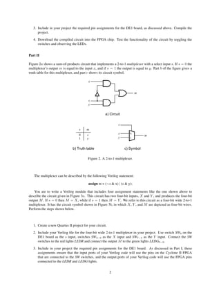
2. Designing a 4-bit 2-to-1 multiplexer circuit to select between two 4-bit inputs based on a selection bit.
3. Building a 2-bit wide 3-to-1 multiplexer using two 2-to-1 multiplexers to select between three 2-bit inputs.
The circuits are tested by toggling switches and observing the output LEDs. This allows learning how to interface
inputs and outputs to an FPGA and implement basic multiplexer logic.
![Laboratory Exercise 1
Switches, Lights, and Multiplexers
The purpose of this exercise is to learn how to connect simple input and output devices to an FPGA chip and
implement a circuit that uses these devices. We will use the switches SW9−0 on the DE1 board as inputs to the
circuit. We will use light emitting diodes (LEDs) and 7-segment displays as output devices.
Part I
The DE1 board provides 10 toggle switches, called SW9−0 , that can be used as inputs to a circuit, and 10 red
lights, called LEDR9−0 , that can be used to display output values. Figure 1 shows a simple Verilog module that
uses these switches and shows their states on the LEDs. Since there are 10 switches and lights it is convenient to
represent them as vectors in the Verilog code, as shown. We have used a single assignment statement for all 10
LEDR outputs, which is equivalent to the individual assignments
assign LEDR[9] = SW[9];
assign LEDR[8] = SW[8];
...
assign LEDR[0] = SW[0];
The DE1 board has hardwired connections between its FPGA chip and the switches and lights. To use SW9−0 and
LEDR9−0 it is necessary to include in your Quartus II project the correct pin assignments, which are given in the
DE1 User Manual. For example, the manual specifies that SW0 is connected to the FPGA pin L22 and LEDR0 is
connected to pin R20. A good way to make the required pin assignments is to import into the Quartus II software
the file called DE1_pin_assignments.qsf, which is provided on the DE1 System CD and in the University Program
section of Altera’s web site. The procedure for making pin assignments is described in the tutorial Quartus II
Introduction using Verilog Design, which is also available from Altera.
It is important to realize that the pin assignments in the DE1_pin_assignments.qsf file are useful only if the
pin names given in the file are exactly the same as the port names used in your Verilog module. The file uses the
names SW[0] . . . SW[9] and LEDR[0] . . . LEDR[9] for the switches and lights, which is the reason we used these
names in Figure 1.
// Simple module that connects the SW switches to the LEDR lights
module part1 (SW, LEDR);
input [9:0] SW; // toggle switches
output [9:0] LEDR; // red LEDs
assign LEDR = SW;
endmodule
Figure 1. Verilog code that uses the DE1 board switches and lights.
Perform the following steps to implement a circuit corresponding to the code in Figure 1 on the DE1 board.
1. Create a new Quartus II project for your circuit. Select Cyclone II EP2C20F484C7 as the target chip, which
is the FPGA chip on the Altera DE1 board.
2. Create a Verilog module for the code in Figure 1 and include it in your project.
1](https://image.slidesharecdn.com/lab1verilog-130207211842-phpapp01/85/Lab1-verilog-1-320.jpg)


![c1 c0 Character
00 d
01 E
10 1
11
Table 1. Character codes.
Perform the following steps:
1. Create a new Quartus II project for your circuit.
2. Create a Verilog module for the 7-segment decoder. Connect the c1 c0 inputs to switches SW1−0 , and connect
the outputs of the decoder to the HEX0 display on the DE1 board. The segments in this display are called
HEX00 , HEX01 , . . ., HEX06 , corresponding to Figure 6. You should declare the 7-bit port
output [0:6] HEX0;
in your Verilog code so that the names of these outputs match the corresponding names in the DE1 User
Manual and the DE1_pin_assignments.qsf file.
3. After making the required DE1 board pin assignments, compile the project.
4. Download the compiled circuit into the FPGA chip. Test the functionality of the circuit by toggling the
SW1−0 switches and observing the 7-segment display.
Part V
Consider the circuit shown in Figure 7. It uses a two-bit wide 3-to-1 multiplexer to enable the selection of three
characters that are displayed on a 7-segment display. Using the 7-segment decoder from Part IV this circuit can
display any of the characters D, E, 1, and ‘blank’. The character codes are set according to Table 1 by using the
switches SW5−0 , and a specific character is selected for display by setting the switches SW9−8 .
An outline of the Verilog code that represents this circuit is provided in Figure 8. Note that we have used the
circuits from Parts III and IV as subcircuits in this code. You are to extend the code in Figure 8 so that it uses
three 7-segment displays rather than just one. You will need to use three instances of each of the subcircuits. The
purpose of your circuit is to display any word on the four displays that is composed of the characters in Table 1,
and be able to rotate this word in a circular fashion across the displays when the switches SW9−8 are toggled. As
an example, if the displayed word is dE1, then your circuit should produce the output patterns illustrated in Table
2.
SW 9
SW 8
2 0
SW 5 – 4
2 00 5 1
2
SW 3 – 2 01 7-segment 7 6
10
SW 1 – 0 2 decoder
4 2
3
Figure 7. A circuit that can select and display one of three characters.
6](https://image.slidesharecdn.com/lab1verilog-130207211842-phpapp01/85/Lab1-verilog-6-320.jpg)
![module part5 (SW, HEX0);
input [9:0] SW; // toggle switches
output [0:6] HEX0; // 7-seg displays
wire [1:0] M;
mux_2bit_3to1 M0 (SW[9:8], SW[5:4], SW[3:2], SW[1:0], M);
char_7seg H0 (M, HEX0);
endmodule
// implements a 2-bit wide 3-to-1 multiplexer
module mux_2bit_3to1 (S, U, V, W, M);
input [1:0] S, U, V, W;
output [1:0] M;
. . . code not shown
endmodule
// implements a 7-segment decoder for d, E, 1 and ‘blank’
module char_7seg (C, Display);
input [1:0] C; // input code
output [0:6] Display; // output 7-seg code
. . . code not shown
endmodule
Figure 8. Verilog code for the circuit in Figure 7.
SW9 SW8 Character pattern
00 d E 1
01 E 1 d
10 1 d E
Table 2. Rotating the word dE1 on three displays.
Perform the following steps.
1. Create a new Quartus II project for your circuit.
2. Include your Verilog module in the Quartus II project. Connect the switches SW9−8 to the select inputs of
each of the three instances of the three-bit wide 3-to-1 multiplexers. Also connect SW5−0 to each instance
of the multiplexers as required to produce the patterns of characters shown in Table 2. Connect the outputs
of the three multiplexers to the 7-segment displays HEX2, HEX1, and HEX0.
3. Include the required pin assignments for the DE1 board for all switches, LEDs, and 7-segment displays.
Compile the project.
7](https://image.slidesharecdn.com/lab1verilog-130207211842-phpapp01/85/Lab1-verilog-7-320.jpg)


![– Como conceber transformações? [Setor Privado]](https://cdn.slidesharecdn.com/ss_thumbnails/cafcombpmsetorprivadocomoconcebertransformaes-150321135043-conversion-gate01-160122141409-thumbnail.jpg?width=640&height=640&fit=bounds)