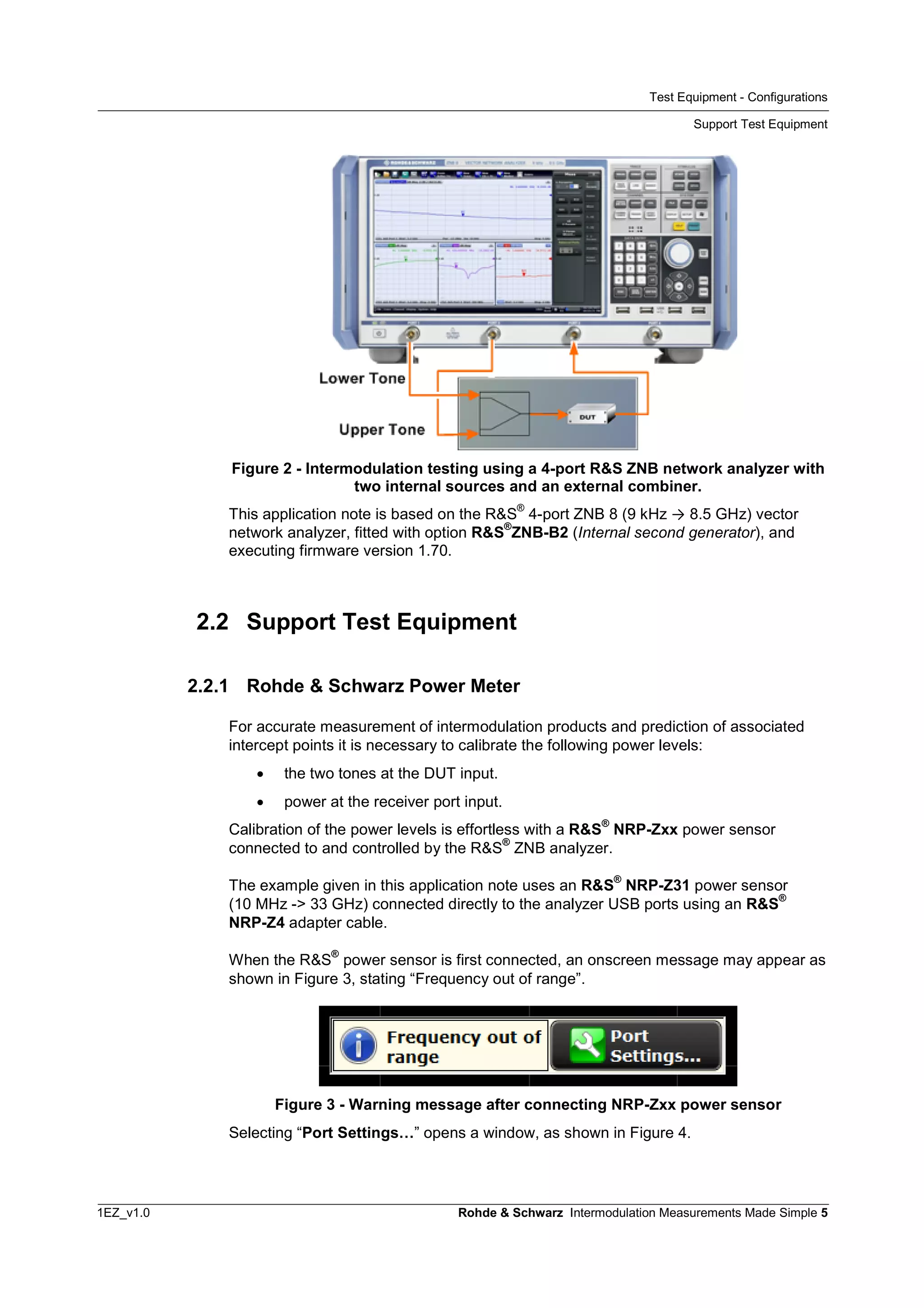
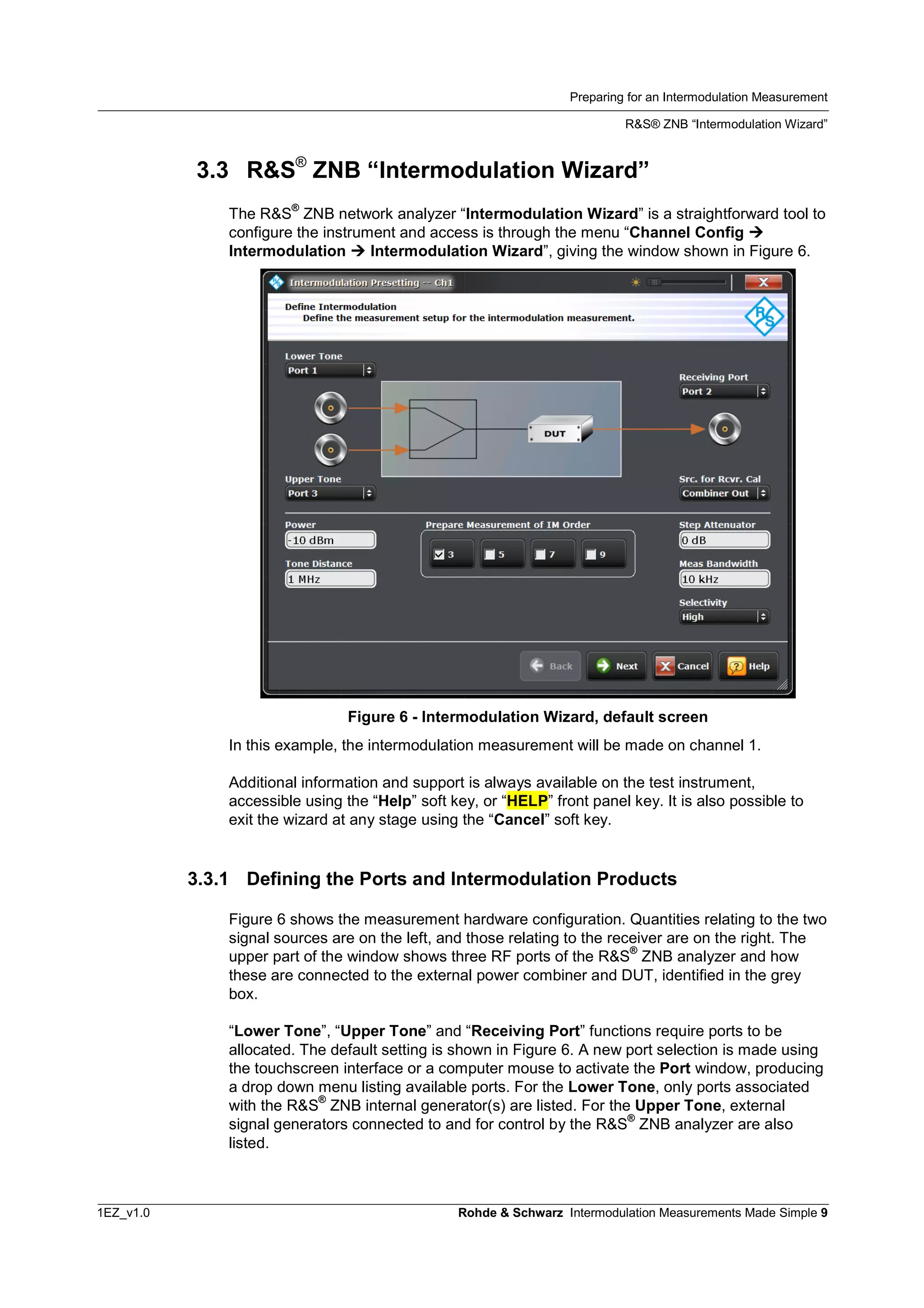
The "Intermodulation Wizard" tool in the R&S ZNB vector network analyzer quickly configures the instrument for intermodulation measurements. It defines the signal sources, receiver port, measurement bandwidth, and intermodulation product orders to measure. The wizard guides the user through setting the signal frequencies and powers, and calibrating the power levels before making swept or CW intermodulation measurements.
Measuring the cutoff frequency of a low pass filterHasnain Ali
It is required to setup an automated test and measurement system for measuring the cutoff frequency of a low pass filter using LabView and estimate the frequency response of the filter.
Measuring the cutoff frequency of a low pass filterHasnain Ali
It is required to setup an automated test and measurement system for measuring the cutoff frequency of a low pass filter using LabView and estimate the frequency response of the filter.
digital down-converter (DDC) converts a digitized real signal centered at an intermediate frequency (IF) to a basebanded complex signal centered at zero frequency. In addition to downconversion
USB 3.1 Gen 2 Compliance Testing and Debug Webinarteledynelecroy
Join Teledyne LeCroy for this free webinar as we analyze the major changes in the standard compared to its previous versions and offer solutions for compliance testing and debug to help in analysis and characterization of USB 3.1 Gen 2 signals and interfaces.
CMOS Analog IC design by Dr GS Javed - Refresher Course - Batch 1Javed G S, PhD
Topics covered in the course
1. DC Biasing of the circuits
2. Circuits for reference voltage and current generation
-Voltage Regulator
-BGR
-LDO
-V-to-I
3. Precision Current References
4. Opamp design for Analog to digital converters
- OTA
- Buffer
- Unity Feedback OTA
- Layout design strategies – 2stage opamp + CMFB
5. Sense and Return mechanisms in Feedback circuits
- Current and Voltage circuits
6. Sub-Threshold Conduction
- Low voltage Operation
7. ADC Design and Simulation
-Near Nyquist performance of Opamp for ADC Circuits
-Spectral Analysis and No. of FFT Points for simulation
-Simulation time for performance
-Resistors – their variation and Calibration
-Switch design for S/H
-CDAC
8. On-Chip Inductors
Liquid Sensing: Visible light absorption spectroscopy and colorimetry are two fundamental tools used in chemical analysis. Most of these light-based systems use photodiodes as the light sensor, and require similar high input impedance signal chains. This session examines the different components of a photodiode amplifier signal chain, including a programmable gain transimpedance amplifier, a hardware lock-in amplifier, and a Σ-Δ ADC that can measure a sample and reference channel to greatly reduce any measurement error due to variations in intensity of the light source.
Gas Sensing: Many industrial processes involve toxic compounds, and it is important to know when dangerous concentrations exist. Electrochemical sensors offer several advantages for instruments that detect or measure the concentration of toxic gases. This session will describe a portable toxic gas detector using an electrochemical sensor. The system presented here includes a potentiostat circuit to drive the sensor, as well as a transimpedance amplifier to take the very small output current from the sensor and translate it to a voltage that can take advantage of the full-scale input of an ADC.
The USB 2.0 standard is widely deployed in both computer and embedded systems. Compliance testing for this standard includes signal integrity as well as a number of low-level protocol tests.
This presentation provides an overview of the test requirements for USB 2.0 compliance and provide background on each test case. Details of fixtures and signal integrity requirements are highlighted in detail.
For more information visit http://rohde-schwarz-scopes.com or call (888) 837-8772 to speak to a local Rohde & Schwarz expert.
Join us for a LIVE WEBINAR on this topic! Wednesday, November 14, 2:00pm ET
http://bit.ly/XPgjO7
Wide bandwidth modulation is becoming more common in communications. The emergence of the 802.11ac wireless Ethernet standard has extended the modulation bandwidth to 160 MHz which requires very wide band measurement equipment to measure. This presentation illustrates the details of a measurement method that uses a real time digital down converter and post processing software that measures the performance of this signal.
Analog-to-Digital Converter (ADC) is an integral part of high-speed signal processing applications. This paper discusses about 10-bit SAR based ADC that enables very low power consumption and sampling rate as high as 165 MSPS.
(Slides from Live webinar on September 25, 2014, presented by Mike Schnecker. Watch the webinar On-Demand here: http://goo.gl/LkjUUg)
Attendees Will Learn:
An overview of switched mode power supplies
Common measurements (ie, what to measure and why)
Circuit loading and probing considerations
How instrument specifications impact measurement accuracy
Switched mode power supplies have become ubiquitous in electronics as they provide precise voltages including high power with very high efficiency. The efficiency of these power supplies requires low loss power transistors and the design requires measurement of highly dynamic voltages. Voltage levels can vary from millivolts to hundreds of volts in some applications.
In this webinar, the proper use of a digital oscilloscope to accurately measure these voltages will be discussed along with key aspects of instrument performance such as noise and overdrive recovery that affect the accuracy of the measurement.
Basic blocks to understand RFFE Architecture. how Analog front end and Digital front is different. Basic components like Filter, Mixer, Power Amplifier, circulator, Duplexer, LNA and demodulator working is explained. It can held to design your own front end as RF link budget has been explained in well manner. what to do to avoid saturation of PA?
Frequency Synthesis and Clock Generation for High Speed Systems - VE2013Analog Devices, Inc.
Frequency synthesis and clock generation are now key elements in all aspects of high speed data acquisition and RF design. In this session, the primary types of frequency synthesizers—phase-locked loops (PLL) and direct digital synthesizers (DDS)—are discussed, along with the applications for when each is appropriate. Also covered are detailed aspects of synthesizer design. Other applications, such as clock distribution and translation are addressed, and problems associated with poor clocking are identified. Examples of poor clocking are shown, along with the results of doing it properly.
Why to do single-tone desense test ?
What is cross modulation ?
what's the difference between cross modulation and intermodulation ?
what is triple beat ?
Sensitivity or selectivity - How does eLNA impact the receriver performancecriterion123
it describes
1. Why need external LNA ?
2. Why does poor linearity lead to poor sensitivity ?
3. For the eLNA gain, the more the better ?
4. Why can SAW filter improve linearity ?
PA Intermodulation Distortion Measurements Using the PNA ls234
Presentation by Maria Jesus Canavate Sanchez, 'PA Intermodulation Distortion Measurements Using the PNA', on Wednesday 16 December at Heriot-Watt University
LTE Measurement: How to test a device
This course provides an overview with practical examples and exercises on how to test a LTE-capable device while performing standardized RF measurements such as power, signal quality, spectrum and receier sensitivity, and how to automate these measurements in a simple and cost-effective way. We will present testing of LTE handsets in terms of protocol signaling scenarios and handover to other radio technologies for interoperability. This course will demonstrate end-to-end (E2E), throughput and application testing using the Rohde & Schwarz R&S®CMW500 Wideband Radio Communication Tester. Examles of application tests are voice over LTE, (VoLTE) or Video over LTE.
The aim of this list of programming languages is to include all notable programming languages in existence, both those in current use and ... Note: This page does not list esoteric programming languages. .... Computer programming portal ...
1. R&S® ZNB Vector Network
Analyzer – Intermodulation
Measurements Made Simple.
Application Note
Products:
| ZNBx vector network
analyzer
The family of ZNB vector network
analyzers from Rohde & Schwarz has
several features to provide effective
characterization of intermodulation
products of non-linear RF devices.
The “Intermodulation Wizard” quickly
configures the instrument for use,
including power calibration and formatted
results. The extensive power range
enables accurate and simultaneous
measurement of up to four odd product
orders, and presentation of the related
intercept points.
Concurrent measurements of fixed and
swept frequencies are further reduced in
time with the optional second internal
frequency source.
This Application Note provides guidance
on using the “Intermodulation Wizard”
through an example measurement.
IntermodulationMeasurements
madesimple
MarkBailey
2013-03-27,1EZ63,Version1.0
2. Table of Contents
1EZ_v1.0 Rohde & Schwarz Intermodulation Measurements Made Simple 2
Table of Contents
1 Introduction ............................................................................ 3
2 Test Equipment - Configurations.......................................... 3
2.1 R&S
®
ZNB Vector Network Analyzer ..........................................................4
2.2 Support Test Equipment..............................................................................5
2.2.1 Rohde & Schwarz Power Meter...................................................................5
2.2.2 Power Combiner...........................................................................................6
2.3 Device Under Test (DUT) .............................................................................7
3 Preparing for an Intermodulation Measurement ................. 7
3.1 Presetting the R&S
®
ZNB Vector Network Analyzer.................................7
3.2 Defining the Measurement Requirements .................................................8
3.3 R&S
®
ZNB “Intermodulation Wizard”.........................................................9
3.3.1 Defining the Ports and Intermodulation Products....................................9
3.3.2 Frequencies and Powers...........................................................................10
3.3.3 Measurement Parameters..........................................................................12
3.3.4 Completing the Intermodulation Wizard ..................................................13
3.4 Intermodulation Power Flatness Calibration...........................................14
3.4.1 Power Meter Settings.................................................................................16
4 Making an Intermodulation Measurement.......................... 17
4.1 Swept Frequency Measurement ...............................................................17
4.1.1 Trace Label Descriptions...........................................................................18
4.1.2 Editing Measurement Traces ....................................................................19
4.2 Continuous Wave (CW) Measurement .....................................................20
5 Editing the Intermodulation Measurement Configuration. 22
6 Bibliography ......................................................................... 23
7 Additional Information......................................................... 23
3. Introduction
R&S® ZNB Vector Network Analyzer
1EZ_v1.0 Rohde & Schwarz Intermodulation Measurements Made Simple 3
1 Introduction
Measuring intermodulation products (IMP) of a non-linear RF device typically involves
three pieces of test equipment, and time to connect and calibrate multiple cable path
losses. Once the equipment is configured, the measurement is straightforward for a
simple fixed frequency two tone measurement. However, preparing for a swept
frequency response is more complex, requiring synchronization of frequency sources.
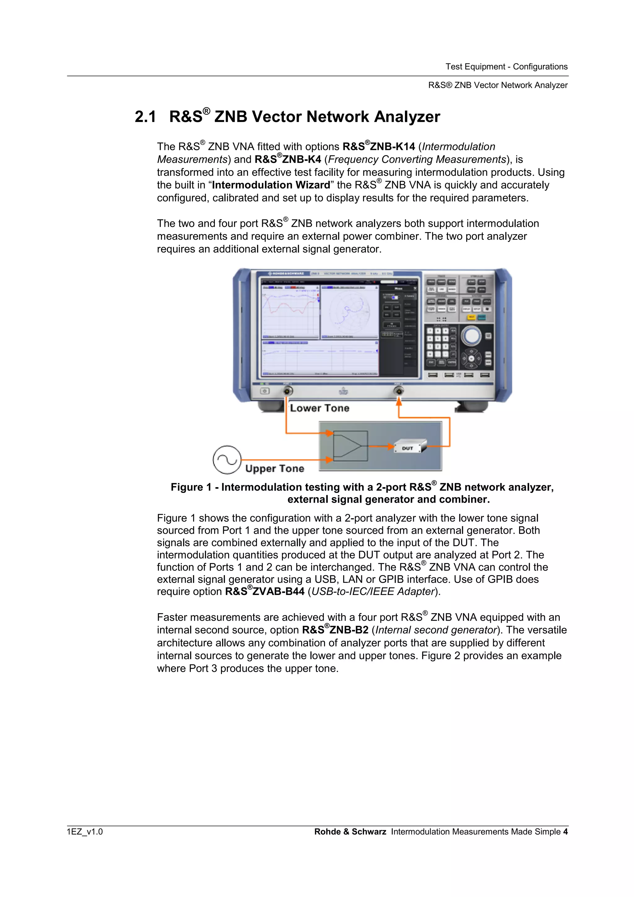
The R&S
®
ZNB vector network analyzer (VNA) is a versatile self-contained instrument
able to measure intermodulation products accurately and effortlessly provides the
following benefits:
‘Intermodulation Wizard’ tool to efficiently configure the instrument.
Faster measurements with an internal second source.
Generous linear source output power.
Excellent receiver sensitivity for detecting low level higher order products.
Excellent receiver linearity (Absolute max input, +27 dBm).
Simultaneous measurement of fixed and swept frequencies.
Straightforward power calibration.
Formatted results.
Display of calculated odd order intercept points (3
rd
, 5
th
, 7
th
and 9
th
).
In this application note, step-wise instructions are presented on how to set up the
R&S
®
ZNB VNA, leading to the successful measurement of intermodulation products.
This compliments the information given in the R&S ZNB, Vector Network Analyzers,
User Manual,
[1]
and the on-instrument “HELP”.
It is assumed that the reader is familiar with the theory and limitations caused by the
generation of intermodulation products in non-linear RF devices. Detailed information
is given in chapter 2 of R&S
®
Application Note, Intermodulation Distortion
Measurements on Modern Spectrum Analyzers, (1EF79),
[2]
available on the Rohde &
Schwarz website.
2 Test Equipment - Configurations
The measurement of intermodulation products involves the application of two RF
sources of equal power and close in frequency, that are combined into a single path
applied to a device under test (DUT). The RF output spectrum from the DUT is
analyzed for the presence of spurious frequencies caused by the non-linear behaviour
of the DUT. The source input power levels may need to be varied to observe the
intermodulation products. Once measured, this information is used to calculate the
intermodulation product intercept point, either referred to the DUT input or output.
4. Test Equipment - Configurations
R&S® ZNB Vector Network Analyzer
1EZ_v1.0 Rohde & Schwarz Intermodulation Measurements Made Simple 4
2.1 R&S®
ZNB Vector Network Analyzer
The R&S
®
ZNB VNA fitted with options R&S
®
ZNB-K14 (Intermodulation
Measurements) and R&S
®
ZNB-K4 (Frequency Converting Measurements), is
transformed into an effective test facility for measuring intermodulation products. Using
the built in “Intermodulation Wizard” the R&S
®
ZNB VNA is quickly and accurately
configured, calibrated and set up to display results for the required parameters.
The two and four port R&S
®
ZNB network analyzers both support intermodulation
measurements and require an external power combiner. The two port analyzer
requires an additional external signal generator.
Figure 1 - Intermodulation testing with a 2-port R&S
®
ZNB network analyzer,
external signal generator and combiner.
Figure 1 shows the configuration with a 2-port analyzer with the lower tone signal
sourced from Port 1 and the upper tone sourced from an external generator. Both
signals are combined externally and applied to the input of the DUT. The
intermodulation quantities produced at the DUT output are analyzed at Port 2. The
function of Ports 1 and 2 can be interchanged. The R&S
®
ZNB VNA can control the
external signal generator using a USB, LAN or GPIB interface. Use of GPIB does
require option R&S
®
ZVAB-B44 (USB-to-IEC/IEEE Adapter).
Faster measurements are achieved with a four port R&S
®
ZNB VNA equipped with an
internal second source, option R&S
®
ZNB-B2 (Internal second generator). The versatile
architecture allows any combination of analyzer ports that are supplied by different
internal sources to generate the lower and upper tones. Figure 2 provides an example
where Port 3 produces the upper tone.
5. Test Equipment - Configurations
Support Test Equipment
1EZ_v1.0 Rohde & Schwarz Intermodulation Measurements Made Simple 5
Figure 2 - Intermodulation testing using a 4-port R&S ZNB network analyzer with
two internal sources and an external combiner.
This application note is based on the R&S
®
4-port ZNB 8 (9 kHz ® 8.5 GHz) vector
network analyzer, fitted with option R&S
®
ZNB-B2 (Internal second generator), and
executing firmware version 1.70.
2.2 Support Test Equipment
2.2.1 Rohde & Schwarz Power Meter
For accurate measurement of intermodulation products and prediction of associated
intercept points it is necessary to calibrate the following power levels:
the two tones at the DUT input.
power at the receiver port input.
Calibration of the power levels is effortless with a R&S
®
NRP-Zxx power sensor
connected to and controlled by the R&S
®
ZNB analyzer.
The example given in this application note uses an R&S
®
NRP-Z31 power sensor
(10 MHz -> 33 GHz) connected directly to the analyzer USB ports using an R&S
®
NRP-Z4 adapter cable.
When the R&S
®
power sensor is first connected, an onscreen message may appear as
shown in Figure 3, stating “Frequency out of range”.
Figure 3 - Warning message after connecting NRP-Zxx power sensor
Selecting “Port Settings…” opens a window, as shown in Figure 4.
6. Test Equipment - Configurations
Support Test Equipment
1EZ_v1.0 Rohde & Schwarz Intermodulation Measurements Made Simple 6
Figure 4 - Port Settings for Channel 1
In this example, the power meter has been correctly identified as being an R&S
®
NRP-
Z31, and has a minimum frequency response greater than the minimum frequency
response of the R&S
®
ZNB. Therefore, the user must ensure that the test configuration
is within the operating limits of the instruments.
2.2.2 Power Combiner
Measurement of intermodulation products requires two test tones to be combined into
a single RF path using a passive power combiner.
The choice of combiner should take into account:
Frequency
bandwidth
The operating bandwidth of the combiner must be
considerably greater than the spectrum of the
intermodulation products.
Coupling
factor
This should be kept to a minimum to reduce insertion loss
through the combiner.
Isolation The combiner must provide sufficient isolation between the
two sources (>6 dB).
In the following example, a resistive power combiner from Mini-Circuits (ZFRSC-
183+
[4]
) is used, giving typically 6.5 dB of coupling loss and isolation, from DC to 18
GHz.
7. Preparing for an Intermodulation Measurement
Device Under Test (DUT)
1EZ_v1.0 Rohde & Schwarz Intermodulation Measurements Made Simple 7
2.3 Device Under Test (DUT)
The RF amplifier example used in this application note is from Mini-Circuits (ZJL-
3G+
[3]
). This has the following typical characteristics:
Frequency range: 20 MHz ® 3 GHz
Gain: 19 dB
Output 1 dB compression point: +8 dBm
Output 3
rd
order intercept point: +22 dBm
3 Preparing for an Intermodulation
Measurement
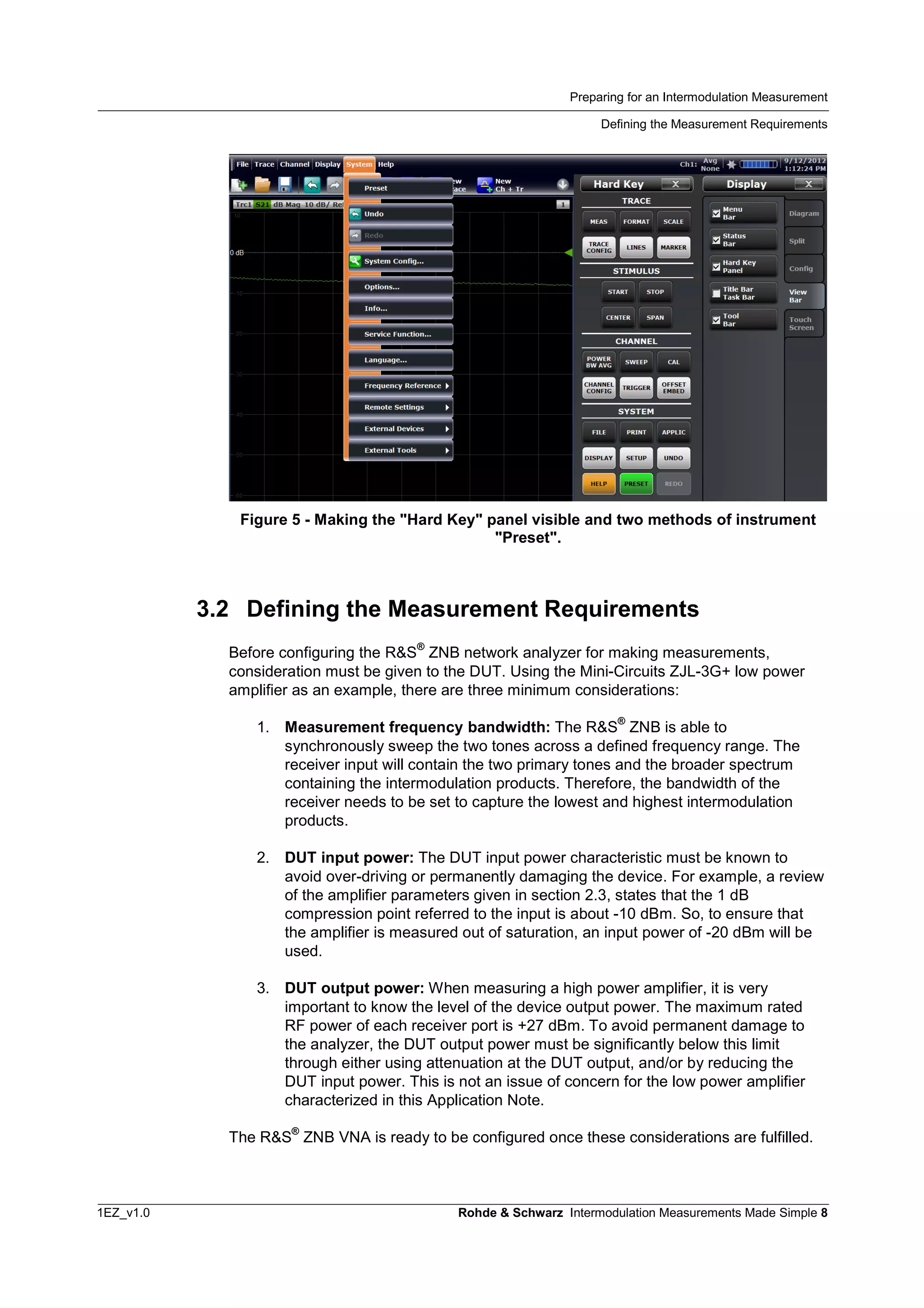
3.1 Presetting the R&S®
ZNB Vector Network Analyzer
Presetting the R&S
®
ZNB network analyzer to its factory default settings will avoid the
unexpected effects of any legacy settings. Refer to the R&S ZNB, Vector Network
Analyzers, User Manual, or press the “HELP” button on the instrument front panel
keypad for more information on preset conditions.
Selection of any function on the R&S
®
ZNB VNA is designed to be simple and is
possible in at least two ways. Using “Preset” as an example:
1. Front panel keypad: “SYSTEM” key group > “PRESET”.
2. Software menu structure: “SYSTEM Preset”.
3. Software based hard key panel: “PRESET”.
The hard key panel is hidden by default, but is useful when operating the instrument
remotely. The hard key panel can be displayed using “DISPLAY View Bar Hard
Key Panel”, as shown in Figure 5.
8. Preparing for an Intermodulation Measurement
Defining the Measurement Requirements
1EZ_v1.0 Rohde & Schwarz Intermodulation Measurements Made Simple 8
Figure 5 - Making the "Hard Key" panel visible and two methods of instrument
"Preset".
3.2 Defining the Measurement Requirements
Before configuring the R&S
®
ZNB network analyzer for making measurements,
consideration must be given to the DUT. Using the Mini-Circuits ZJL-3G+ low power
amplifier as an example, there are three minimum considerations:
1. Measurement frequency bandwidth: The R&S
®
ZNB is able to
synchronously sweep the two tones across a defined frequency range. The
receiver input will contain the two primary tones and the broader spectrum
containing the intermodulation products. Therefore, the bandwidth of the
receiver needs to be set to capture the lowest and highest intermodulation
products.
2. DUT input power: The DUT input power characteristic must be known to
avoid over-driving or permanently damaging the device. For example, a review
of the amplifier parameters given in section 2.3, states that the 1 dB
compression point referred to the input is about -10 dBm. So, to ensure that
the amplifier is measured out of saturation, an input power of -20 dBm will be
used.
3. DUT output power: When measuring a high power amplifier, it is very
important to know the level of the device output power. The maximum rated
RF power of each receiver port is +27 dBm. To avoid permanent damage to
the analyzer, the DUT output power must be significantly below this limit
through either using attenuation at the DUT output, and/or by reducing the
DUT input power. This is not an issue of concern for the low power amplifier
characterized in this Application Note.
The R&S
®
ZNB VNA is ready to be configured once these considerations are fulfilled.
9. Preparing for an Intermodulation Measurement
R&S® ZNB “Intermodulation Wizard”
1EZ_v1.0 Rohde & Schwarz Intermodulation Measurements Made Simple 9
3.3 R&S®
ZNB “Intermodulation Wizard”
The R&S
®
ZNB network analyzer “Intermodulation Wizard” is a straightforward tool to
configure the instrument and access is through the menu “Channel Config
Intermodulation Intermodulation Wizard”, giving the window shown in Figure 6.
Figure 6 - Intermodulation Wizard, default screen
In this example, the intermodulation measurement will be made on channel 1.
Additional information and support is always available on the test instrument,
accessible using the “Help” soft key, or “HELP” front panel key. It is also possible to
exit the wizard at any stage using the “Cancel” soft key.
3.3.1 Defining the Ports and Intermodulation Products
Figure 6 shows the measurement hardware configuration. Quantities relating to the two
signal sources are on the left, and those relating to the receiver are on the right. The
upper part of the window shows three RF ports of the R&S
®
ZNB analyzer and how
these are connected to the external power combiner and DUT, identified in the grey
box.
“Lower Tone”, “Upper Tone” and “Receiving Port” functions require ports to be
allocated. The default setting is shown in Figure 6. A new port selection is made using
the touchscreen interface or a computer mouse to activate the Port window, producing
a drop down menu listing available ports. For the Lower Tone, only ports associated
with the R&S
®
ZNB internal generator(s) are listed. For the Upper Tone, external
signal generators connected to and for control by the R&S
®
ZNB analyzer are also
listed.
10. Preparing for an Intermodulation Measurement
R&S® ZNB “Intermodulation Wizard”
1EZ_v1.0 Rohde & Schwarz Intermodulation Measurements Made Simple 10
Selection of unsupported port combinations will result in an
error message which automatically clears when the test
conditions are corrected.
“Src. for Rcvr. Cal” selects the signal source used for
calibrating the power level at the receiver port. Figure 7 shows
the available power sources from the drop down menu. By
default, the output from the combiner and Port 4 of the
analyzer are offered as power sources. Figure 7 also shows a
R&S
®
SGS 100A signal generator connected to the analyzer,
“Gen 1”. For this example “Combiner Out” is used.
The bottom part of Figure 6 configures the source and receiver parameters. Values are
input for source Power, Tone Distance and the receiver filter Measurement
Bandwidth. The Measurement Bandwidth and Tone Distance values need to be
chosen with care. The Tone Distance should be greater than 100x the Measurement
Bandwidth, so that each frequency component is selected by the filter without
interference. The analyzer will present an information window if this condition is not
fulfilled.
“Prepare Measurement of IM Order” allows the intermodulation product orders of
interest to be selected by placing a ‘tick’ in the appropriate boxes. This information
allows the R&S
®
ZNB VNA to optimize its configuration, avoiding measurement of
unnecessary data. Hence the wanted measurements are collected more quickly.
“Step Attenuator“ refers to analyzers fitted with option R&S
®
ZNB-B3x (Receiver Step
Attenuator) to allow measurement of higher input power levels.
“Selectivity” of the IF filter can be changed and by default is set to “High”, to maximize
rejection of adjacent spurious frequency components.
Example (Amplifier ZJL-3G+): All parameters are default except:
Source Power level = -20 dBm
All intermodulation orders are selected.
Once configured, press “Next”. It is possible to come back to this window and change
these parameters at any time.
3.3.2 Frequencies and Powers
Stage two of the Intermodulation Wizard defines the start and stop frequencies, and
output power of the sources. If the start and stop frequencies exceed the hardware
capabilities of the instrument, then a warning message will appear and the frequency
range text will be highlighted in red for the port(s) attempting to operate beyond
hardware limits, as shown in Figure 8.
Figure 7 – Receiver
calibration: Power
source options
11. Preparing for an Intermodulation Measurement
R&S® ZNB “Intermodulation Wizard”
1EZ_v1.0 Rohde & Schwarz Intermodulation Measurements Made Simple 11
Figure 8 - Frequency range: Defining and viewing exceeded limits
The “Start Frequency” and “Stop Frequency” values are referenced to the port
sourcing the lower tone. This port is used to set the frequency ranges for the other
ports. In this example, Port 1 sources the lower tone and Port 3 the upper tone, offset
by 1 MHz. Therefore the hardware upper limit of Port 3 is exceeded by 1 MHz,
requiring that the “Stop Frequency” of Port 1 must be reduced by at least 1 MHz.
For the receiver (Port 2), Figure 8 shows that the hardware limits for the lower and
upper frequency ranges are exceeded. When the two source tones are set to the
minimum frequency, the calculated lower 9
th
order intermodulation product is below the
measured frequency range. Similarly, when the tones are set to the maximum
frequency limit, the higher 9
th
order intermodulation product is above the measured
frequency range.
Therefore the measurement frequency range must be configured so that all of the VNA
ports and the power meter are within their operating frequency ranges. For the
analyzer only, this can be done automatically using the “Fit Frequency Range” soft
key. When using this method, take care to ensure that the power meter frequency
range matches or exceeds the required test measurement frequency range.
Example (Amplifier ZJL-3G+): The lower tone frequency range and
power level are set as follows, and implemented as shown in Figure 9:
Start frequency = 15 MHz
Stop frequency = 3.5 GHz
Power = -20 dBm
The 10 MHz low frequency limit of the R&S NRP31 power sensor defines the Start
Frequency. At 15 MHz the lowest 9
th
order product is safely measured at 11 MHz. The
Stop Frequency is 3.5 GHz, since the amplifier is not specified beyond 3 GHz.
12. Preparing for an Intermodulation Measurement
R&S® ZNB “Intermodulation Wizard”
1EZ_v1.0 Rohde & Schwarz Intermodulation Measurements Made Simple 12
Figure 9 – Setting the reference frequency range and power level
Once configured, press “Next”. It is possible to come back to this window and change
these parameters at any time. Or go “Back” to the previous step if necessary.
3.3.3 Measurement Parameters
The measured parameters that will be displayed need to be chosen. The selected
items will each have a trace and will be shown together on one display. The available
measurement parameters are shown in Figure 10 and are selected by placing a tick in
the adjacent box: The available parameters are:
Output intermodulation products
Calculated intercept points
Input tone levels
Output tone levels
If parameters are greyed out, then the associated intermodulation product order was
not selected in step 1 of the Intermodulation Wizard, “Define Intermodulation” (see
Figure 6). It is possible to change the selected order using the “Back” button to return
to step 1 of the wizard.
13. Preparing for an Intermodulation Measurement
R&S® ZNB “Intermodulation Wizard”
1EZ_v1.0 Rohde & Schwarz Intermodulation Measurements Made Simple 13
Figure 10 – Selection of available measurement parameters
Intermodulation Products – These are all referenced to the DUT output and for each
order of intermodulation product, any of the following can be shown:
Low side intermodulation product
High side intermodulation product
“Major Prod.” – Derived from the greater of the upper and lower products at
each measured frequency point.
Intercept Point - Calculated from the “Major Prod.” result for each order.
Tone Power Level – Measurement of the input and output levels of the two tones are
selected at the bottom of the window.
Example (Amplifier ZJL-3G+): Figure 10 shows that the following
parameters have been selected for measurement.
3
rd
order intermodulation lower and upper products
3
rd
order intercept point
Lower and upper tone levels at the DUT input
Lower and upper tone levels at the DUT output
Once configured, press “Next”. It is possible to come back to this window and change
these parameters at any time. Or go “Back” to the previous step if necessary.
3.3.4 Completing the Intermodulation Wizard
With the measurement defined and results parameters selected, the final step in the
wizard is shown in Figure 11. This provides two options, either to perform a power level
calibration, or to finish without a calibration.
14. Preparing for an Intermodulation Measurement
Intermodulation Power Flatness Calibration
1EZ_v1.0 Rohde & Schwarz Intermodulation Measurements Made Simple 14
Figure 11 – Completing the Intermodulation Wizard
This is a good opportunity to review the measurement configuration. If changes are
needed, use the “Back” soft key to reverse through the set up menus.
Select the calibration requirement and press “Finish” to complete the Intermodulation
Wizard. Regardless of the calibration state, the R&S
®
ZNB VNA will close the Wizard
and open a display with the frequency response of the parameters that were selected
in step 3 of the Intermodulation Wizard, “Measurement Parameters”.
3.4 Intermodulation Power Flatness Calibration
Coupling a R&S
®
NRP-Zxx power sensor to the R&S
®
ZNB VNA, allows the use of an
inbuilt calibration tool, “Intermodulation Power Calibration”. This ensures that the
source power levels at the input of the DUT and the measurement of the
intermodulation products at the Receiving Port are accurate across the frequency
range.
There are two ways of starting the power flatness calibration tool, either at the end of
the Intermodulation Wizard, or if in the measurement mode, through the menu:
“Channel Channel Config Intermodulation Start Power Cal…/Intermod.
Pwr. Cal…”.
15. Preparing for an Intermodulation Measurement
Intermodulation Power Flatness Calibration
1EZ_v1.0 Rohde & Schwarz Intermodulation Measurements Made Simple 15
Figure 12 – Power calibration window
Figure 12 shows the power calibration window, with the sources on the left and the
receiver port on the right. The calibration is performed in three steps:
1. With the power meter connected to the calibration plane (normally the
combiner output), press “Start Cal Sweep”, and the power response of the
Lower Tone will be characterized over frequency. The Upper Tone is off.
2. Once the Lower Tone is completed, characterization of the Upper Tone
proceeds automatically.
3. With the two sources calibrated, the port allocated to the Lower Tone is then
automatically configured to provide a reference tone at the receiver frequency
range for calibration of the Receiving Port, as shown in Figure 13. The user is
prompted to connect the combiner output to the Receiving Port and then
press “Start Cal Sweep”.
Figure 13 - Power calibration of the receiving port using the lower tone
In the first window of the Intermodulation Wizard
(Figure 6), the user selects the source for
calibrating the power flatness of the Receiving
Port. If a free analyzer port or a signal generator
is selected, this will be presented in the calibration
window as shown in Figure 14. This introduces an
extra step to the power flatness calibration,
necessitating connection of the power meter to
the source for calibration, before connecting the
source to the Receiving Port.
It is possible to step back and forth through the
steps of the power flatness calibration using the
“Prev” and “Next” soft keys.
Figure 14 – Receiver port
calibration with (left) signal
generator, (right) analyzer port 4
16. Preparing for an Intermodulation Measurement
Intermodulation Power Flatness Calibration
1EZ_v1.0 Rohde & Schwarz Intermodulation Measurements Made Simple 16
Once calibration is complete, the “Next” soft key is replaced by an “Apply” soft key,
which will apply the calibration.
3.4.1 Power Meter Settings
When starting the intermodulation power flatness calibration, in
addition to presenting the calibration tool (Figure 12), the “Pwr
Cal Settings” menu is automatically displayed (Figure 15). This
menu allows connected power meters to be configured. For the
power flatness calibration, there are three variables:
1. Max Iterations – An upper limit to the number of times that
the flatness calibration is performed, if performance within the
tolerance limit has not been achieved.
2. Tolerance – Defines a window of accepted performance,
centered on a target value. This is used during calibration and
when successfully completed, performance is checked to be
within tolerance limits.
3. Convergence – During the power flatness calibration, the
amount of power correction for each sweep is multiplied by the
convergence factor. The power correction is calculated from
the difference in measured power level at the power meter to
that at the analyzer port reference receiver. The convergence
factor is generally left set to unity.
Figure 16 presents results with the Receiving Port connected directly to the combiner
output after calibration. These responses are a measure of the R&S
®
ZNB VNA
intermodulation performance. The power level has been adjusted to 0 dBm so that the
instrument intermodulation products are above the measured noise floor. Therefore the
R&S
®
ZNB VNA has a calculated 3
rd
order intercept point greater than +30 dBm.
Figure 16 - Example of default screen after calibration
Figure 15 - Power
Sensor settings
17. Making an Intermodulation Measurement
Swept Frequency Measurement
1EZ_v1.0 Rohde & Schwarz Intermodulation Measurements Made Simple 17
4 Making an Intermodulation Measurement
4.1 Swept Frequency Measurement
Following a successful calibration, the amplifier is inserted between the combiner
output and the Receiving Port. Figure 17 shows the frequency response of the input
tones; the output tones; the output 3
rd
order intermodulation products; and the
calculated output 3
rd
order intercept point.
Figure 17 - 3rd order intermodulation characteristic of Mini-Circuits ZJL-3G+.
Input and output tone levels; intermodulation products and intercept point.
Example (Amplifier ZJL-3G+): Using the marker information in Figure
17, the performance of the amplifier at 2 GHz is summarized as:
Gain ~18.3 dB
Output 3
rd
order intermodulation products (2 GHz) ~-49 dBm
Output 3
rd
order intercept point (2 GHz) ~21.5 dBm
For the gain and 3
rd
order intercept point, this aligns with the data sheet
information (see 2.3 Device Under Test (DUT)).
NOTE: The ripple on the traces is due to the effects of impedance mismatch between
the combiner, DUT and analyzer ports. Use of attenuators reduces the effects of
mismatch at these transitions. Care must be taken not to saturate the analyzer sources
(~+12 dBm) when compensating for any additional attenuating losses before the DUT
input. Figure 18 and Figure 19 provide an example of the use of attenuators and the
improvement in performance, when compared with Figure 17 without attenuators. In
this example, 10 dB attenuators have been placed between the sources and the
combiner to provide increased isolation between the sources. The Mini-Circuits
combiner common port has a typical return loss of ~35 dB at these frequencies,
therefore providing a good input match to the DUT.
18. Making an Intermodulation Measurement
Swept Frequency Measurement
1EZ_v1.0 Rohde & Schwarz Intermodulation Measurements Made Simple 18
Other results in this application note are measured without any attenuators.
Figure 18 – Use of attenuators to reduce impedance mismatch at test interfaces
Figure 19 - 3rd order intermodulation characteristic of Mini-Circuits ZJL-3G+ with
attenuators inserted as shown in Figure 18.
4.1.1 Trace Label Descriptions
To help the User, the Intermodulation Wizard labels the result traces with suitable
acronyms. Examples are given in Table 1, and most are self-explanatory.
Label Parameter description Order
Reference
(input/output)
Unit
IM3LO Low side intermodulation product 3 Output dBm
IM5UO Upper side intermodulation product 5 Output dBm
IM7MO Major intermodulation product 7 Output dBm
LTI Lower tone Input dBm
UTO Upper Tone Output dBm
IM3MOR Major intermodulation product relative to
input tone
3 Output dBc
IP5MO Intercept Point – based on largest IMP 5 Output dBm
IP7MI Intercept Point – based on largest IMP 7 Input dBm
NLO
Noise measured at:
fnoise = flower tone - (fupper tone - flower tone) / 2
Output dBm
Table 1 - Examples of trace labels
19. Making an Intermodulation Measurement
Swept Frequency Measurement
1EZ_v1.0 Rohde & Schwarz Intermodulation Measurements Made Simple 19
4.1.2 Editing Measurement Traces
In step 1 of the Intermodulation Wizard, the intermodulation
orders for measurement are chosen. Choosing only the
wanted product orders gives a faster measurement.
In this example, 3
rd
, 5
th
, 7
th
and 9
th
orders were selected, but
are not all shown in Figure 17. However, the R&S
®
ZNB VNA
still makes the measurements for all of the selected
intermodulation products. To view the other results, either
create another trace or highlight an existing trace for change
by using the touchscreen interface. The other intermodulation
orders are accessed by entering the “Meas Intermod”
menu structure. Figure 20 shows this self-explanatory menu,
which allows single button selection of all 3
rd
order and tone
parameters.
“More IM Products…” provides access to all measured
intermodulation orders, as shown in Figure 21.
“Relative (dBc)” shows the products relative to the tone
levels.
“More Intercept…” gives access to the calculated
results for the intercept points. Figure 22 also shows
that the selected intercept point result can either be
referred to the DUT input or output.
Figure 23 shows the largest measured or “Major”
intermodulation product and intercept point for each
order. In this example, the input power of the two tones
has been increased to -15 dBm allowing the higher
order products to be measured above the noise floor.
The trace label “PCao” reflects the power level change
and shows that the power calibration is still applied.
Figure 20 – Selecting
measured parameters
Figure 21 - Selecting
Intermodulation Products
Figure 22 - Selecting
intercept points
20. Making an Intermodulation Measurement
Continuous Wave (CW) Measurement
1EZ_v1.0 Rohde & Schwarz Intermodulation Measurements Made Simple 20
Figure 23 - Amplifier measurement with 3rd, 5th, 7th and 9th intermodulation
products and intercept points.
4.2 Continuous Wave (CW) Measurement
The frequency response with two fixed frequency tones can also be displayed. This
measurement starts a new channel, which will add a trace to the existing display.
Therefore, it is best if the new channel trace is viewed on a new display (“Display
Diagram Add Trace + Diagram”). To start CW mode, access the Intermodulation
menu, “Channel Channel Config Intermodulation Add CW Mode”.
Figure 24 shows the instrument 3
rd
order intermodulation product response when the
Receiving Port is connected directly to the combiner output with the lower tone set at
1 GHz and “Max IM Order” set to 3. The IF bandwidth has been changed to 10 Hz, to
demonstrate the available dynamic range (~80 dB). Note that the source power has
changed, but the power calibration is still applied. Care should be taken when using
tone levels greater than -20 dBm at the Receiving Port since the instrument
intermodulation performance may influence the DUT results. For higher input power
levels at the Receiving Port, consider using suitable attenuation.
21. Making an Intermodulation Measurement
Continuous Wave (CW) Measurement
1EZ_v1.0 Rohde & Schwarz Intermodulation Measurements Made Simple 21
Figure 24 - CW response of the R&S
®
ZNB analyzer at 1 GHz.
The R&S
®
ZNB analyzer is optimized for sweep time and performs measurements at
discrete frequencies for the tones, products and the intermediate noise floor. The
instrument therefore automatically configures itself, selecting the appropriate Number
of Points for the intermodulation product order chosen. For example, measurement of
7
th
order IMP requires 33 points. Manually changing the Number of Points will give
erroneous results.
The amplifier intermodulation performance is shown in Figure 25.
Figure 25 – Output 3rd order intermodulation products and carrier tones
5
th
, 7
th
and 9
th
order intermodulation products can be displayed by changing the “Max
IM Order” value. Figure 26 gives an example where the input power has been
increased from -20 dBm to -15 dBm, showing intermodulation products up to and
including the 9
th
order.
22. Editing the Intermodulation Measurement Configuration.
Continuous Wave (CW) Measurement
1EZ_v1.0 Rohde & Schwarz Intermodulation Measurements Made Simple 22
Figure 26 – CW response of amplifier showing odd intermodulation products up
to 9th order
For information, the “Max IM Order” value is independent of the IMP order entered into
the Intermodulation Wizard (Figure 6).
5 Editing the Intermodulation Measurement
Configuration.
It may be necessary to change the configuration of the
intermodulation measurement and this is achieved by
returning to “Channel Config Intermodulation” (Figure
27). It is then possible to access the following options,
which return the User to the set up steps in the
Intermodulation Wizard.
“Define Intermod…” – Step 1 of the wizard, 3.3.1
Defining the Ports and
Intermodulation Products.
“Frequencies Powers…” – Step 2 of the wizard, 3.3.2
Frequencies and Powers
The other functions in the menu are used as follows:
“Reset Freq Conv Intermod” – The intermodulation
measurement mode uses
frequency conversion, i.e. the
sources and the receiver are not
on the same frequency. This soft
key returns the analyzer to normal
operation, turning off the high tone
frequency source and replacing
the intermodulation traces by a
default trace (S21). All other
settings are maintained.
Figure 27 - Editing the
intermodulation
measurement
configuration
23. Bibliography
Continuous Wave (CW) Measurement
1EZ_v1.0 Rohde & Schwarz Intermodulation Measurements Made Simple 23
“Generators…” - If an external generator source is to be used for calibrating the
receiver port, it is configured in this menu path. More details
are contained in the R&S ZNB, Vector Network Analyzers,
User Manual
[1]
, and the on-instrument “HELP” function.
“Intermod Pwr. Cal…” – Provides access to the intermodulation power calibration
routine. See section 3.4 Intermodulation Power Flatness
Calibration.
NOTE: CW mode uses a second channel. Performing a
repeat intermodulation calibration will give an invalid
response for the CW mode channel. Correct performance is
achieved through: 1) deletion of the CW mode channel; 2)
perform the intermodulation power calibration; and 3) create
a new CW mode channel.
6 Bibliography
[1] R&S ZNB, Vector Network Analyzers, User Manual, (1173.9163.02 12).
[2] R&S Intermodulation Distortion Measurements on Modern Spectrum Analyzers,
(1EF79).
[3] Mini-Circuits ZJL-3G+ Low Power Coaxial Amplifier Data Sheet.
[4] Mini-Circuits ZFRSC-183-S+ Power Splitter/ Combiner Data Sheet
7 Additional Information
This Application Note is subject to change without notice. Please visit the
website http://www.rohde-schwarz.com to download the latest versions.
Please send any comments or suggestions about this application note
to TM-Applications@rohde-schwarz.com.
24. About Rohde & Schwarz
Rohde & Schwarz is an independent group
of companies specializing in electronics. It is
a leading supplier of solutions in the fields of
test and measurement, broadcasting,
radiomonitoring and radiolocation, as well as
secure communications. Established more
than 75 years ago, Rohde & Schwarz has a
global presence and a dedicated service
network in over 70 countries. Company
headquarters are in Munich, Germany.
Environmental commitment
Energy-efficient products
Continuous improvement in
environmental sustainability
ISO 14001-certified environmental
management system
Regional contact
Europe, Africa, Middle East
+49 89 4129 12345
customersupport@rohde-schwarz.com
North America
1-888-TEST-RSA (1-888-837-8772)
customer.support@rsa.rohde-schwarz.com
Latin America
+1-410-910-7988
customersupport.la@rohde-schwarz.com
Asia/Pacific
+65 65 13 04 88
customersupport.asia@rohde-schwarz.com
This application note and the supplied
programs may only be used subject to the
conditions of use set forth in the download
area of the Rohde & Schwarz website.
R&S® is a registered trademark of Rohde & Schwarz
GmbH & Co. KG; Trade names are trademarks of the
owners.
Rohde & Schwarz GmbH & Co. KG
Mühldorfstraße 15 | D - 81671 München
Phone + 49 89 4129 - 0 | Fax + 49 89 4129 – 13777
www.rohde-schwarz.com