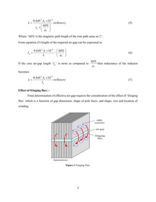
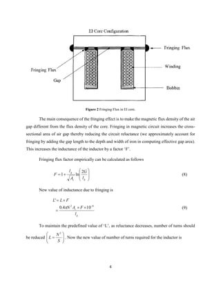
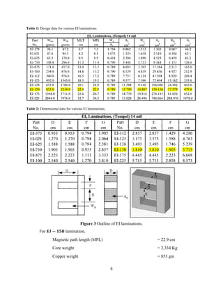
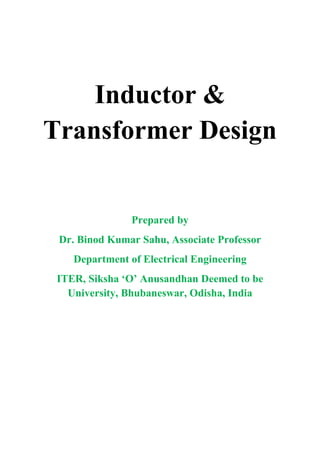
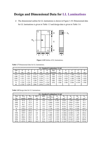
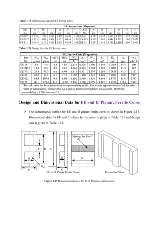
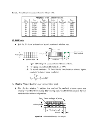
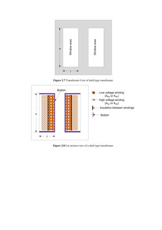
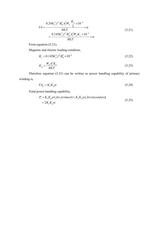
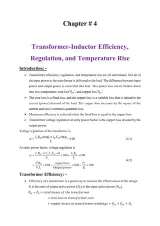
Inductor &
Transformer Design
Prepared by
Dr. Binod Kumar Sahu, Associate Professor
Department of Electrical Engineering
ITER, Siksha ‘O’ Anusandhan Deemed to be
University, Bhubaneswar, Odisha, India
Chapter # 1
Choice of Magnetic Cores
Introduction: -
 The key ingredient in a magnetic device is the magnetic field (flux) created when
current is passed through a coiled wire.
 The ability of a material to conduct magnetic flux is defined as permeability.
 A vacuum is defined as having a permeability of 1.0 and the permeability of all other
materials is measured against this baseline.
 Most materials such as air, paper, and wood are poor conductors of magnetic flux
because they have low permeability.
 There are a few materials, such as iron, nickel, cobalt, and their alloys those have high
permeabilities, sometimes ranging into the hundreds of thousands.
 These materials and their alloys are used as the base materials for all core materials.
 The main purpose of the core is to contain the magnetic flux and create a well-defined,
predictable path for the flux.
 The mean distance covered by the flux within the magnetic material, is defined as the
Magnetic Path Length (MPL). Figure 1.1 shows the magnetic path length of a magnetic
circuit.
Magnetic Path Length (MPL)
= 25+15+25+15 = 80 cm
= (Outer periphery + Inner
periphery)/2= (100+60)/2 = 80 cm
30 cm
20 cm
5 cm
5 cm
25 cm
15 cm
Figure 1.1 Magnetic path length (MPL) of a magnetic circuit.
80 cm
70 cm
10 cm
5 cm
5cm
15cm
15cm
15cm
MPL1
MPL2
Figure 1.2 Magnetic path length in shell type construction.
 What are the values of magnetic path lengths of the magnetic circuit shown in
Figure 1.2???
 The Magnetic Path Length and permeability are vital parameters for predicting the
operating characteristic of a magnetic device.
 Selection of a core material and geometry are usually based on a compromise
between conflicting requirements, such as size, weight, temperature rise, flux
density, core loss, and operating frequency.
Core Type and Shell Type Construction
 There are two types of construction for magnetic cores, core type and shell type.
 The shell type and core type constructions are shown in Figure 3.3 and Figure 3.4
respectively.
 In shell type construction core surrounds the coil.
 In the core type of construction, the coils are outside of the core. A good example of
this is a toroid, where the coil is wound on the outside of a core.
Figure 1.3 Shell type construction. Figure 1.4 Shell type construction.
Types of Core Materials
 Magnetic cores are made of three basic materials: (i) bulk metal, (ii) powdered
materials, and (iii) ferrite material.
 The bulk metals are processed from the furnace into ingots. Then, the material is put
into a process of hot and cold rolling. The rolling process produces a sheet of material
with a thickness ranging from 0.004 inch (0.1 cm) to 0.031inch (0.8 cm) that can be
punched into laminations.
 It can be further rolled to thicknesses ranging from 0.000125 inch (0.0032 cm) to 0.002
inch (0.051 cm) to then slit and wound into tape cores, such as C cores, E cores and
toroids.
 The powder cores, such as powder molypermalloy and powdered iron materials, are
die-pressed into toroids and EE cores. Powder core processing starts at the ingot, then
goes through various steps of grinding until the powder is the right consistency for the
required performance.
 Ferrites are ceramic materials of iron oxide, alloyed with oxides or carbonate of
manganese, zinc, nickel, magnesium, or cobalt. Alloys are selected and mixed, based
on the required permeability of the core. Then, these mixtures are molded into the
desired shape with pressure of approximately 150-200 tons per square inch and fired at
temperatures above 2000 degrees F.
Laminations
 Laminations are available in different shapes and sizes. The most commonly used
laminations are the EI, EE, FF, UI, LL, and the DU, as shown in Figure 1.5. To
minimize the resulting air gap, the laminations are generally stacked in such a way that
the air gaps in each layer are staggered.
Figure 1.5 Commonly used Lamination Shapes.
Tape Wound C, EE, and Toroidal Cores
 Tape wound cores are constructed by winding around a mandrel (a rod or other
material) as shown in Figure 1.6.
Figure 1.6 Tape cores wound on a mandrel.
Figure 1.7 Two halves of a Cut C Core.
 Figure 1.7 shows two halves of a cut ‘C’ Core
 The advantage of this type of construction is that the flux is parallel with the direction
of rolling of the magnetic material. This provides the maximum utilization of flux with
the minimum of magnetizing force.
Toroidal, Powder Core
 Powder cores give the engineer another tool to speed the initial design. They have a built-
in air gap. They come in a variety of materials and are very stable with time and
temperature. The cores are manufactured with good engineering aids.
 Manufacturers provide catalogs for their cores, listing not only the size, but also
permeability and millihenrys per 1000 turns. The data is presented to the engineer in such
a way that it takes the minimum amount of time to have a design that will function.
Design and Dimensional Data for El Laminations
 The dimensional outline for El laminations and an assembled transformer is shown in
Figure 1.8. Dimensional data for El laminations is given in Table 1.1; design data is given
in Table 1.2.
E
D
D
Figure 1.8 Outline of EI laminations.
Table 1.1 Dimensional data for EI laminations.
Table 1.2 Design data for EI laminations.
 1 mil = 0.001 inch = 0.0254 mm. So 14 mil = 0.356 mm (thickness of lamination).
 Wtcu is the total weight of copper material (used for windings).
 Wtfe is the total weight of core material (used for core)
 MLT is the mean length turn of winding.
 MPL is the magnetic path length.
 Wa is the window area.
 Ac is the sore area of iron area.
 Ap is the area product (= core area x window area).
 Kg is the core geometry.
 At is the total surface area of the core.
Design and Dimensional Data for UI Laminations
 The dimensional outline for UI laminations is shown in Figure 1.9. Dimensional data for
UI laminations is given in Table 1.3 and design data is given in Table 1.4.
Figure 1.9 Outline of UI laminations.
Table 1.3 Dimensional data for UI laminations.
Table 1.4 Design data for UI laminations.
Design and Dimensional Data for LL Laminations
 The dimensional outline for LL laminations is shown in Figure 1.10. Dimensional data
for LL laminations is given in Table 1.5 and design data is given in Table 1.6.
Figure 1.10 Outline of LL laminations.
Table 1.7 Dimensional data for LL laminations.
Table 1.8 Design data for LL laminations.
Design and Dimensional Data for DU Laminations
 The dimensional outline for DU laminations is shown in Figure 1.11. Dimensional data
for DU laminations is given in Table 1.9 and the design data is given in Table 1.10.
Figure 1.11 Outline of DU laminations.
Table 1.9 Dimensional data for DU laminations.
Table 1.10 Design data for DU laminations.
Design and Dimensional Data for Three Phase
Laminations
 The dimensional outline for 3-Phase EI laminations is shown in Figure 1.12.
Dimensional data for 3-Phase EI laminations is given in Table 1-11 and the design data
is given in Table 1.12.
Figure 1.12 Outline of EI laminations for 3-phase transformers.
Table 1.11 Dimensional data for 3-phase EI laminations.
Table 1.12 Design data for 3-phase EI laminations.
Design and Dimensional Data for Tape Wound C Cores
 The dimensional outline for C cores is shown in Figure 1.13. Dimensional data for C
cores is given in Table 1.13 and design data is given in Table 1-14.
Figure 3.13 Outline of Tape wound C cores.
Table 1.13 Dimensional data for Tape wound C cores.
Table 1.14 Design data for Tape wound C cores.
Dimensional Outline for Tape Wound EE Cores
 The dimensional outline for EE cores is shown in Figure 1-14. Dimensional data for
EE cores is given in Table 1-15 and design data is given in Table 1-16.
Figure 1.14 Dimension outline of tape wound EE cores.
Table 1.15 Dimensional data of tape wound EE cores.
Table 1.16 Design data of tape wound EE cores.
Design and Dimensional Data for Tape Wound Toroidal Cores
 The dimensional outline for tape wound Toroidal cores is shown in Figure 1.15.
Dimensional data for cased tape wound Toroidal cores is given in Table 1-17 and design
data is given in Table 1-18.
Figure 1.15 Dimension outline of Tape wound Toroidal Cores.
Table 1.17 Dimensional data for Toroidal Tape Cores.
Table 1.18Design data for Toroidal Tape Cores.
Design and Dimensional Data for EE Ferrite Cores
 The dimensional outline for EE ferrite cores is shown in Figure 1.16. Dimensional data
for EE ferrite cores is given in Table 1.19 and design data is given in Table 1.20.
Figure 1.16 Dimension Outline for EE Ferrite cores.
Table 1.19 Dimensional data for EE Ferrite cores.
Table 1.20 Design data for EE Ferrite cores.
Design and Dimensional Data for EE and El Planar, Ferrite Cores
 The dimensional outline for EE and El planar ferrite cores is shown in Figure 1.17.
Dimensional data for EE and EI planar ferrite cores is given in Table 1.21 and design
data is given in Table 1.22.
Figure 1.17 Dimension outline of EE & EI Plannar, Ferrite cores.
Table 1.21 Dimensional data for EE, EI Plannar Ferrite cores.
Table 1.22 Dimensional data for EE, EI Plannar Ferrite cores.
Design and Dimensional Data for EC, Ferrite Cores
 The dimensional outline for EC ferrite cores is shown in Figure 1.18. Dimensional data
for EC ferrite cores is given in Table 1.22 anddesign data is given in Table 1.23.
Figure 1.18 Dimension outline of EC, Ferrite Cores.
Table 1.22 Dimensional data for EC Ferrite Cores.
Table 1.23 Design data for EC Ferrite Cores.
Design and Dimensional Data for ETD, Ferrite Cores
 The dimensional outline for ETD ferrite cores is shown in Figure 1.19. Dimensional
data for ETD ferrite cores is given in Table 1.24 and design data is given in Table 1.25.
Figure 1.19 Dimensional outline of ETD ferrite cores.
Table 1.24 Dimensional data for ETD ferrite cores.
Table 1.25 Design data for ETD ferrite cores.
Design and Dimensional Data for PC, Ferrite Cores
 The dimensional outline for PC ferrite pot cores is shown in Figure 1.20. Dimensional
data for PC ferrite pot cores is given in Table 1.26 and design data is given in Table
1.27.
Figure 1.20 Dimensional outline for PC Ferrite cores.
Table 1.26 Dimensional data for PC Ferrite cores.
Table 1.27 Design data for PC Ferrite cores.
Design and Dimensional Data for PQ, Ferrite Cores
 The PQ ferrite cores, (Power Quality), feature round centre legs with rather small cross-sections. The
dimensional outline for PQ ferrite cores is shown in Figure 3.21. Dimensional data for PQ ferrite cores
is given in Table 1.28 and design data is given in Table 1.30.
Figure 3.21 Dimensional outline for PQ Ferrite cores.
Table 1.28 Dimensional data for PQ ferrite cores.
Table 1.29 Design data for PQ cores.
Design and Dimensional Data for Toroidal, Ferrite Cores
 The toroidal ferrite core has the best possible shape from the magnetic point of view.
The magnetic flux path is completely enclosed within the magnetic structure. The
toroidal structure fully exploits the capabilities of a ferrite material. The dimensional
outline for toroidal ferrite cores is shown in Figure 1.22. Dimensional data for toroidal
ferrite cores is given in Table 1.30 and design data is given in Table 1.31.
Table 1.30 Dimensional data for toroidal ferrite cores.
Table 1.31 Design data for toroidal ferrite cores.
Design and Dimensional Data for Toroidal, Iron Powder Cores
 The dimensional outline for Iron powder cores is shown in Figure 1.21. Dimensional
data for Iron powder cores is given in Table 1.32 and design data is given in Table 1.33.
Figure 1.21 Dimensional outline of toroidal iron powder core.
Table 1.32 Dimensional data for toroidal iron powder cores.
Table 1.33Design data for toroidal iron powder cores.
Chapter # 2
Window Utilization, Magnet Wire, and Insulation
Window Utilization Factor: -
 It is the ratio of copper area and the window area. Figure 2.1 shows the copper area and
the window area of an electromagnet.
Figure 2.1 Copper area and the window area.
 Copper area )(BwAn , where ‘n’ is the number of conductor in window and Aw(B)
is the area of bare conductor.
 Window area windowofheightwindowofwidthWa  .
 The window utilization factor indicates the amount of copper that appears in the
window area of the transformer or inductor. The window utilization factor is influenced
by five main factors:
1. Wire insulation factor, S1.
2. Wire lay fill factor, S2.
3. Effective window area factor, S3.
4. Insulation required for multiplayer windings, or between windings, S4.
5. Workmanship, (quality).
 All these factors multiplied together give the window utilization factor.
Window utilization factor, 4321 SSSSKu 
Where,
S1 = conductor area/wire area.
S2 = wound area/usable window area.
S3 = usable window area/window area.
S4 = usable window area/ (usable window area + insulation).
Conductor area, Aw(B) = copper area.
Wire area, Aw = copper area + insulation area.
Wound area = number of turns x wire area of one turn.
Usable window area = available window area - residual area, that results from the
particular winding technique used.
Window area Wa= available window area.
Insulation area = area used for winding insulation.
l
h
Windowarea
Windowarea
Figure 2.2 Transformer Core of shell type transformer.
l
h
Low voltage winding
(Awp or Aws)
High voltage winding
(Aws or Awp)
Insulation between windings
Bobbin
Bobbin
Figure 2.3 Cut section view of a shell type transformer.
Wire insulation factor (S1): -
 It is the ratio of bare conductor area (Aw(B)) to the conductor area with insulation (Aw).
w
Bw
A
A
S )(
1 
 S1 depends upon both wire size and thickness of insulation coating.
Figure 2.4 Comparison of insulation with different wire gauges.
 AWG stands for American Wire Gauge.
 SWG stands for Standard Wire Gauge.
Table 2.1 Wire Gauge chart.
 AWG to mm conversion formula
39/)36(
)( 92127.0 n
mmnD 

0.127 mm is the diameter of 36 AWG copper wire.
Table 2.2 Dimensional data for insulated copper wire.
Table 2.3 Raio of bare to insulated conductor for different SWG.
S2, Fill Factor
 S2 is the fill factor is the ratio of wound area/usable window area.
Winding Length
Winding Build
d
Unused area for
round conductor
Figure 2.5 Winding with square conductor and round conductor.
 For square conductor, fill factor is 1 i.e. 100%
 For round conductor, fill factor is the ratio between areas of square
conductor to that of round conductor.
785.0
4
4
2
2
2 


d
d
S
S3, Effective Window (usable window area/window area)
 The effective window, S3, defines how much of the available window space may
actually be used for the winding. The winding area available to the designer depends
on the bobbin or tube configuration.
Figure 2.6 Transformer windings with margin.
l
h
Windowarea
Windowarea
Figure 2.7 Transformer Core of shell type transformer.
l
h
Low voltage winding
(Awp or Aws)
High voltage winding
(Aws or Awp)
Insulation between windings
Bobbin
Bobbin
Figure 2.8 Cut section view of a shell type transformer.
Table 2.4 Winding margin and Layer insulation thickness.
S4, Insulation Factor (usable window area/(usable window area + insulation)).
 The insulation factor, S4, defines how much of the usable window space is actually
being used for insulation.
Summary: -
 Window utilization factor is 4321 SSSSKu  . A good approximation for the
window utilization factor is Ku = 0.4. For which
 S1 = conductor area/wire area = 0.855, #20 AWG.
 S2 = wound area/usable window area = 0.61.
 S3 = usable window area/window area = 0.75.
 S4 = usable window area/(usable window area + insulation)1.
 391.0175.061.0855.04321  SSSSKu .
Chapter # 3
Transformer Design Trade-Offs
Introduction: -
 Size and weight of the transformer have significant effect on the overall efficiency,
voltage regulation and cost.
 Because of the interdependence and interaction of these parameters, judicious trade-
offs are necessary to achieve design optimization.
Design Constraints: -
 Constraints generally faced by the design engineer in transformer design are:
 The secondary winding of the transformer must be capable of delivering
the load within the specified voltage regulation limits (within %5 ).
 It must be designed to give maximum efficiency at rated load.
 Temperature rise should be within permissible limit.
 One of the basic steps in transformer design is the selection of proper core material.
Magnetic materials used to design low and high frequency transformers are shown in
Table 3.1.
 Each one of these material has its own optimum point in the cost, size, frequency and
efficiency spectrum. The designer should be aware of the cost difference between
silicon-iron, nickel-iron, amorphous and ferrite materials.
 Other constraints relate to volume occupied by the transformer and, particularly in
aerospace applications, weight minimization is an important goal.
 Finally, cost effectiveness is always an important consideration.
 Depending upon the application, some of these constraints will dominate. Parameters
affecting others may then be traded off, as necessary, to achieve the most desirable
design.
 It is not possible to optimize all parameters in a single design because of their
interaction and interdependence. For example, if volume and weight are of great
significance, reductions in both can often be affected, by operating the transformer at a
higher frequency, but with the penalty being in efficiency.
 When, the frequency cannot be increased, reduction in weight and volume may still be
possible by selecting a more efficient core material, but with the penalty of increased
cost.
 Thus, judicious trade-offs must be affected to achieve the design goals.
Table 3.1 Magnetic materials and their characteristics.
Power Handling Ability: -
 For years, manufacturers have assigned numeric codes to their cores to indicate their
power-handling ability. This method assigns to each core a number called the area
product (Ap).
 Area product Ap is the product of window area (Wa) and the core cross-sectional area
(Ac). The core suppliers use these numbers to summarize dimensional and electrical
properties in their catalogs.
Relationship, Ap, to Transformer Power Handling Capability: -
Total power handling capability of the transformer,
0PP
PowerOutputPowerInputP
in
t


(3.1)
Primary voltage,
pcac
pp
NABf
NfV
)10(44.4
44.4
4

 
(3.2)
Where, ′𝑓′ is the supply frequency in Hz, ′𝐵𝑎𝑐′ is the maximum flux density in the
transformer core, ′𝐴 𝑐′ is the core area in cm2
and 𝑁𝑝 is the number of primary turns.
From equation 3.2, number of primary turns can be expressed as,
cac
p
p
AfB
V
N
44.4
104

 (3.3)
Winding area of a transformer is fully utilized when
wsswppau ANANWK  (3.4)
Where, ′𝐾 𝑢
′
is the window utilization factor, ′𝑊𝑎′ is the window area, ′𝑁𝑝′ is the primary
number of turns, ′𝐴 𝑤𝑝′ is the cross-sectional area of primary winding conductor, ′𝑁𝑠′ is the
secondary number of turns and ′𝐴 𝑤𝑠′ is the cross-sectional area of secondary winding
conductor.
l
h
Low voltage winding
(Awp or Aws)
High voltage winding
(Aws or Awp)
Insulation between windings
Bobbin
Bobbin
Figure 3.1 Cut-section of a shell type transformer.
Conductor cross-sectional area,
J
I
Aw  (3.5)
Where, ′𝐼′ is the current through the conductor and ′𝐽′ is the current density.
Substituting equation (3.5) in (3.4)
J
I
N
J
I
NWK s
s
p
pau  (3.6)
Putting the values of ′𝑁𝑝′ and ′𝑁𝑠′ in equation (3.6) referring equation (3.3)
J
I
AfBK
V
J
I
AfBK
V
J
I
N
J
I
NWK s
cacf
sp
cacf
ps
s
p
pau 




44
1010
JKfBK
IVIV
AW
uacf
sspp
ca
4
10)( 

So area product,
ufac
t
p
KfJKB
P
A
4
10
 (3.7)
Where, ′𝑃𝑡′ is the total power handling capability of the transformer (= power handling
capability of primary winding + power handling capability of secondary winding). ′𝐾𝑓′ is
waveform coefficient (= 4.44 for sine wave and 4.0 for square wave).
Core geometry ′𝑲 𝒈′ and its relationship with voltage regulation and power
handling capability: -
Power handling capability,
egt KKP 2 . (3.8)
Where, ′𝐾𝑔′ is the core geometry and is dependent on core area, window area and mean
length turn. The constant ′𝐾𝑒′ is determined by the magnetic and electrical loading conditions.
Therefore,
 MLTWAfK acg ,, and
 me BfgK ,
Voltage regulation,
100
sincos 20222022



sV
XIRI 
 (3.9)
+ve sign is taken for lagging and -ve sign for leading power factor.
At unity power factor, voltage regulation is
22
2
2'
2022
2002001002
100100100100
)/(
100100100
)(
100
p
p
p
ppp
p
pp
s
ss
p
pp
s
ss
p
pp
s
ss
s
ps
s
sp
s
V
RVA
V
RIV
V
RI
V
RI
V
RI
V
RI
kV
RkkI
V
RI
V
RkI
V
RRI
V
RI






2
200
p
p
V
RVAinratingrTransforme 
 (3.10)
Primary winding resistance,
p
up
a
p
p
p
p
N
K
W
NMLT
a
l
R


  (3.11)
Where, ′𝐾 𝑢𝑝′ is the primary window utilization factor and ′𝑊𝑎′ is the window area.
upa
p
p
KW
NMLT
R



2
 (3.12)
Generally,
2
u
usup
K
KK  (5.13)
Primary winding voltage,
4
10
 cmpfp ABfNKV (Core area ′𝐴 𝑐′ in 𝑐𝑚2
) (3.14)
From equation (5.10), rating of the transformer can be written as

p
p
R
V
VA
200
2
(3.15)
Putting the value of ′𝑉𝑝′ from equation (3.14) in equation (3.15)
 
















MLT
KWABfK
KW
NMLT
ABfNK
VA
upacmf
upa
p
cmpf
2
10
200
10
102222
2
24
(3.16)
Taking, resistivity of copper as, m 6
10724.1 ,




MLT
KWABfK
VA upacmf
42222
1029.0
(3.17)
Let primary magnetic and electric loading condition,
4222
1029.0 
 mfe BfKK (3.18)
Primary core geometry,
MLT
KAW
K upca
g
2
 (3.19)
Putting the values of ′𝐾𝑒′ & ′𝐾𝑔′ form equations (3.18) & (3.19)
 ge KKVA (3.20)
Taking
2
u
usup
K
KK  and putting this in equation (3.17)










MLT
KWABfK
MLT
K
WABfK
VA
uacmf
u
acmf
42222
42222
10145.0
10
2
29.0
(3.21)
From equation (3.21),
Magnetic and electric loading condition,
4222
10145.0 
 mfe BfKK (3.22)
MLT
KAW
K uca
g
2
 (3.23)
Therefore equation (3.21) can be written as power handling capability of primary
winding is,
gep KKVA  (5.24)
Total power handling capability,


ge
geget
KK
ondaryforKKprimaryforKKP
2
)sec()(


(5.25)
Chapter # 4
Transformer-Inductor Efficiency,
Regulation, and Temperature Rise
Introduction: -
 Transformer efficiency, regulation, and temperature rise are all interrelated. Not all of
the input power to the transformer is delivered to the load. The difference between input
power and output power is converted into heat. This power loss can be broken down
into two components: core loss′𝑃𝑓𝑒′, and copper loss′𝑃𝑐𝑢′.
 The core loss is a fixed loss, and the copper loss is a variable loss that is related to the
current (power) demand of the load. The copper loss increases by the square of the
current and also is termed a quadratic loss.
 Maximum efficiency is achieved when the fixed loss is equal to the copper loss.
 Transformer voltage regulation at unity power factor is the copper loss divided by the
output power.
Voltage regulation of the transformer is
100
sincos 20222022



sV
XIRI 
 (4.1)
At unity power factor, voltage regulation is
100100100
100100
01
0
02
2
022022022




P
P
powerOutput
losscopper
IV
RI
V
RI
V
XIRI
cu
ss
s
ss

(4.2)
Transformer Efficiency: -
 Efficiency of a transformer is a good way to measure the effectiveness of the design.
It is the ratio of output active power (𝑃0) to the input active power (𝑃𝑖𝑛).
𝑃𝑖𝑛 − 𝑃0 = 𝑡𝑜𝑡𝑎𝑙 𝑙𝑜𝑠𝑠𝑒𝑠 𝑜𝑓 𝑡ℎ𝑒 𝑡𝑟𝑎𝑛𝑠𝑓𝑜𝑟𝑚𝑒𝑟
= 𝑖𝑟𝑜𝑛 𝑙𝑜𝑠𝑠 𝑖𝑛 𝑡𝑟𝑎𝑛𝑠𝑓𝑜𝑟𝑚𝑒𝑟 𝑐𝑜𝑟𝑒
+ 𝑐𝑜𝑝𝑝𝑒𝑟 𝑙𝑜𝑠𝑠𝑒𝑠 𝑖𝑛 𝑡𝑟𝑎𝑛𝑠𝑓𝑜𝑟𝑚𝑒𝑟 𝑤𝑖𝑛𝑑𝑖𝑛𝑔𝑠 = 𝑃𝑓𝑒 + 𝑃𝑐𝑢 = 𝑃Σ
 Maximum efficiency of the transformer occurs at that loading condition for which
copper loss (variable loss) is equal to the iron loss (constant loss).
If ′𝑃𝑐𝑢𝑓𝑙′ is the full-load copper loss, then at ′𝑥′ loading condition copper loss
is𝑃𝑐𝑢 = 𝑥2
𝑊𝑐𝑢𝑓𝑙. Loading condition corresponding to maximum efficiency can be
determined by equating the copper at that loading condition with the core loss of the
transformer. Let at ′𝑥′ loading condition the transformer efficiency is maximum.
So,
cufl
fe
fecufl
P
P
x
PPx

2
(4.3)
Maximum efficiency,
fe
cuflfe
PVAx
VAx
PxPVAx
VAx
2cos
cos
cos
cos
2max











(4.4)
Surface Area, At, Required for Heat Dissipation: -
 Temperature rise in a transformer winding cannot be predicted with complete precision.
 The total losses in the transformer is dissipated as heat in the transformer core.
 The effective surface area ′𝐴 𝑡′required to dissipate heat (expressed as watts dissipated
per unit area) is given by:



P
At in cm2
. (4.5)
Where,′𝜓′ is the power density or average power dissipated per unit area of the surface.
 Temperature rise ′𝑇𝑟′ is given by:
  826.0
450 rT in0
C. (4.6)
Where the value of ′𝜓′ is taken as 0.03 watts/cm2
at 25 0
C and 0.07 watts/cm2
at 50 0
C.
Chapter-5
Power Transformer Design
Inductor and Transformer Design
Design Problem # 1
Design a (250 VA) 250 Watt isolation transformer with the following specifications
using core geometry 𝑲 𝒈 approach.
Input voltage, 𝑽𝒊 = 115 V
Output voltage, 𝑽 𝒐 = 115 V
Output Power, 𝑷 𝒐 = 250 Watts (VA)
Frequency, 𝒇 = 50 Hz
Efficiency, 𝜼 = 95 %
Regulation, 𝜶 = 5 %
Flux density, 𝑩 𝒂𝒄 = 1.6 T
Window utilization factor, 𝑲 𝒖 = 0.4
Design Steps: -
Various steps involved in designing this transformer are:
Step # 1: Calculation of total power
Power handling capability,
𝑃𝑡 = 𝐼𝑛𝑝𝑢𝑡 𝑝𝑜𝑤𝑒𝑟 + 𝑂𝑢𝑡𝑝𝑢𝑡 𝑃𝑜𝑤𝑒𝑟 =
𝑃𝑂
𝜂
+ 𝑃𝑂 =
250
0.95
+ 250
= 513.16 𝑤𝑎𝑡𝑡𝑠.
Step # 2: Calculation of electrical condition
Electrical conditions,
𝐾𝑒 = 0.145𝐾𝑓
2
𝑓2
𝐵 𝑚
2
× 10−4
= 0.145 × 4.442
× 502
× 1.62
× 10−4
= 1.83.
Step # 3: Calculation of core geometry
Core geometry,
𝐾𝑔 =
𝑃𝑡
2𝐾 𝑒 𝛼
=
513.16
2×1.83×5
= 𝟐𝟖. 𝟎𝟒 cm5
.
Step # 4: Selection of transformer core
For the core geometry calculated in step # 3, the closest lamination number is 𝑬𝑰 −
𝟏𝟓𝟎.
Table 5.1 Design data for EI laminations
Part
No.
Wtcu
in gm
Wtfe in
gm
MLT
in cm
MPL
in cm
Wa/Ac Ac in
cm2
Wa in
cm2
Ap in
cm4
Kg in
cm5
At in
cm2
EI-150 853 2334 22 22.9 0.789 13.79 10.887 150.136 37.579 479
Table 5.2 Dimensional data for EI laminations.
E
D
D
Figure 5.1 EI-laminations and dimensions of different parts.
For 𝑬𝑰 − 𝟏𝟓𝟎 lamination,
Magnetic path length (MPL) = 22.9 cm
Core weight = 2334 gm
Copper weight = 853 gm
Mean length turn (MLT) = 22 cm
Iron area, 𝐴 𝑐 = 13.8 cm2
Window area, 𝑊𝑎 = 10.89 cm2
Area product, 𝐴 𝑝 = 𝐴 𝑐 × 𝑊𝑎 = 150 cm2
Core geometry, 𝐾𝑔 = 28.04 cm5
Surface area, 𝐴 𝑡 = 479 cm2
Step # 5: Calculation of primary number of turns
Primary number of turns,
𝑁𝑝 =
𝑉 𝑖×104
𝐾 𝑓 𝐵 𝑎𝑐 𝑓𝐴 𝑐
=
115×104
4.44×1.6×50×13.8
= 234.6 = 𝟐𝟑𝟓 turns.
Step # 6: Calculation of current density
Current density,
𝐽 =
𝑃𝑡×104
𝐾 𝑓×𝐾 𝑢×𝐵 𝑎𝑐×𝑓×𝐴 𝑝
=
513.16×10⁴
4.44×0.4×1.6×50×150
= 240.78 A/cm2
.
Step # 7: Calculation of input current
Input current,
𝐼𝑖 =
𝑖𝑛𝑝𝑢𝑡 𝑝𝑜𝑤𝑒𝑟
𝑖𝑛𝑝𝑢𝑡 𝑣𝑜𝑙𝑡𝑎𝑔𝑒
=
𝑃𝑜/𝜂
𝑉𝑖
=
(
250
0.95
)
115
= 2.288 A.
Step # 8: Calculation of cross-sectional area (bare) of conductor for primary winding
Bare conductor cross-sectional area,
𝐴 𝑤𝑝(𝐵) =
𝐼 𝑖
𝐽
=
2.288
240.78
= 0.0095 cm2
= 0.95 𝑚𝑚2
.
Step # 9: Selection of wire from wire table
Table 5.3 Table for selecting wire.
The closest Standard Wire Gauge (SWG) corresponding to the bare conductor area
calculated in step # 8 is 18 SWG.
For 18 SWG conductor,
𝐴 𝑤𝑝(𝐵) = 1.17 mm2
.
Resistance for 18 SWG conductor is 14.8
Ω
Km
= 148
𝜇Ω
𝑐𝑚
.
Step # 10: Calculation of primary winding resistance
Resistance of primary winding,
𝑅 𝑝 = 𝑀𝐿𝑇 × 𝑁𝑝 × 148 × 10−6
= 22 × 235 × 148 × 10−6
= 0.765 Ω.
Step # 11: Calculation of copper loss in primary winding
Primary winding copper loss
𝑃𝑝 = 𝐼 𝑝
2
× 𝑅 𝑝 = 2.2882
× 0.765 = 4 Watts.
Step # 12: Calculation of secondary winding turns
Number of turns in the secondary winding
𝑁𝑠 =
𝑁 𝑝×𝑉𝑠
𝑉 𝑖
[1 +
𝛼
100
] =
235×115
115
[1 +
5
100
] = 247.
Step # 13: Calculation of bare conductor area for secondary winding
Cross-sectional area of bare conductor for secondary winding
𝐴 𝑤𝑠(𝐵) =
𝐼 𝑜
𝐽
=
2.17
240.78
= 0.00901 cm2
= 0.901 mm2
.
Step # 14: Selection of conductor size required for secondary winding
From the wire table, the closest cross-sectional area (i.e. next to) is found by choosing
the conductor size as 18 SWG.
For 18 SWG wire, bare conductor area is 1.17 mm2
, for which resistance/cm is
148 𝜇Ω/𝑐𝑚.
Step # 15: Calculation of secondary winding resistance
Secondary winding resistance
𝑅 𝑠 = 𝑀𝐿𝑇 × 𝑁𝑠 × 148 × 10−6
= 22 × 247 × 148 × 10−6
= 0.804 Ω.
Step # 16: Calculation of copper loss in secondary winding
Copper loss in secondary winding,
𝑃𝑠 = 𝐼 𝑜
2
× 𝑅 𝑠 = 2.172
× 0.804 = 3.8 Watts.
Step # 17: Calculation of total copper loss
Total copper loss,
𝑃𝑐𝑢 = 𝑃𝑝 + 𝑃𝑠 = 4 + 3.8 = 7.8 Watts.
Step # 18: Calculation of voltage regulation
Voltage regulation,
𝛼 =
𝑃𝑐𝑢
𝑃𝑜
=
7.8
250
= 0.0312 = 3.12 %.
Step # 19: Calculation of Iron loss in Watts per Kg (W/K)
Watts/Kg,
𝑊
𝐾
= 0.000557𝑓1.68
𝐵𝑎𝑐
1.86
= 0.000557 × 501.68
× 1.61.86
= 0.9545.
Step # 20: Calculation of core loss
Core loss,
𝑃𝑓𝑒 =
𝑊
𝐾
× 𝑊𝑡𝑓𝑒 × 10−3
= 0.9545 × 2334 × 10−3
= 2.23 Watts.
Step # 21: Calculation of total loss
Total loss in the transformer,
𝑃Σ = 𝑃𝑐𝑢 + 𝑃𝑓𝑒 = 7.8 + 2.23 = 10.03 Watts.
Step # 22: Calculation of Watts/unit area
Watts/unit area,
𝜓 =
𝑃Σ
𝐴 𝑡
=
10.03
479
= 0.021 Watts/cm2
.
Step # 23: Calculation of temperature rise
Temperature rise,
𝑇𝑟 = 450𝜓0.826
= 450 × 0.0210.826
= 18.51 0
C.
Step # 24: Calculation of window utilization factor
Window utilization factor,
𝐾 𝑢 = 𝐾 𝑢𝑝 + 𝐾 𝑢𝑠 =
𝑁 𝑝×𝐴 𝑤𝑝(𝐵)
𝑊𝑎
+
𝑁 𝑠×𝐴 𝑤𝑠(𝐵)
𝑊𝑎
=
235×0.0117+247×0.0117
10.89
= 0.52.
1
Design Experiment # 2
Design of a single-phase AC Inductor
Related theory: -
Design of an AC inductor is quite similar to that of a transformer. The main difference is
it consists of only one winding and an air-gap (for designing linear inductor). Design of inductor
requires calculation of power handling capability. In some applications the required inductance is
specified and in other current rating is specified. If inductance is specified, current rating can be
calculated or if current rating is specified, value of inductance can be calculated as follows:
If inductance ‘L’ is specified, then inductive reactance
fLwLXL 2 in .
Then current rating of the inductor is
Ampin
X
V
I
L
 .
If current rating is specified then inductive reactance,
 in
I
V
XL .
Then inductance of the inductor ‘L’ is
Heneryin
f
X
L L
2
 .
Relationship between area product '' pA and power handling capability '' tP of inductor:
4
4
10
cmin
KfJKB
P
A
ufac
t
p

 . (1)
Where inVAIVPt  .
2
Relationship between core geometry '' gK and power handling capability '' tP of inductor:
5
cmin
K
P
K
e
t
g

 .
5
2
cmin
MLT
KAW
K uca
g  .
Electric and magnetic loading condition,
4222
10145.0 
 mfe BfkK
Number of turns required for inductor design
cacf fABk
V
N
4
10
 turns. (2)
Inductance of iron-core inductor with air-gap is
i
N
L

 (3)
S
N
S
Ni
i
N
L
2

Where ‘S’ is the total reluctance of the magnetic circuit. Total reluctance







r
i
g
c
gi
l
l
A
SSS
0
1
(4)
Putting value of ''S in equation (3) we get
r
i
g
c
l
l
AN
L




2
0
Therefore inductance of the inductor
3
Heneryin
MPL
l
AN
L
r
g
c











 82
104.0
. (5)
Where ''MPL is the magnetic path length of the iron path same as '' il .
From equation (5) length of the required air-gap can be expressed as










r
c
g
MPL
L
AN
l

 82
104.0
(6)
If the core air-gap length '' gl is more as compared to
r
MPL

then inductance of the inductor
becomes
Heneryin
l
AN
L
g
c
82
104.0 



(7)
Effect of fringing flux: -
Final determination of effective air-gap requires the consideration of the effect of ‘fringing
flux’ which is a function of gap dimension, shape of pole faces, and shape, size and location of
winding.
Figure 1 Fringing Flux.
4
Figure 2 Fringing Flux in EI core.
The main consequence of the fringing effect is to make the magnetic flux density of the air
gap different from the flux density of the core. Fringing in magnetic circuit increases the cross-
sectional area of air gap thereby reducing the circuit reluctance (we approximately account for
fringing by adding the gap length to the depth and width of iron in computing effective gap area).
This increases the inductance of the inductor by a factor ‘F’.
Fringing flux factor empirically can be calculated as follows









gc
g
l
G
A
l
F
2
ln1 (8)
New value of inductance due to fringing is
g
c
l
FAN
FLL
82
104.0
'




 (9)
To maintain the predefined value of ‘L’, as reluctance decreases, number of turns should
be reduced 






S
N
L
2
. Now the new value of number of turns required for the inductor is
5
8
104.0 


FA
Ll
N
c
g
new

(10)
Now with new number of turns, the operating flux density can be obtained using equation (2)
cnewf
ac
fANk
V
B
4
10
 (11)
Design a 250 V, 2.565 A single-phase AC inductor
Applied voltage, V = 250 Volts
Line current, I = 2.565 A
Frequency = 50 Hertz.
Current density, J = 300 Amp/cm2
Efficiency goal, 𝜂= 85 %
Magnetic material = Silicon
Magnetic material permeability, r = 1500
Flux density, Bac = 1.4 Tesla
Window utilization, Ku = 0.4
Temperature rise goal, Tr = 50°C
Step-1:- Calculation of apparent power
VAVIP Lt 25.641565.2250  .
Step-2:- Calculation of area product AP
4
44
94.171
3004.1504.044.4
1025.64110
cm
JfBKk
P
A
acuf
t
p 





Step-3:- Selection of Core
Core material suitable for designing the inductor is EI-150 for which the area product is
150.136 cm4
. Tables blow depicts the design and dimensional data for various laminations EI
(Table 3.3 of Text Book).
6
Table 1: Design data for various EI laminations.
Table 2: Dimensional data for various EI laminations.
E
D
D
Figure 3 Outline of EI laminations.
For 𝑬𝑰 − 𝟏𝟓𝟎 lamination,
Magnetic path length (MPL) = 22.9 cm
Core weight = 2.334 Kg
Copper weight = 853 gm
7
Mean length turn (MLT) = 22 cm
Iron area, 𝐴 𝑐 = 13.79 cm2
Window area, 𝑊𝑎 = 10.89 cm2
Area product, 𝐴 𝑝 = 𝐴 𝑐 × 𝑊𝑎 = 150.136 cm4
Core geometry, 𝐾𝑔 = 37.579 cm5
Surface area, 𝐴 𝑡 = 479 cm2
Window length, G = 5.715 cm
Lamination tongue, E = 3.81 cm
Step-4:- Calculation of number of turns
584
79.13504.144.4
1025010 44






cacf fABk
V
N turns.
Step-5: - Calculation of inductive reactance and inductance
Inductive reactance,  466.97
565..2
250
L
L
I
V
X
Inductance, H
f
X
L L
31.0
502
466.97
2




Step-6:- Calculation of required air-gap
mmcm
MPL
L
AN
l
r
c
g 75.1175.0
1500
9.22
31.0
1079.135844.0104.0 8282















Step-7:- Calculation of Fringing flux factor
197.1
175.0
715.52
ln
79.13
175.0
1
2
ln1 




 










gc
g
l
G
A
l
F
Step-8:- Calculation of new number of turns for the inductor
512
10197.179.134.0
175.031.0
104.0 88





 
 FA
Ll
N
c
g
new turns.
Step-9:- Calculation of operating flux density with new turns
595.1
79.135051244.4
1025010 44






cnewf
ac
fANk
V
B T
8
Step-10:- Calculation of bare conductor area
22
)( 855.000855.0
300
565.2
mmcm
J
I
A Bw 
Step-11:- Selection of wire from wire table
Cross-sectional area of the required wire close to the area calculated in step-10 is matching
with the area of SWG-19 conductor. So the selected wire for designing the inductor is SWG-19.
Table 3: Standard Wire Gauge table.
Standard wire gauge Diameter in mm
Cross-sectional area in
mm2
Resistance per length
in Ω/Km in µΩ/cm
18 1.22 1.17 14.8 148
19 1.02 0.811 21.3 213
20 0.914 0.657 26.3 263
For 19-SWG wire, bare conductor area if 0.811 mm2
and resistance is 213 cm/ .
Step-12:- Calculation of inductor resistance
Inductor resistance,
 
4.2102135122210213 66
newL NMLTR
Step-13:- Inductor winding copper loss
79.154.2565.2 22
 LL RIP Watts
Step-14: - Calculation of Watts/Kg 





K
W
95.0595.150000557.0000557.0 86.168.186.168.1
 acBf
K
W
Step-15: - Calculation of core loss
22.2334.295.0  tfefe W
K
W
P Watts
Step-16: - Calculation of gap loss
146.13595.150175.081.3155.0 22
 acgig fBElKP Watts
Step-17: - Calculation of total losses
136.31146.132.279.15  gfecu PPPP Watts
9
Step-18: - Calculation inductor surface watt density
065.0
479
136.31
 
tA
P
 Watts/cm2
Step-19: - Calculation of temperature rise
CTr
0826.0826.0
5.40065.0400400  
Step-20:- Calculation of window utilization factor
38.0
887.10
00811.0512





a
wBnew
u
w
AN
K

Inductor and transformer desing

  • 1.
    Inductor & Transformer Design Preparedby Dr. Binod Kumar Sahu, Associate Professor Department of Electrical Engineering ITER, Siksha ‘O’ Anusandhan Deemed to be University, Bhubaneswar, Odisha, India
  • 2.
    Chapter # 1 Choiceof Magnetic Cores Introduction: -  The key ingredient in a magnetic device is the magnetic field (flux) created when current is passed through a coiled wire.  The ability of a material to conduct magnetic flux is defined as permeability.  A vacuum is defined as having a permeability of 1.0 and the permeability of all other materials is measured against this baseline.  Most materials such as air, paper, and wood are poor conductors of magnetic flux because they have low permeability.  There are a few materials, such as iron, nickel, cobalt, and their alloys those have high permeabilities, sometimes ranging into the hundreds of thousands.  These materials and their alloys are used as the base materials for all core materials.  The main purpose of the core is to contain the magnetic flux and create a well-defined, predictable path for the flux.  The mean distance covered by the flux within the magnetic material, is defined as the Magnetic Path Length (MPL). Figure 1.1 shows the magnetic path length of a magnetic circuit. Magnetic Path Length (MPL) = 25+15+25+15 = 80 cm = (Outer periphery + Inner periphery)/2= (100+60)/2 = 80 cm 30 cm 20 cm 5 cm 5 cm 25 cm 15 cm Figure 1.1 Magnetic path length (MPL) of a magnetic circuit.
  • 3.
    80 cm 70 cm 10cm 5 cm 5cm 15cm 15cm 15cm MPL1 MPL2 Figure 1.2 Magnetic path length in shell type construction.  What are the values of magnetic path lengths of the magnetic circuit shown in Figure 1.2???  The Magnetic Path Length and permeability are vital parameters for predicting the operating characteristic of a magnetic device.  Selection of a core material and geometry are usually based on a compromise between conflicting requirements, such as size, weight, temperature rise, flux density, core loss, and operating frequency. Core Type and Shell Type Construction  There are two types of construction for magnetic cores, core type and shell type.  The shell type and core type constructions are shown in Figure 3.3 and Figure 3.4 respectively.  In shell type construction core surrounds the coil.  In the core type of construction, the coils are outside of the core. A good example of this is a toroid, where the coil is wound on the outside of a core.
  • 4.
    Figure 1.3 Shelltype construction. Figure 1.4 Shell type construction. Types of Core Materials  Magnetic cores are made of three basic materials: (i) bulk metal, (ii) powdered materials, and (iii) ferrite material.  The bulk metals are processed from the furnace into ingots. Then, the material is put into a process of hot and cold rolling. The rolling process produces a sheet of material with a thickness ranging from 0.004 inch (0.1 cm) to 0.031inch (0.8 cm) that can be punched into laminations.  It can be further rolled to thicknesses ranging from 0.000125 inch (0.0032 cm) to 0.002 inch (0.051 cm) to then slit and wound into tape cores, such as C cores, E cores and toroids.  The powder cores, such as powder molypermalloy and powdered iron materials, are die-pressed into toroids and EE cores. Powder core processing starts at the ingot, then goes through various steps of grinding until the powder is the right consistency for the required performance.  Ferrites are ceramic materials of iron oxide, alloyed with oxides or carbonate of manganese, zinc, nickel, magnesium, or cobalt. Alloys are selected and mixed, based on the required permeability of the core. Then, these mixtures are molded into the desired shape with pressure of approximately 150-200 tons per square inch and fired at temperatures above 2000 degrees F.
  • 5.
    Laminations  Laminations areavailable in different shapes and sizes. The most commonly used laminations are the EI, EE, FF, UI, LL, and the DU, as shown in Figure 1.5. To minimize the resulting air gap, the laminations are generally stacked in such a way that the air gaps in each layer are staggered. Figure 1.5 Commonly used Lamination Shapes. Tape Wound C, EE, and Toroidal Cores  Tape wound cores are constructed by winding around a mandrel (a rod or other material) as shown in Figure 1.6. Figure 1.6 Tape cores wound on a mandrel.
  • 6.
    Figure 1.7 Twohalves of a Cut C Core.  Figure 1.7 shows two halves of a cut ‘C’ Core  The advantage of this type of construction is that the flux is parallel with the direction of rolling of the magnetic material. This provides the maximum utilization of flux with the minimum of magnetizing force. Toroidal, Powder Core  Powder cores give the engineer another tool to speed the initial design. They have a built- in air gap. They come in a variety of materials and are very stable with time and temperature. The cores are manufactured with good engineering aids.  Manufacturers provide catalogs for their cores, listing not only the size, but also permeability and millihenrys per 1000 turns. The data is presented to the engineer in such a way that it takes the minimum amount of time to have a design that will function. Design and Dimensional Data for El Laminations  The dimensional outline for El laminations and an assembled transformer is shown in Figure 1.8. Dimensional data for El laminations is given in Table 1.1; design data is given in Table 1.2. E D D Figure 1.8 Outline of EI laminations.
  • 7.
    Table 1.1 Dimensionaldata for EI laminations. Table 1.2 Design data for EI laminations.  1 mil = 0.001 inch = 0.0254 mm. So 14 mil = 0.356 mm (thickness of lamination).  Wtcu is the total weight of copper material (used for windings).  Wtfe is the total weight of core material (used for core)  MLT is the mean length turn of winding.  MPL is the magnetic path length.  Wa is the window area.  Ac is the sore area of iron area.  Ap is the area product (= core area x window area).  Kg is the core geometry.  At is the total surface area of the core.
  • 8.
    Design and DimensionalData for UI Laminations  The dimensional outline for UI laminations is shown in Figure 1.9. Dimensional data for UI laminations is given in Table 1.3 and design data is given in Table 1.4. Figure 1.9 Outline of UI laminations. Table 1.3 Dimensional data for UI laminations. Table 1.4 Design data for UI laminations.
  • 9.
    Design and DimensionalData for LL Laminations  The dimensional outline for LL laminations is shown in Figure 1.10. Dimensional data for LL laminations is given in Table 1.5 and design data is given in Table 1.6. Figure 1.10 Outline of LL laminations. Table 1.7 Dimensional data for LL laminations. Table 1.8 Design data for LL laminations.
  • 10.
    Design and DimensionalData for DU Laminations  The dimensional outline for DU laminations is shown in Figure 1.11. Dimensional data for DU laminations is given in Table 1.9 and the design data is given in Table 1.10. Figure 1.11 Outline of DU laminations. Table 1.9 Dimensional data for DU laminations.
  • 11.
    Table 1.10 Designdata for DU laminations. Design and Dimensional Data for Three Phase Laminations  The dimensional outline for 3-Phase EI laminations is shown in Figure 1.12. Dimensional data for 3-Phase EI laminations is given in Table 1-11 and the design data is given in Table 1.12. Figure 1.12 Outline of EI laminations for 3-phase transformers.
  • 12.
    Table 1.11 Dimensionaldata for 3-phase EI laminations. Table 1.12 Design data for 3-phase EI laminations. Design and Dimensional Data for Tape Wound C Cores  The dimensional outline for C cores is shown in Figure 1.13. Dimensional data for C cores is given in Table 1.13 and design data is given in Table 1-14. Figure 3.13 Outline of Tape wound C cores.
  • 13.
    Table 1.13 Dimensionaldata for Tape wound C cores. Table 1.14 Design data for Tape wound C cores. Dimensional Outline for Tape Wound EE Cores  The dimensional outline for EE cores is shown in Figure 1-14. Dimensional data for EE cores is given in Table 1-15 and design data is given in Table 1-16. Figure 1.14 Dimension outline of tape wound EE cores.
  • 14.
    Table 1.15 Dimensionaldata of tape wound EE cores. Table 1.16 Design data of tape wound EE cores. Design and Dimensional Data for Tape Wound Toroidal Cores  The dimensional outline for tape wound Toroidal cores is shown in Figure 1.15. Dimensional data for cased tape wound Toroidal cores is given in Table 1-17 and design data is given in Table 1-18. Figure 1.15 Dimension outline of Tape wound Toroidal Cores.
  • 15.
    Table 1.17 Dimensionaldata for Toroidal Tape Cores. Table 1.18Design data for Toroidal Tape Cores. Design and Dimensional Data for EE Ferrite Cores  The dimensional outline for EE ferrite cores is shown in Figure 1.16. Dimensional data for EE ferrite cores is given in Table 1.19 and design data is given in Table 1.20. Figure 1.16 Dimension Outline for EE Ferrite cores.
  • 16.
    Table 1.19 Dimensionaldata for EE Ferrite cores. Table 1.20 Design data for EE Ferrite cores. Design and Dimensional Data for EE and El Planar, Ferrite Cores  The dimensional outline for EE and El planar ferrite cores is shown in Figure 1.17. Dimensional data for EE and EI planar ferrite cores is given in Table 1.21 and design data is given in Table 1.22. Figure 1.17 Dimension outline of EE & EI Plannar, Ferrite cores.
  • 17.
    Table 1.21 Dimensionaldata for EE, EI Plannar Ferrite cores. Table 1.22 Dimensional data for EE, EI Plannar Ferrite cores. Design and Dimensional Data for EC, Ferrite Cores  The dimensional outline for EC ferrite cores is shown in Figure 1.18. Dimensional data for EC ferrite cores is given in Table 1.22 anddesign data is given in Table 1.23. Figure 1.18 Dimension outline of EC, Ferrite Cores. Table 1.22 Dimensional data for EC Ferrite Cores.
  • 18.
    Table 1.23 Designdata for EC Ferrite Cores. Design and Dimensional Data for ETD, Ferrite Cores  The dimensional outline for ETD ferrite cores is shown in Figure 1.19. Dimensional data for ETD ferrite cores is given in Table 1.24 and design data is given in Table 1.25. Figure 1.19 Dimensional outline of ETD ferrite cores. Table 1.24 Dimensional data for ETD ferrite cores. Table 1.25 Design data for ETD ferrite cores.
  • 19.
    Design and DimensionalData for PC, Ferrite Cores  The dimensional outline for PC ferrite pot cores is shown in Figure 1.20. Dimensional data for PC ferrite pot cores is given in Table 1.26 and design data is given in Table 1.27. Figure 1.20 Dimensional outline for PC Ferrite cores. Table 1.26 Dimensional data for PC Ferrite cores. Table 1.27 Design data for PC Ferrite cores.
  • 20.
    Design and DimensionalData for PQ, Ferrite Cores  The PQ ferrite cores, (Power Quality), feature round centre legs with rather small cross-sections. The dimensional outline for PQ ferrite cores is shown in Figure 3.21. Dimensional data for PQ ferrite cores is given in Table 1.28 and design data is given in Table 1.30. Figure 3.21 Dimensional outline for PQ Ferrite cores. Table 1.28 Dimensional data for PQ ferrite cores. Table 1.29 Design data for PQ cores. Design and Dimensional Data for Toroidal, Ferrite Cores  The toroidal ferrite core has the best possible shape from the magnetic point of view. The magnetic flux path is completely enclosed within the magnetic structure. The toroidal structure fully exploits the capabilities of a ferrite material. The dimensional
  • 21.
    outline for toroidalferrite cores is shown in Figure 1.22. Dimensional data for toroidal ferrite cores is given in Table 1.30 and design data is given in Table 1.31. Table 1.30 Dimensional data for toroidal ferrite cores. Table 1.31 Design data for toroidal ferrite cores. Design and Dimensional Data for Toroidal, Iron Powder Cores  The dimensional outline for Iron powder cores is shown in Figure 1.21. Dimensional data for Iron powder cores is given in Table 1.32 and design data is given in Table 1.33. Figure 1.21 Dimensional outline of toroidal iron powder core.
  • 22.
    Table 1.32 Dimensionaldata for toroidal iron powder cores. Table 1.33Design data for toroidal iron powder cores.
  • 23.
    Chapter # 2 WindowUtilization, Magnet Wire, and Insulation Window Utilization Factor: -  It is the ratio of copper area and the window area. Figure 2.1 shows the copper area and the window area of an electromagnet. Figure 2.1 Copper area and the window area.  Copper area )(BwAn , where ‘n’ is the number of conductor in window and Aw(B) is the area of bare conductor.  Window area windowofheightwindowofwidthWa  .  The window utilization factor indicates the amount of copper that appears in the window area of the transformer or inductor. The window utilization factor is influenced by five main factors: 1. Wire insulation factor, S1. 2. Wire lay fill factor, S2. 3. Effective window area factor, S3. 4. Insulation required for multiplayer windings, or between windings, S4. 5. Workmanship, (quality).  All these factors multiplied together give the window utilization factor. Window utilization factor, 4321 SSSSKu  Where, S1 = conductor area/wire area. S2 = wound area/usable window area. S3 = usable window area/window area.
  • 24.
    S4 = usablewindow area/ (usable window area + insulation). Conductor area, Aw(B) = copper area. Wire area, Aw = copper area + insulation area. Wound area = number of turns x wire area of one turn. Usable window area = available window area - residual area, that results from the particular winding technique used. Window area Wa= available window area. Insulation area = area used for winding insulation. l h Windowarea Windowarea Figure 2.2 Transformer Core of shell type transformer. l h Low voltage winding (Awp or Aws) High voltage winding (Aws or Awp) Insulation between windings Bobbin Bobbin Figure 2.3 Cut section view of a shell type transformer. Wire insulation factor (S1): -
  • 25.
     It isthe ratio of bare conductor area (Aw(B)) to the conductor area with insulation (Aw). w Bw A A S )( 1   S1 depends upon both wire size and thickness of insulation coating. Figure 2.4 Comparison of insulation with different wire gauges.  AWG stands for American Wire Gauge.  SWG stands for Standard Wire Gauge.
  • 26.
    Table 2.1 WireGauge chart.
  • 30.
     AWG tomm conversion formula 39/)36( )( 92127.0 n mmnD   0.127 mm is the diameter of 36 AWG copper wire.
  • 31.
    Table 2.2 Dimensionaldata for insulated copper wire.
  • 32.
    Table 2.3 Raioof bare to insulated conductor for different SWG. S2, Fill Factor  S2 is the fill factor is the ratio of wound area/usable window area. Winding Length Winding Build d Unused area for round conductor Figure 2.5 Winding with square conductor and round conductor.  For square conductor, fill factor is 1 i.e. 100%  For round conductor, fill factor is the ratio between areas of square conductor to that of round conductor. 785.0 4 4 2 2 2    d d S S3, Effective Window (usable window area/window area)  The effective window, S3, defines how much of the available window space may actually be used for the winding. The winding area available to the designer depends on the bobbin or tube configuration. Figure 2.6 Transformer windings with margin.
  • 33.
    l h Windowarea Windowarea Figure 2.7 TransformerCore of shell type transformer. l h Low voltage winding (Awp or Aws) High voltage winding (Aws or Awp) Insulation between windings Bobbin Bobbin Figure 2.8 Cut section view of a shell type transformer.
  • 34.
    Table 2.4 Windingmargin and Layer insulation thickness. S4, Insulation Factor (usable window area/(usable window area + insulation)).  The insulation factor, S4, defines how much of the usable window space is actually being used for insulation. Summary: -  Window utilization factor is 4321 SSSSKu  . A good approximation for the window utilization factor is Ku = 0.4. For which  S1 = conductor area/wire area = 0.855, #20 AWG.  S2 = wound area/usable window area = 0.61.  S3 = usable window area/window area = 0.75.  S4 = usable window area/(usable window area + insulation)1.  391.0175.061.0855.04321  SSSSKu .
  • 35.
    Chapter # 3 TransformerDesign Trade-Offs Introduction: -  Size and weight of the transformer have significant effect on the overall efficiency, voltage regulation and cost.  Because of the interdependence and interaction of these parameters, judicious trade- offs are necessary to achieve design optimization. Design Constraints: -  Constraints generally faced by the design engineer in transformer design are:  The secondary winding of the transformer must be capable of delivering the load within the specified voltage regulation limits (within %5 ).  It must be designed to give maximum efficiency at rated load.  Temperature rise should be within permissible limit.  One of the basic steps in transformer design is the selection of proper core material. Magnetic materials used to design low and high frequency transformers are shown in Table 3.1.  Each one of these material has its own optimum point in the cost, size, frequency and efficiency spectrum. The designer should be aware of the cost difference between silicon-iron, nickel-iron, amorphous and ferrite materials.  Other constraints relate to volume occupied by the transformer and, particularly in aerospace applications, weight minimization is an important goal.  Finally, cost effectiveness is always an important consideration.  Depending upon the application, some of these constraints will dominate. Parameters affecting others may then be traded off, as necessary, to achieve the most desirable design.  It is not possible to optimize all parameters in a single design because of their interaction and interdependence. For example, if volume and weight are of great
  • 36.
    significance, reductions inboth can often be affected, by operating the transformer at a higher frequency, but with the penalty being in efficiency.  When, the frequency cannot be increased, reduction in weight and volume may still be possible by selecting a more efficient core material, but with the penalty of increased cost.  Thus, judicious trade-offs must be affected to achieve the design goals. Table 3.1 Magnetic materials and their characteristics. Power Handling Ability: -  For years, manufacturers have assigned numeric codes to their cores to indicate their power-handling ability. This method assigns to each core a number called the area product (Ap).  Area product Ap is the product of window area (Wa) and the core cross-sectional area (Ac). The core suppliers use these numbers to summarize dimensional and electrical properties in their catalogs. Relationship, Ap, to Transformer Power Handling Capability: - Total power handling capability of the transformer, 0PP PowerOutputPowerInputP in t   (3.1)
  • 37.
    Primary voltage, pcac pp NABf NfV )10(44.4 44.4 4    (3.2) Where,′𝑓′ is the supply frequency in Hz, ′𝐵𝑎𝑐′ is the maximum flux density in the transformer core, ′𝐴 𝑐′ is the core area in cm2 and 𝑁𝑝 is the number of primary turns. From equation 3.2, number of primary turns can be expressed as, cac p p AfB V N 44.4 104   (3.3) Winding area of a transformer is fully utilized when wsswppau ANANWK  (3.4) Where, ′𝐾 𝑢 ′ is the window utilization factor, ′𝑊𝑎′ is the window area, ′𝑁𝑝′ is the primary number of turns, ′𝐴 𝑤𝑝′ is the cross-sectional area of primary winding conductor, ′𝑁𝑠′ is the secondary number of turns and ′𝐴 𝑤𝑠′ is the cross-sectional area of secondary winding conductor. l h Low voltage winding (Awp or Aws) High voltage winding (Aws or Awp) Insulation between windings Bobbin Bobbin Figure 3.1 Cut-section of a shell type transformer. Conductor cross-sectional area, J I Aw  (3.5) Where, ′𝐼′ is the current through the conductor and ′𝐽′ is the current density. Substituting equation (3.5) in (3.4) J I N J I NWK s s p pau  (3.6) Putting the values of ′𝑁𝑝′ and ′𝑁𝑠′ in equation (3.6) referring equation (3.3)
  • 38.
    J I AfBK V J I AfBK V J I N J I NWK s cacf sp cacf ps s p pau      44 1010 JKfBK IVIV AW uacf sspp ca 4 10)(  So area product, ufac t p KfJKB P A 4 10  (3.7) Where, ′𝑃𝑡′ is the total power handling capability of the transformer (= power handling capability of primary winding + power handling capability of secondary winding). ′𝐾𝑓′ is waveform coefficient (= 4.44 for sine wave and 4.0 for square wave). Core geometry ′𝑲 𝒈′ and its relationship with voltage regulation and power handling capability: - Power handling capability, egt KKP 2 . (3.8) Where, ′𝐾𝑔′ is the core geometry and is dependent on core area, window area and mean length turn. The constant ′𝐾𝑒′ is determined by the magnetic and electrical loading conditions. Therefore,  MLTWAfK acg ,, and  me BfgK , Voltage regulation, 100 sincos 20222022    sV XIRI   (3.9) +ve sign is taken for lagging and -ve sign for leading power factor. At unity power factor, voltage regulation is 22 2 2' 2022 2002001002 100100100100 )/( 100100100 )( 100 p p p ppp p pp s ss p pp s ss p pp s ss s ps s sp s V RVA V RIV V RI V RI V RI V RI kV RkkI V RI V RkI V RRI V RI       2 200 p p V RVAinratingrTransforme   (3.10)
  • 39.
    Primary winding resistance, p up a p p p p N K W NMLT a l R    (3.11) Where, ′𝐾 𝑢𝑝′ is the primary window utilization factor and ′𝑊𝑎′ is the window area. upa p p KW NMLT R    2  (3.12) Generally, 2 u usup K KK  (5.13) Primary winding voltage, 4 10  cmpfp ABfNKV (Core area ′𝐴 𝑐′ in 𝑐𝑚2 ) (3.14) From equation (5.10), rating of the transformer can be written as  p p R V VA 200 2 (3.15) Putting the value of ′𝑉𝑝′ from equation (3.14) in equation (3.15)                   MLT KWABfK KW NMLT ABfNK VA upacmf upa p cmpf 2 10 200 10 102222 2 24 (3.16) Taking, resistivity of copper as, m 6 10724.1 ,     MLT KWABfK VA upacmf 42222 1029.0 (3.17) Let primary magnetic and electric loading condition, 4222 1029.0   mfe BfKK (3.18) Primary core geometry, MLT KAW K upca g 2  (3.19) Putting the values of ′𝐾𝑒′ & ′𝐾𝑔′ form equations (3.18) & (3.19)  ge KKVA (3.20) Taking 2 u usup K KK  and putting this in equation (3.17)
  • 40.
              MLT KWABfK MLT K WABfK VA uacmf u acmf 42222 42222 10145.0 10 2 29.0 (3.21) From equation (3.21), Magneticand electric loading condition, 4222 10145.0   mfe BfKK (3.22) MLT KAW K uca g 2  (3.23) Therefore equation (3.21) can be written as power handling capability of primary winding is, gep KKVA  (5.24) Total power handling capability,   ge geget KK ondaryforKKprimaryforKKP 2 )sec()(   (5.25)
  • 41.
    Chapter # 4 Transformer-InductorEfficiency, Regulation, and Temperature Rise Introduction: -  Transformer efficiency, regulation, and temperature rise are all interrelated. Not all of the input power to the transformer is delivered to the load. The difference between input power and output power is converted into heat. This power loss can be broken down into two components: core loss′𝑃𝑓𝑒′, and copper loss′𝑃𝑐𝑢′.  The core loss is a fixed loss, and the copper loss is a variable loss that is related to the current (power) demand of the load. The copper loss increases by the square of the current and also is termed a quadratic loss.  Maximum efficiency is achieved when the fixed loss is equal to the copper loss.  Transformer voltage regulation at unity power factor is the copper loss divided by the output power. Voltage regulation of the transformer is 100 sincos 20222022    sV XIRI   (4.1) At unity power factor, voltage regulation is 100100100 100100 01 0 02 2 022022022     P P powerOutput losscopper IV RI V RI V XIRI cu ss s ss  (4.2) Transformer Efficiency: -  Efficiency of a transformer is a good way to measure the effectiveness of the design. It is the ratio of output active power (𝑃0) to the input active power (𝑃𝑖𝑛). 𝑃𝑖𝑛 − 𝑃0 = 𝑡𝑜𝑡𝑎𝑙 𝑙𝑜𝑠𝑠𝑒𝑠 𝑜𝑓 𝑡ℎ𝑒 𝑡𝑟𝑎𝑛𝑠𝑓𝑜𝑟𝑚𝑒𝑟 = 𝑖𝑟𝑜𝑛 𝑙𝑜𝑠𝑠 𝑖𝑛 𝑡𝑟𝑎𝑛𝑠𝑓𝑜𝑟𝑚𝑒𝑟 𝑐𝑜𝑟𝑒 + 𝑐𝑜𝑝𝑝𝑒𝑟 𝑙𝑜𝑠𝑠𝑒𝑠 𝑖𝑛 𝑡𝑟𝑎𝑛𝑠𝑓𝑜𝑟𝑚𝑒𝑟 𝑤𝑖𝑛𝑑𝑖𝑛𝑔𝑠 = 𝑃𝑓𝑒 + 𝑃𝑐𝑢 = 𝑃Σ
  • 42.
     Maximum efficiencyof the transformer occurs at that loading condition for which copper loss (variable loss) is equal to the iron loss (constant loss). If ′𝑃𝑐𝑢𝑓𝑙′ is the full-load copper loss, then at ′𝑥′ loading condition copper loss is𝑃𝑐𝑢 = 𝑥2 𝑊𝑐𝑢𝑓𝑙. Loading condition corresponding to maximum efficiency can be determined by equating the copper at that loading condition with the core loss of the transformer. Let at ′𝑥′ loading condition the transformer efficiency is maximum. So, cufl fe fecufl P P x PPx  2 (4.3) Maximum efficiency, fe cuflfe PVAx VAx PxPVAx VAx 2cos cos cos cos 2max            (4.4) Surface Area, At, Required for Heat Dissipation: -  Temperature rise in a transformer winding cannot be predicted with complete precision.  The total losses in the transformer is dissipated as heat in the transformer core.  The effective surface area ′𝐴 𝑡′required to dissipate heat (expressed as watts dissipated per unit area) is given by:    P At in cm2 . (4.5) Where,′𝜓′ is the power density or average power dissipated per unit area of the surface.  Temperature rise ′𝑇𝑟′ is given by:   826.0 450 rT in0 C. (4.6) Where the value of ′𝜓′ is taken as 0.03 watts/cm2 at 25 0 C and 0.07 watts/cm2 at 50 0 C.
  • 43.
    Chapter-5 Power Transformer Design Inductorand Transformer Design Design Problem # 1 Design a (250 VA) 250 Watt isolation transformer with the following specifications using core geometry 𝑲 𝒈 approach. Input voltage, 𝑽𝒊 = 115 V Output voltage, 𝑽 𝒐 = 115 V Output Power, 𝑷 𝒐 = 250 Watts (VA) Frequency, 𝒇 = 50 Hz Efficiency, 𝜼 = 95 % Regulation, 𝜶 = 5 % Flux density, 𝑩 𝒂𝒄 = 1.6 T Window utilization factor, 𝑲 𝒖 = 0.4 Design Steps: - Various steps involved in designing this transformer are: Step # 1: Calculation of total power Power handling capability, 𝑃𝑡 = 𝐼𝑛𝑝𝑢𝑡 𝑝𝑜𝑤𝑒𝑟 + 𝑂𝑢𝑡𝑝𝑢𝑡 𝑃𝑜𝑤𝑒𝑟 = 𝑃𝑂 𝜂 + 𝑃𝑂 = 250 0.95 + 250 = 513.16 𝑤𝑎𝑡𝑡𝑠. Step # 2: Calculation of electrical condition Electrical conditions, 𝐾𝑒 = 0.145𝐾𝑓 2 𝑓2 𝐵 𝑚 2 × 10−4 = 0.145 × 4.442 × 502 × 1.62 × 10−4 = 1.83.
  • 44.
    Step # 3:Calculation of core geometry Core geometry, 𝐾𝑔 = 𝑃𝑡 2𝐾 𝑒 𝛼 = 513.16 2×1.83×5 = 𝟐𝟖. 𝟎𝟒 cm5 . Step # 4: Selection of transformer core For the core geometry calculated in step # 3, the closest lamination number is 𝑬𝑰 − 𝟏𝟓𝟎. Table 5.1 Design data for EI laminations Part No. Wtcu in gm Wtfe in gm MLT in cm MPL in cm Wa/Ac Ac in cm2 Wa in cm2 Ap in cm4 Kg in cm5 At in cm2 EI-150 853 2334 22 22.9 0.789 13.79 10.887 150.136 37.579 479 Table 5.2 Dimensional data for EI laminations.
  • 45.
    E D D Figure 5.1 EI-laminationsand dimensions of different parts. For 𝑬𝑰 − 𝟏𝟓𝟎 lamination, Magnetic path length (MPL) = 22.9 cm Core weight = 2334 gm Copper weight = 853 gm Mean length turn (MLT) = 22 cm Iron area, 𝐴 𝑐 = 13.8 cm2 Window area, 𝑊𝑎 = 10.89 cm2 Area product, 𝐴 𝑝 = 𝐴 𝑐 × 𝑊𝑎 = 150 cm2 Core geometry, 𝐾𝑔 = 28.04 cm5 Surface area, 𝐴 𝑡 = 479 cm2 Step # 5: Calculation of primary number of turns Primary number of turns, 𝑁𝑝 = 𝑉 𝑖×104 𝐾 𝑓 𝐵 𝑎𝑐 𝑓𝐴 𝑐 = 115×104 4.44×1.6×50×13.8 = 234.6 = 𝟐𝟑𝟓 turns. Step # 6: Calculation of current density Current density, 𝐽 = 𝑃𝑡×104 𝐾 𝑓×𝐾 𝑢×𝐵 𝑎𝑐×𝑓×𝐴 𝑝 = 513.16×10⁴ 4.44×0.4×1.6×50×150 = 240.78 A/cm2 . Step # 7: Calculation of input current Input current, 𝐼𝑖 = 𝑖𝑛𝑝𝑢𝑡 𝑝𝑜𝑤𝑒𝑟 𝑖𝑛𝑝𝑢𝑡 𝑣𝑜𝑙𝑡𝑎𝑔𝑒 = 𝑃𝑜/𝜂 𝑉𝑖 = ( 250 0.95 ) 115 = 2.288 A.
  • 46.
    Step # 8:Calculation of cross-sectional area (bare) of conductor for primary winding Bare conductor cross-sectional area, 𝐴 𝑤𝑝(𝐵) = 𝐼 𝑖 𝐽 = 2.288 240.78 = 0.0095 cm2 = 0.95 𝑚𝑚2 . Step # 9: Selection of wire from wire table Table 5.3 Table for selecting wire. The closest Standard Wire Gauge (SWG) corresponding to the bare conductor area calculated in step # 8 is 18 SWG. For 18 SWG conductor, 𝐴 𝑤𝑝(𝐵) = 1.17 mm2 . Resistance for 18 SWG conductor is 14.8 Ω Km = 148 𝜇Ω 𝑐𝑚 . Step # 10: Calculation of primary winding resistance Resistance of primary winding, 𝑅 𝑝 = 𝑀𝐿𝑇 × 𝑁𝑝 × 148 × 10−6 = 22 × 235 × 148 × 10−6 = 0.765 Ω. Step # 11: Calculation of copper loss in primary winding Primary winding copper loss 𝑃𝑝 = 𝐼 𝑝 2 × 𝑅 𝑝 = 2.2882 × 0.765 = 4 Watts. Step # 12: Calculation of secondary winding turns Number of turns in the secondary winding 𝑁𝑠 = 𝑁 𝑝×𝑉𝑠 𝑉 𝑖 [1 + 𝛼 100 ] = 235×115 115 [1 + 5 100 ] = 247.
  • 47.
    Step # 13:Calculation of bare conductor area for secondary winding Cross-sectional area of bare conductor for secondary winding 𝐴 𝑤𝑠(𝐵) = 𝐼 𝑜 𝐽 = 2.17 240.78 = 0.00901 cm2 = 0.901 mm2 . Step # 14: Selection of conductor size required for secondary winding From the wire table, the closest cross-sectional area (i.e. next to) is found by choosing the conductor size as 18 SWG. For 18 SWG wire, bare conductor area is 1.17 mm2 , for which resistance/cm is 148 𝜇Ω/𝑐𝑚. Step # 15: Calculation of secondary winding resistance Secondary winding resistance 𝑅 𝑠 = 𝑀𝐿𝑇 × 𝑁𝑠 × 148 × 10−6 = 22 × 247 × 148 × 10−6 = 0.804 Ω. Step # 16: Calculation of copper loss in secondary winding Copper loss in secondary winding, 𝑃𝑠 = 𝐼 𝑜 2 × 𝑅 𝑠 = 2.172 × 0.804 = 3.8 Watts. Step # 17: Calculation of total copper loss Total copper loss, 𝑃𝑐𝑢 = 𝑃𝑝 + 𝑃𝑠 = 4 + 3.8 = 7.8 Watts. Step # 18: Calculation of voltage regulation Voltage regulation, 𝛼 = 𝑃𝑐𝑢 𝑃𝑜 = 7.8 250 = 0.0312 = 3.12 %. Step # 19: Calculation of Iron loss in Watts per Kg (W/K) Watts/Kg, 𝑊 𝐾 = 0.000557𝑓1.68 𝐵𝑎𝑐 1.86 = 0.000557 × 501.68 × 1.61.86 = 0.9545. Step # 20: Calculation of core loss Core loss, 𝑃𝑓𝑒 = 𝑊 𝐾 × 𝑊𝑡𝑓𝑒 × 10−3 = 0.9545 × 2334 × 10−3 = 2.23 Watts.
  • 49.
    Step # 21:Calculation of total loss Total loss in the transformer, 𝑃Σ = 𝑃𝑐𝑢 + 𝑃𝑓𝑒 = 7.8 + 2.23 = 10.03 Watts. Step # 22: Calculation of Watts/unit area Watts/unit area, 𝜓 = 𝑃Σ 𝐴 𝑡 = 10.03 479 = 0.021 Watts/cm2 . Step # 23: Calculation of temperature rise Temperature rise, 𝑇𝑟 = 450𝜓0.826 = 450 × 0.0210.826 = 18.51 0 C. Step # 24: Calculation of window utilization factor Window utilization factor, 𝐾 𝑢 = 𝐾 𝑢𝑝 + 𝐾 𝑢𝑠 = 𝑁 𝑝×𝐴 𝑤𝑝(𝐵) 𝑊𝑎 + 𝑁 𝑠×𝐴 𝑤𝑠(𝐵) 𝑊𝑎 = 235×0.0117+247×0.0117 10.89 = 0.52.
  • 50.
    1 Design Experiment #2 Design of a single-phase AC Inductor Related theory: - Design of an AC inductor is quite similar to that of a transformer. The main difference is it consists of only one winding and an air-gap (for designing linear inductor). Design of inductor requires calculation of power handling capability. In some applications the required inductance is specified and in other current rating is specified. If inductance is specified, current rating can be calculated or if current rating is specified, value of inductance can be calculated as follows: If inductance ‘L’ is specified, then inductive reactance fLwLXL 2 in . Then current rating of the inductor is Ampin X V I L  . If current rating is specified then inductive reactance,  in I V XL . Then inductance of the inductor ‘L’ is Heneryin f X L L 2  . Relationship between area product '' pA and power handling capability '' tP of inductor: 4 4 10 cmin KfJKB P A ufac t p   . (1) Where inVAIVPt  .
  • 51.
    2 Relationship between coregeometry '' gK and power handling capability '' tP of inductor: 5 cmin K P K e t g   . 5 2 cmin MLT KAW K uca g  . Electric and magnetic loading condition, 4222 10145.0   mfe BfkK Number of turns required for inductor design cacf fABk V N 4 10  turns. (2) Inductance of iron-core inductor with air-gap is i N L   (3) S N S Ni i N L 2  Where ‘S’ is the total reluctance of the magnetic circuit. Total reluctance        r i g c gi l l A SSS 0 1 (4) Putting value of ''S in equation (3) we get r i g c l l AN L     2 0 Therefore inductance of the inductor
  • 52.
    3 Heneryin MPL l AN L r g c             82 104.0 . (5) Where''MPL is the magnetic path length of the iron path same as '' il . From equation (5) length of the required air-gap can be expressed as           r c g MPL L AN l   82 104.0 (6) If the core air-gap length '' gl is more as compared to r MPL  then inductance of the inductor becomes Heneryin l AN L g c 82 104.0     (7) Effect of fringing flux: - Final determination of effective air-gap requires the consideration of the effect of ‘fringing flux’ which is a function of gap dimension, shape of pole faces, and shape, size and location of winding. Figure 1 Fringing Flux.
  • 53.
    4 Figure 2 FringingFlux in EI core. The main consequence of the fringing effect is to make the magnetic flux density of the air gap different from the flux density of the core. Fringing in magnetic circuit increases the cross- sectional area of air gap thereby reducing the circuit reluctance (we approximately account for fringing by adding the gap length to the depth and width of iron in computing effective gap area). This increases the inductance of the inductor by a factor ‘F’. Fringing flux factor empirically can be calculated as follows          gc g l G A l F 2 ln1 (8) New value of inductance due to fringing is g c l FAN FLL 82 104.0 '      (9) To maintain the predefined value of ‘L’, as reluctance decreases, number of turns should be reduced        S N L 2 . Now the new value of number of turns required for the inductor is
  • 54.
    5 8 104.0    FA Ll N c g new  (10) Now withnew number of turns, the operating flux density can be obtained using equation (2) cnewf ac fANk V B 4 10  (11) Design a 250 V, 2.565 A single-phase AC inductor Applied voltage, V = 250 Volts Line current, I = 2.565 A Frequency = 50 Hertz. Current density, J = 300 Amp/cm2 Efficiency goal, 𝜂= 85 % Magnetic material = Silicon Magnetic material permeability, r = 1500 Flux density, Bac = 1.4 Tesla Window utilization, Ku = 0.4 Temperature rise goal, Tr = 50°C Step-1:- Calculation of apparent power VAVIP Lt 25.641565.2250  . Step-2:- Calculation of area product AP 4 44 94.171 3004.1504.044.4 1025.64110 cm JfBKk P A acuf t p       Step-3:- Selection of Core Core material suitable for designing the inductor is EI-150 for which the area product is 150.136 cm4 . Tables blow depicts the design and dimensional data for various laminations EI (Table 3.3 of Text Book).
  • 55.
    6 Table 1: Designdata for various EI laminations. Table 2: Dimensional data for various EI laminations. E D D Figure 3 Outline of EI laminations. For 𝑬𝑰 − 𝟏𝟓𝟎 lamination, Magnetic path length (MPL) = 22.9 cm Core weight = 2.334 Kg Copper weight = 853 gm
  • 56.
    7 Mean length turn(MLT) = 22 cm Iron area, 𝐴 𝑐 = 13.79 cm2 Window area, 𝑊𝑎 = 10.89 cm2 Area product, 𝐴 𝑝 = 𝐴 𝑐 × 𝑊𝑎 = 150.136 cm4 Core geometry, 𝐾𝑔 = 37.579 cm5 Surface area, 𝐴 𝑡 = 479 cm2 Window length, G = 5.715 cm Lamination tongue, E = 3.81 cm Step-4:- Calculation of number of turns 584 79.13504.144.4 1025010 44       cacf fABk V N turns. Step-5: - Calculation of inductive reactance and inductance Inductive reactance,  466.97 565..2 250 L L I V X Inductance, H f X L L 31.0 502 466.97 2     Step-6:- Calculation of required air-gap mmcm MPL L AN l r c g 75.1175.0 1500 9.22 31.0 1079.135844.0104.0 8282                Step-7:- Calculation of Fringing flux factor 197.1 175.0 715.52 ln 79.13 175.0 1 2 ln1                  gc g l G A l F Step-8:- Calculation of new number of turns for the inductor 512 10197.179.134.0 175.031.0 104.0 88         FA Ll N c g new turns. Step-9:- Calculation of operating flux density with new turns 595.1 79.135051244.4 1025010 44       cnewf ac fANk V B T
  • 57.
    8 Step-10:- Calculation ofbare conductor area 22 )( 855.000855.0 300 565.2 mmcm J I A Bw  Step-11:- Selection of wire from wire table Cross-sectional area of the required wire close to the area calculated in step-10 is matching with the area of SWG-19 conductor. So the selected wire for designing the inductor is SWG-19. Table 3: Standard Wire Gauge table. Standard wire gauge Diameter in mm Cross-sectional area in mm2 Resistance per length in Ω/Km in µΩ/cm 18 1.22 1.17 14.8 148 19 1.02 0.811 21.3 213 20 0.914 0.657 26.3 263 For 19-SWG wire, bare conductor area if 0.811 mm2 and resistance is 213 cm/ . Step-12:- Calculation of inductor resistance Inductor resistance,   4.2102135122210213 66 newL NMLTR Step-13:- Inductor winding copper loss 79.154.2565.2 22  LL RIP Watts Step-14: - Calculation of Watts/Kg       K W 95.0595.150000557.0000557.0 86.168.186.168.1  acBf K W Step-15: - Calculation of core loss 22.2334.295.0  tfefe W K W P Watts Step-16: - Calculation of gap loss 146.13595.150175.081.3155.0 22  acgig fBElKP Watts Step-17: - Calculation of total losses 136.31146.132.279.15  gfecu PPPP Watts
  • 58.
    9 Step-18: - Calculationinductor surface watt density 065.0 479 136.31   tA P  Watts/cm2 Step-19: - Calculation of temperature rise CTr 0826.0826.0 5.40065.0400400   Step-20:- Calculation of window utilization factor 38.0 887.10 00811.0512      a wBnew u w AN K