Download to read offline
![International Research Journal of Engineering and Technology (IRJET) e-ISSN: 2395 -0056
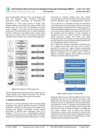
Volume: 04 Issue: 06 | June -2017 www.irjet.net p-ISSN: 2395-0072
© 2017, IRJET | Impact Factor value: 5.181 | ISO 9001:2008 Certified Journal | Page 1321
IC DESIGN PHYSICAL VERIFICATION
Vikram Gautam1, Dr. Pawan Kumar Dahiya2
1M.Tech. student in ECE (VLSI Design)
2Assistant Professor of Electronics & Communication Department,
1,2Deenbandhu Chhotu Ram University of Science and Technology, Sonepat, India
------------------------------------------------------------------------***-------------------------------------------------------------------------
Abstract— This paper will discuss how physical
verification flow optimized in IC Design having various
rule decks from foundries. Objective is to avoid delay and
reduce time to tape-out. With increased number of design
rules, design complexity and size of the designed chip run
time and memory used drastically increased. Number of
solutions presented to check design violations during
physical verification. DRC (design rule check), LVS (layout
vs. schematic), and XRC (extraction) are most crucial and
important milestones considered for chip making. Since
multiple foundries present different process for design
tape-outs, flow depends on foundry to check turnaround
time and the physical verification process followed. Time
to market depends on the design and verification as well,
physical verification is most critical since it is last stage
before design on silicon.
Key Words: VLSI, Physical verification, DRC, LVS, XRC,
Design flow
1. INTRODUCTION
While in the digital domain many design steps have been
automated through synthesis algorithms attempts to
apply such methods in analog design typically fail due to
the number and complexity of design constraints that
typically emerge from analog circuits. This work
presents a practical automation method for IC design
assembly using various automation methods for its
layout physical verification [1]. These methods can be
used along with design verification flow followed in the
verification as various violations encountered. Violations
are encountered at various stages of verification to
automate the determined solution layouts generated.
The presented concept shows an enhanced way of
verification automation by considering designs for layout
versus schematic issues, in order to generate the
possible solution for entire circuit, hierarchically
consisting of other designs as well as their
interconnections. This approach has two vital objectives:
first to extensively include designer’s human expertise,
knowledge and creativity into the automation, and
second to take only small automation steps which
enhance the design flow in verification stage [7]. A basic
overview of previous design automation techniques
evolved in the digital and analog domain. The idea of
employing the isolation with respect to different layout
objects interacting at top level and the implementation
based on schematic guided layout. The objective is to
have the functionality observed in the schematic is as
such reflecting in the layout.
Physical verification tool has to do layout processing &
proximity correction comprising rule files for
manufacturing. Runtime depends on size of the layout &
rules to be checked with increasing complexity of
designs. The operation of a circuit by means of
reenactments at the schematic level before endeavoring
to design is confirmed. LVS verifies the schematic and
layout match, so if schematic is not functioning properly
layout would not either. Passing LVS at lower levels of
hierarchy reduces time and effort at later stages. Any
change in schematic or layout requires re-run of LVS
tool. Recent improvement in the tools doesn’t require re-
run of the LVS tool, but in the same job can be checked
against the changes made in the layout.
Fig -1: Physical verification top view [8]
Fig. 1 shows how the problem in layout physical
verification is resolved using several commands running
to produce error output and modified layout (where
physical verification for layout modification is used for
optimal correction). Turnaround time is reduced to
extent possible by using optimal processing platform to
determine the command run and part of the layout
subject to change, and these combinations used as
separate blocks for processing. The results reassembled
at the end can be generalised [2].
2. BACKGROUND
EDA tools with sign-off checks are used to perform
physical verification on the layout before tape out.
Number of iterative steps involved in fixing the problems](https://image.slidesharecdn.com/irjet-v4i6244-180131105927/85/IC-Design-Physical-Verification-1-320.jpg)
![International Research Journal of Engineering and Technology (IRJET) e-ISSN: 2395 -0056
Volume: 04 Issue: 06 | June -2017 www.irjet.net p-ISSN: 2395-0072
© 2017, IRJET | Impact Factor value: 5.181 | ISO 9001:2008 Certified Journal | Page 1321
IC DESIGN PHYSICAL VERIFICATION
Vikram Gautam1, Dr. Pawan Kumar Dahiya2
1M.Tech. student in ECE (VLSI Design)
2Assistant Professor of Electronics & Communication Department,
1,2Deenbandhu Chhotu Ram University of Science and Technology, Sonepat, India
------------------------------------------------------------------------***-------------------------------------------------------------------------
Abstract— This paper will discuss how physical
verification flow optimized in IC Design having various
rule decks from foundries. Objective is to avoid delay and
reduce time to tape-out. With increased number of design
rules, design complexity and size of the designed chip run
time and memory used drastically increased. Number of
solutions presented to check design violations during
physical verification. DRC (design rule check), LVS (layout
vs. schematic), and XRC (extraction) are most crucial and
important milestones considered for chip making. Since
multiple foundries present different process for design
tape-outs, flow depends on foundry to check turnaround
time and the physical verification process followed. Time
to market depends on the design and verification as well,
physical verification is most critical since it is last stage
before design on silicon.
Key Words: VLSI, Physical verification, DRC, LVS, XRC,
Design flow
1. INTRODUCTION
While in the digital domain many design steps have been
automated through synthesis algorithms attempts to
apply such methods in analog design typically fail due to
the number and complexity of design constraints that
typically emerge from analog circuits. This work
presents a practical automation method for IC design
assembly using various automation methods for its
layout physical verification [1]. These methods can be
used along with design verification flow followed in the
verification as various violations encountered. Violations
are encountered at various stages of verification to
automate the determined solution layouts generated.
The presented concept shows an enhanced way of
verification automation by considering designs for layout
versus schematic issues, in order to generate the
possible solution for entire circuit, hierarchically
consisting of other designs as well as their
interconnections. This approach has two vital objectives:
first to extensively include designer’s human expertise,
knowledge and creativity into the automation, and
second to take only small automation steps which
enhance the design flow in verification stage [7]. A basic
overview of previous design automation techniques
evolved in the digital and analog domain. The idea of
employing the isolation with respect to different layout
objects interacting at top level and the implementation
based on schematic guided layout. The objective is to
have the functionality observed in the schematic is as
such reflecting in the layout.
Physical verification tool has to do layout processing &
proximity correction comprising rule files for
manufacturing. Runtime depends on size of the layout &
rules to be checked with increasing complexity of
designs. The operation of a circuit by means of
reenactments at the schematic level before endeavoring
to design is confirmed. LVS verifies the schematic and
layout match, so if schematic is not functioning properly
layout would not either. Passing LVS at lower levels of
hierarchy reduces time and effort at later stages. Any
change in schematic or layout requires re-run of LVS
tool. Recent improvement in the tools doesn’t require re-
run of the LVS tool, but in the same job can be checked
against the changes made in the layout.
Fig -1: Physical verification top view [8]
Fig. 1 shows how the problem in layout physical
verification is resolved using several commands running
to produce error output and modified layout (where
physical verification for layout modification is used for
optimal correction). Turnaround time is reduced to
extent possible by using optimal processing platform to
determine the command run and part of the layout
subject to change, and these combinations used as
separate blocks for processing. The results reassembled
at the end can be generalised [2].
2. BACKGROUND
EDA tools with sign-off checks are used to perform
physical verification on the layout before tape out.
Number of iterative steps involved in fixing the problems](https://image.slidesharecdn.com/irjet-v4i6244-180131105927/75/IC-Design-Physical-Verification-1-2048.jpg)
![International Research Journal of Engineering and Technology (IRJET) e-ISSN: 2395 -0056
Volume: 04 Issue: 06 | June -2017 www.irjet.net p-ISSN: 2395-0072
© 2017, IRJET | Impact Factor value: 5.181 | ISO 9001:2008 Certified Journal | Page 1323
Fig -4: Verification flow for analog design
4. CONCLUSION
Designs are getting larger and complex day by day, time
for physical designs schedule continuing same or
shorter. Verification is continuous process regarding
flow automation because rule files are subject to change
from time to time based on foundries. Runset might get
Confluence with the updated runset in order to obtain
necessary adjustments based on automation of flow. As
advancements observed in technology, older versions of
EDA tools might not be useful and new features in tools
need to cater latest problems in deep submicron
technologies. Different EDA tools might be different from
each other in flow automation. Hence new structure
demand development in the flow from time to time. Fully
automation in design and verification is still not practical
in complex design constraints. The main objective is to
avoid the delayed tape out.
5. REFERENCES
[1] Rebecca M. C. Roberts and Coenrad J. Fourie,
“Layout-to-Schematic as a Step Towards Layout-
Versus-Schematic Verification of SFQ Integrated
Circuit Layouts,” International Scholarly and
Scientific Research & Innovation, vol 9, IEEE 2015.
[2] Rahul Kapoor, Marilyn Adan and Louis Schaffer,
“Achieving Optimal Performance Scalability for
Physical Verification,” Synopsys, Inc. 2004.
[3] Ahmed Arafa, Hend Wagieh, Rami Fathy, John
Ferguson, Doug Morgan, Mohab Anis and Mohamed
Dessouky, “Schematic-Driven Physical Verification:
Fully Automated Solution for Analog IC design,”
Mentor Graphics Corporation, IEEE 2012.
[4] Elango Velayuthamt, “Accelerating Physical
Verification with an In Design Flow,” Synopsys, Inc.
May 2009.
[5] Paul Friedberg, “In-Design Physical Verification-
Automatic DRC Repair (ADR),” Synopsys, Inc. March
2011.
[6] https://www.mentor.com/solutions/foundry/
[7] Z. Nian and D. C. Wunsch, “Speeding up VLSI layout
verification usingfuzzy attributed graphs approach,”
IEEE Trans. Fuzzy Syst., vol. 14, no. 6, pp. 728–737,
Dec. 2006.
[8] H. S. Baird and Y. E. Cho, “An artwork design
verification system,” in Proc. 12th Des. Autom. Conf.,
1975, pp. 414–420.
[9] E. Barke, “A network comparison algorithm for
layout verification of integrated circuits,” IEEE
Trans. Comput.-Aided Design Integr. Circuits Syst.,
vol. CAD-3, no. 2, pp. 135–141, Apr. 1984.
[10] M. Ohlrich, C. Ebeling, E. Ginting, and L. Sather,
“SubGemini: Identifying SubCircuits using a fast
subgraph isomorphism algorithm,” in Proc. 30th Des.
Autom. Conf., Jun. 1993, pp. 31–37.
[11] R. M. C. Roberts and C. J. Fourie, “Layout-to-
schematic as a step towards layout-versus-schematic
verification of SFQ integrated circuit layouts,” in
Proc. AFRICON, Pointe-Aux-Piments, Mauritius,
2013, pp. 898–902.](https://image.slidesharecdn.com/irjet-v4i6244-180131105927/85/IC-Design-Physical-Verification-3-320.jpg)

This document discusses the physical verification process for integrated circuit (IC) design. Physical verification involves design rule checking (DRC), layout versus schematic (LVS) checking, and extraction (XRC) to check for errors before manufacturing. As designs increase in complexity and size, the runtime and memory usage of physical verification tools also increases drastically. The document outlines the different stages of physical verification flows for both digital and analog designs. It emphasizes that physical verification is a crucial last stage before fabrication, and that delays at this stage can negatively impact the time to market. Automating parts of the physical verification process can help reduce turnaround times and catch errors earlier.


