Download to read offline
![02/10/2020 GDDR5 SDRAM - Wikipedia
https://en.wikipedia.org/wiki/GDDR5_SDRAM 1/5
GDDR5 SDRAM
GDDR5 SDRAM, an abbreviation for Graphics Double Data Rate 5 Synchronous Dynamic Random-
Access Memory, is a modern type of synchronous graphics random-access memory (SGRAM) with a high
bandwidth ("double data rate") interface designed for use in graphics cards, game consoles, and high-
performance computing.[1] It is a type of GDDR SDRAM (graphics DDR SDRAM).
Overview
Commercialization of GDDR5
GDDR5X
GDDR5X commercialization
See also
References
External links
Like its predecessor, GDDR4, GDDR5 is based on DDR3 SDRAM memory, which has double the data lines
compared to DDR2 SDRAM. GDDR5 also uses 8-bit wide prefetch buffers similar to GDDR4 and DDR3
SDRAM.
GDDR5 SGRAM conforms to the standards which were set out in the GDDR5 specification by the JEDEC.
SGRAM is single-ported. However, it can open two memory pages at once, which simulates the dual-port
nature of other VRAM technologies. It uses an 8N-prefetch architecture and DDR interface to achieve high
performance operation and can be configured to operate in ×32 mode or ×16 (clamshell) mode which is
detected during device initialization. The GDDR5 interface transfers two 32-bit wide data words per write
clock (WCK) cycle to/from the I/O pins. Corresponding to the 8N-prefetch, a single write or read access
consists of a 256-bit wide two CK clock cycle data transfer at the internal memory core and eight
corresponding 32-bit wide one-half WCK clock cycle data transfers at the I/O pins.
GDDR5 operates with two different clock types. A differential command clock (CK) as a reference for address
and command inputs, and a forwarded differential write clock (WCK) as a reference for data reads and writes,
that runs at twice the CK frequency. Being more precise, the GDDR5 SGRAM uses a total of three clocks: two
write clocks associated with two bytes (WCK01 and WCK23) and a single command clock (CK). Taking a
GDDR5 with 5 Gbit/s data rate per pin as an example, the CK runs with 1.25 GHz and both WCK clocks at
2.5 GHz. The CK and WCKs are phase aligned during the initialization and training sequence. This alignment
allows read and write access with minimum latency.
A single 32-bit GDDR5 chip has about 67 signal pins and the rest are power and grounds in the 170 BGA
package.
Contents
Overview
Commercialization of GDDR5](https://image.slidesharecdn.com/gddr5sdram-wikipedia-201003190510/85/GDDR5-SDRAM-Notes-1-320.jpg)
![02/10/2020 GDDR5 SDRAM - Wikipedia
https://en.wikipedia.org/wiki/GDDR5_SDRAM 1/5
GDDR5 SDRAM
GDDR5 SDRAM, an abbreviation for Graphics Double Data Rate 5 Synchronous Dynamic Random-
Access Memory, is a modern type of synchronous graphics random-access memory (SGRAM) with a high
bandwidth ("double data rate") interface designed for use in graphics cards, game consoles, and high-
performance computing.[1] It is a type of GDDR SDRAM (graphics DDR SDRAM).
Overview
Commercialization of GDDR5
GDDR5X
GDDR5X commercialization
See also
References
External links
Like its predecessor, GDDR4, GDDR5 is based on DDR3 SDRAM memory, which has double the data lines
compared to DDR2 SDRAM. GDDR5 also uses 8-bit wide prefetch buffers similar to GDDR4 and DDR3
SDRAM.
GDDR5 SGRAM conforms to the standards which were set out in the GDDR5 specification by the JEDEC.
SGRAM is single-ported. However, it can open two memory pages at once, which simulates the dual-port
nature of other VRAM technologies. It uses an 8N-prefetch architecture and DDR interface to achieve high
performance operation and can be configured to operate in ×32 mode or ×16 (clamshell) mode which is
detected during device initialization. The GDDR5 interface transfers two 32-bit wide data words per write
clock (WCK) cycle to/from the I/O pins. Corresponding to the 8N-prefetch, a single write or read access
consists of a 256-bit wide two CK clock cycle data transfer at the internal memory core and eight
corresponding 32-bit wide one-half WCK clock cycle data transfers at the I/O pins.
GDDR5 operates with two different clock types. A differential command clock (CK) as a reference for address
and command inputs, and a forwarded differential write clock (WCK) as a reference for data reads and writes,
that runs at twice the CK frequency. Being more precise, the GDDR5 SGRAM uses a total of three clocks: two
write clocks associated with two bytes (WCK01 and WCK23) and a single command clock (CK). Taking a
GDDR5 with 5 Gbit/s data rate per pin as an example, the CK runs with 1.25 GHz and both WCK clocks at
2.5 GHz. The CK and WCKs are phase aligned during the initialization and training sequence. This alignment
allows read and write access with minimum latency.
A single 32-bit GDDR5 chip has about 67 signal pins and the rest are power and grounds in the 170 BGA
package.
Contents
Overview
Commercialization of GDDR5](https://image.slidesharecdn.com/gddr5sdram-wikipedia-201003190510/75/GDDR5-SDRAM-Notes-1-2048.jpg)
![02/10/2020 GDDR5 SDRAM - Wikipedia
https://en.wikipedia.org/wiki/GDDR5_SDRAM 2/5
GDDR5 was revealed by Samsung Electronics in July 2007. They announced that they would mass-produce
GDDR5 starting in January 2008.[2]
Hynix Semiconductor introduced the industry's first 60 nm class "1 Gb" (10243 bit) GDDR5 memory in
2007.[3] It supported a bandwidth of 20 GB/s on a 32-bit bus, which enables memory configurations of 1 GB at
160 GB/s with only 8 circuits on a 256-bit bus. The following year, in 2008, Hynix bested this technology with
its 50 nm class "1 Gb" GDDR5 memory.
In November 2007, Qimonda, a spin-off of Infineon, demonstrated and sampled GDDR5,[4] and released a
paper about the technologies behind GDDR5.[5] As of May 10, 2008, Qimonda announced volume production
of 512 Mb GDDR5 components rated at 3.6 Gbit/s (900 MHz), 4.0 Gbit/s (1 GHz), and 4.5 Gbit/s
(1.125 GHz).[6]
On November 20, 2009, Elpida Memory announced the opening of the company's Munich Design Center,
responsible for Graphics DRAM (GDDR) design and engineering. Elpida received GDDR design assets from
Qimonda AG in August 2009 after Qimonda's bankruptcy. The design center has approximately 50 employees
and is equipped with high-speed memory testing equipment for use in the design, development and evaluation
of Graphics memory.[7][8] On July 31, 2013, Elpida became a fully owned subsidiary of Micron Technology
and based on current public LinkedIn professional profiles, Micron continues to operate the Graphics Design
Center in Munich.[9][10]
Hynix 40 nm class "2 Gb" (2 × 10243 bit) GDDR5 was released in 2010. It operates at 7 GHz effective clock-
speed and processes up to 28 GB/s.[11][12] "2 Gb" GDDR5 memory chips will enable graphics cards with 2 GB
or more of onboard memory with 224 GB/s or higher peak bandwidth. On June 25, 2008, AMD became the
first company to ship products using GDDR5 memory with its Radeon HD 4870 video card series,
incorporating Qimonda's 512 Mb memory modules at 3.6 Gbit/s bandwidth.[13][14]
In June 2010, Elpida Memory announced the company's 2 Gb GDDR5 memory solution, which was developed
at the company's Munich Design Center. The new chip can work at up to 7 GHz effective clock-speed and will
be used in graphics cards and other high bandwidth memory applications.[15]
"4 Gb" (4 × 10243 bit) GDDR5 components became available in the third quarter of 2013. Initially released by
Hynix, Micron Technology quickly followed up with their implementation releasing in 2014. On February 20,
2013, it was announced that the PlayStation 4 will use sixteen 4 Gb GDDR5 memory chips for a total of 8 GB
of GDDR5 @ 176 Gbit/s (CK 1.375 GHz and WCK 2.75 GHz) as combined system and graphics RAM for use
with its AMD-powered system on a chip comprising 8 Jaguar cores, 1152 GCN shader processors and AMD
TrueAudio.[16] Product teardowns later confirmed the implementation of 4 Gb based GDDR5 memory in the
PlayStation 4.[17][18]
In February 2014, as a result of its acquisition of Elpida, Micron Technology added 2 Gb and 4 Gb GDDR5
products into the company's portfolio of graphics memory solutions.[19]
As of January 15, 2015, Samsung announced in a press release that it had begun mass production of "8 Gb" (8
× 10243 bits) GDDR5 memory chips based on a 20 nm fabrication process. To meet the demand of higher
resolution displays (such as 4K) becoming more mainstream, higher density chips are required in order to
facilitate larger frame buffers for graphically intensive computation, namely PC gaming and other 3D
rendering. Increased bandwidth of the new high-density modules equates to 8 Gbit/s per pin × 170 pins on the
BGA package x 32-bits per I/O cycle, or 256 Gbit/s effective bandwidth per chip.[20]
On January 6, 2015, Micron Technology President Mark Adams announced the successful sampling of 8 Gb
GDDR5 on the company's fiscal Q1-2015 earnings call.[21][22] The company then announced, on January 25,
2015, that it had begun commercial shipments of GDDR5 using a 20 nm process technology.[23][24][25] The
GDDR5X](https://image.slidesharecdn.com/gddr5sdram-wikipedia-201003190510/85/GDDR5-SDRAM-Notes-2-320.jpg)
![02/10/2020 GDDR5 SDRAM - Wikipedia
https://en.wikipedia.org/wiki/GDDR5_SDRAM 3/5
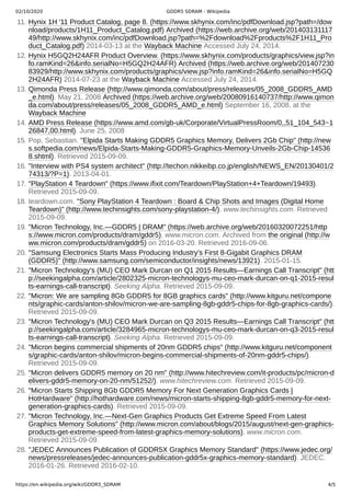
formal announcement of Micron's 8 Gb GDDR5 appeared in the form of a blog post (http://www.micron.com/a
bout/blogs/2015/august/next-gen-graphics-products-get-extreme-speed-from-latest-graphics-memory-solutions)
by Kristopher Kido on the company's website September 1, 2015.[26][27]
In January 2016, JEDEC standardized GDDR5X SGRAM.[28] GDDR5X targets a transfer rate of 10 to 14
Gbit/s per pin, twice that of GDDR5.[29] Essentially, it provides the memory controller the option to use either a
double data rate mode that has a prefetch of 8n, or a quad data rate mode that has a prefetch of 16n.[30] GDDR5
only has a double data rate mode that has an 8n prefetch.[31] GDDR5X also uses 190 pins per chip (190
BGA).[30] By comparison, standard GDDR5 has 170 pins per chip; (170 BGA).[31] It therefore requires a
modified PCB.
Micron Technology began sampling GDDR5X chips in March 2016,[32] and began mass production in May
2016.[33]
Nvidia officially announced the first graphics card using GDDR5X, the Pascal-based GeForce GTX 1080 on
May 6, 2016.[34] Later, the second graphics card to use GDDR5X, the Nvidia Titan X on July 21, 2016,[35] the
GeForce GTX 1080 Ti on February 28, 2017,[36] and Nvidia Titan Xp on April 6, 2017.[37]
List of device bit rates
1. Micron TN-ED-01: GDDR5 SGRAM Introduction. (https://www.micron.com/~/media/documents/pr
oducts/technical-note/dram/tned01_gddr5_sgram_introduction.pdf) Accessed April 11, 2014
2. Pancescu, Alexandru (July 18, 2007). "Samsung Pushes The GDDR5 Standard Forward" (https://
news.softpedia.com/news/Samsung-Pushes-The-GDDR5-Standard-Forward-60237.shtml).
Softpedia. Retrieved 18 September 2019.
3. "History: 2000s" (https://www.skhynix.com/eng/about/history2000.jsp). SK Hynix. Retrieved 8 July
2019.
4. Register report (http://www.reghardware.co.uk/2007/11/01/qimonda_samples_gddr5) Archived (ht
tps://web.archive.org/web/20080706004800/http://www.reghardware.co.uk/2007/11/01/qimonda_
samples_gddr5) 2008-07-06 at the Wayback Machine. Retrieved November 2, 2007.
5. Qimonda GDDR5 (http://www.hwstation.net/img/news/allegati/Qimonda_GDDR5_whitepaper.pdf)
White Paper
6. GDDR5 in Production, New Round of Graphics Cards War Imminent. (http://www.xbitlabs.com/ne
ws/video/display/20080510113121_GDDR5_in_Production_New_Round_of_Graphics_Cards_W
ar_Imminent.html), retrieved May 11, 2008
7. Topalov, Milan. "Elpida officially opens Munich Design Center" (http://www.fabtech.org/news/_a/el
pida_officially_opens_munich_design_center/). www.fabtech.org. Retrieved 2015-09-09.
8. "Elpida Opens High Speed DRAM Test Laboratory at Munich Design Center | Business Wire" (htt
p://www.businesswire.com/news/home/20091119006409/en/Elpida-Opens-High-Speed-DRAM-Te
st-Laboratory#.VfCxfpeb8ec). www.businesswire.com. Retrieved 2015-09-09.
9. "Micron (MU) Completes Elpida Memory, Rexchip Purchases" (http://www.streetinsider.com/Corp
orate+News/Micron+%2528MU%2529+Completes+Elpida+Memory,+Rexchip+Purchases/85499
56.html). Retrieved 2015-09-09.
10. "Markus Balb | LinkedIn" (http://www.linkedin.com/pub/markus-balb/ab/289/311/en).
GDDR5X commercialization
See also
References](https://image.slidesharecdn.com/gddr5sdram-wikipedia-201003190510/85/GDDR5-SDRAM-Notes-3-320.jpg)

GDDR5 SDRAM, a type of synchronous graphics memory, is designed for high-performance graphics cards and computing with a high bandwidth DDR interface. It was introduced in 2007 and saw significant advancements in data rates and production, including the development of GDDR5X, which offers even higher transfer rates. GDDR5 has become integral in modern graphics hardware, including applications in gaming consoles like the PlayStation 4.