Downloaded 29 times


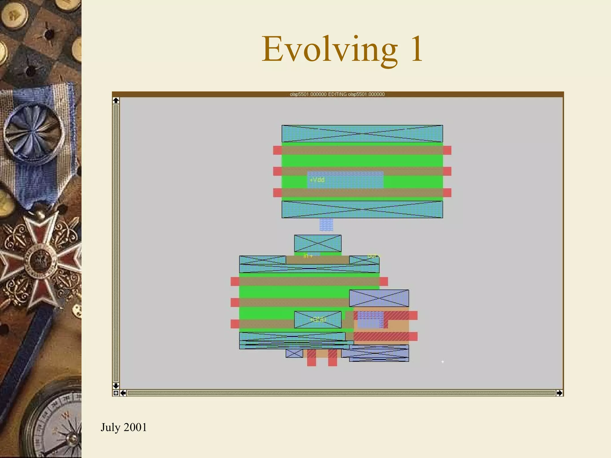
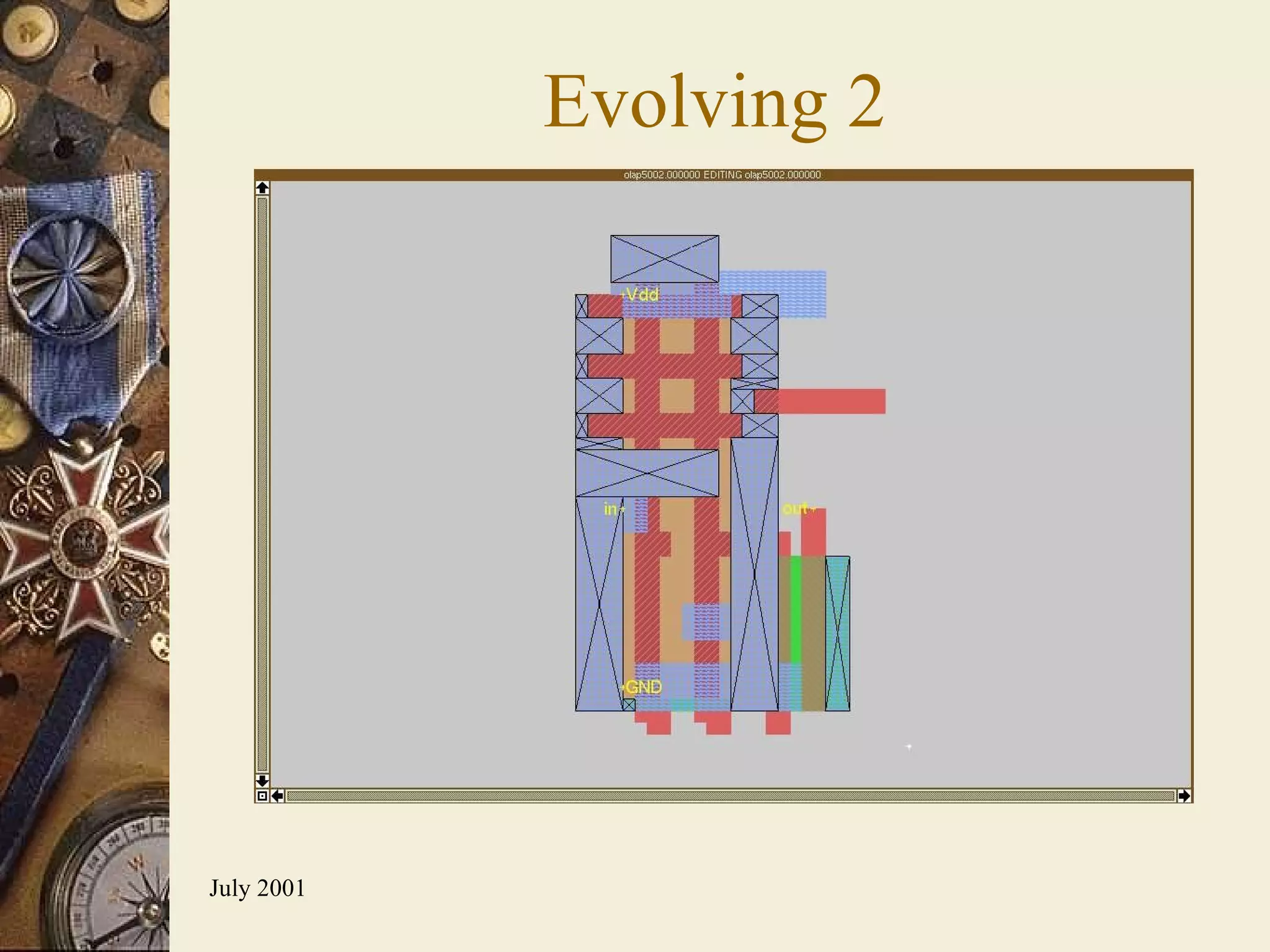
![Limitations Does not always find the best solution – Is this acceptable? Presently unable to design more complex cells Alternative representation Starting from similar designs Speed – almost linear speedup [Mazumder]](https://image.slidesharecdn.com/ga-vlsi-100903232904-phpapp02/75/Example-of-Automating-Transistor-level-Design-36-2048.jpg)

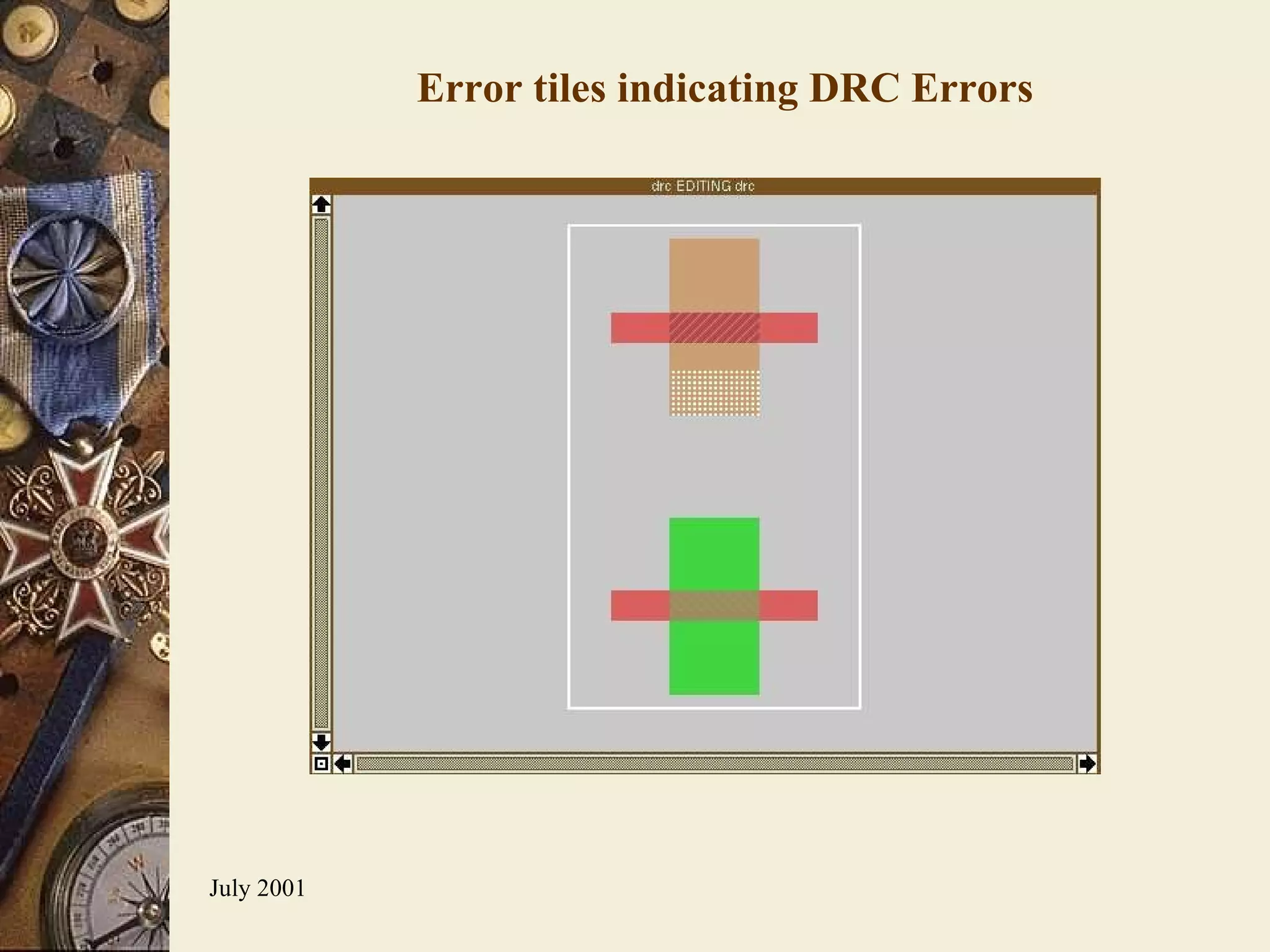
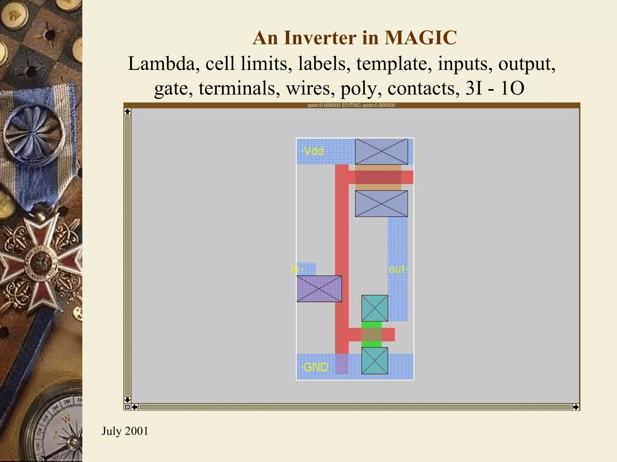
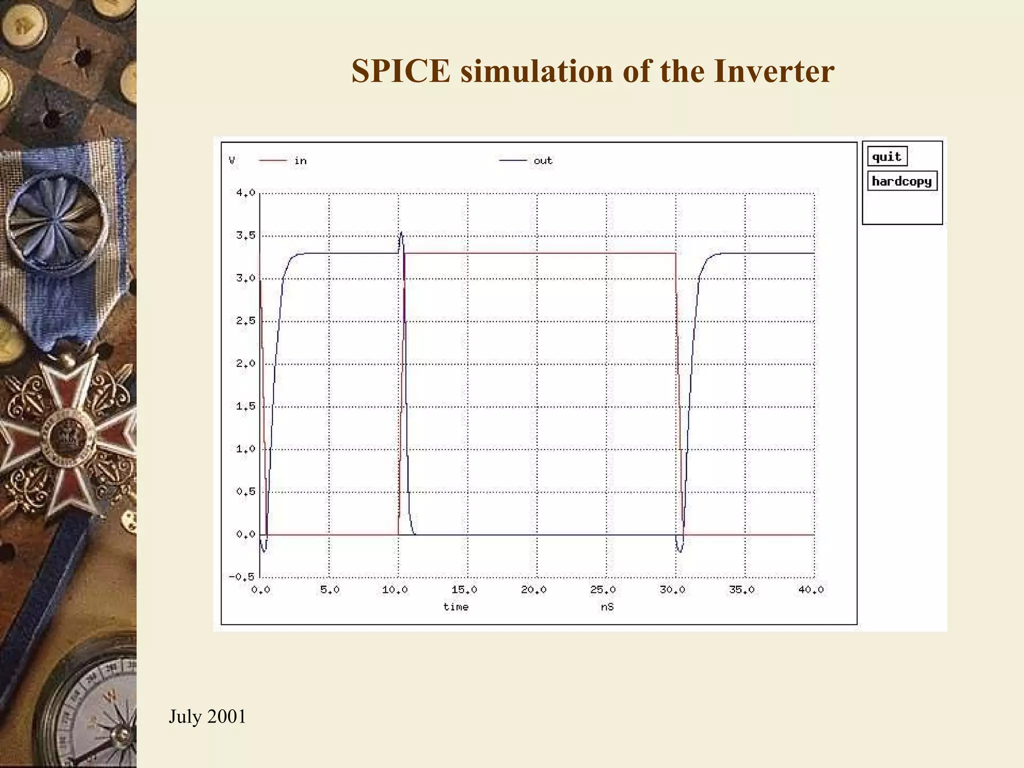
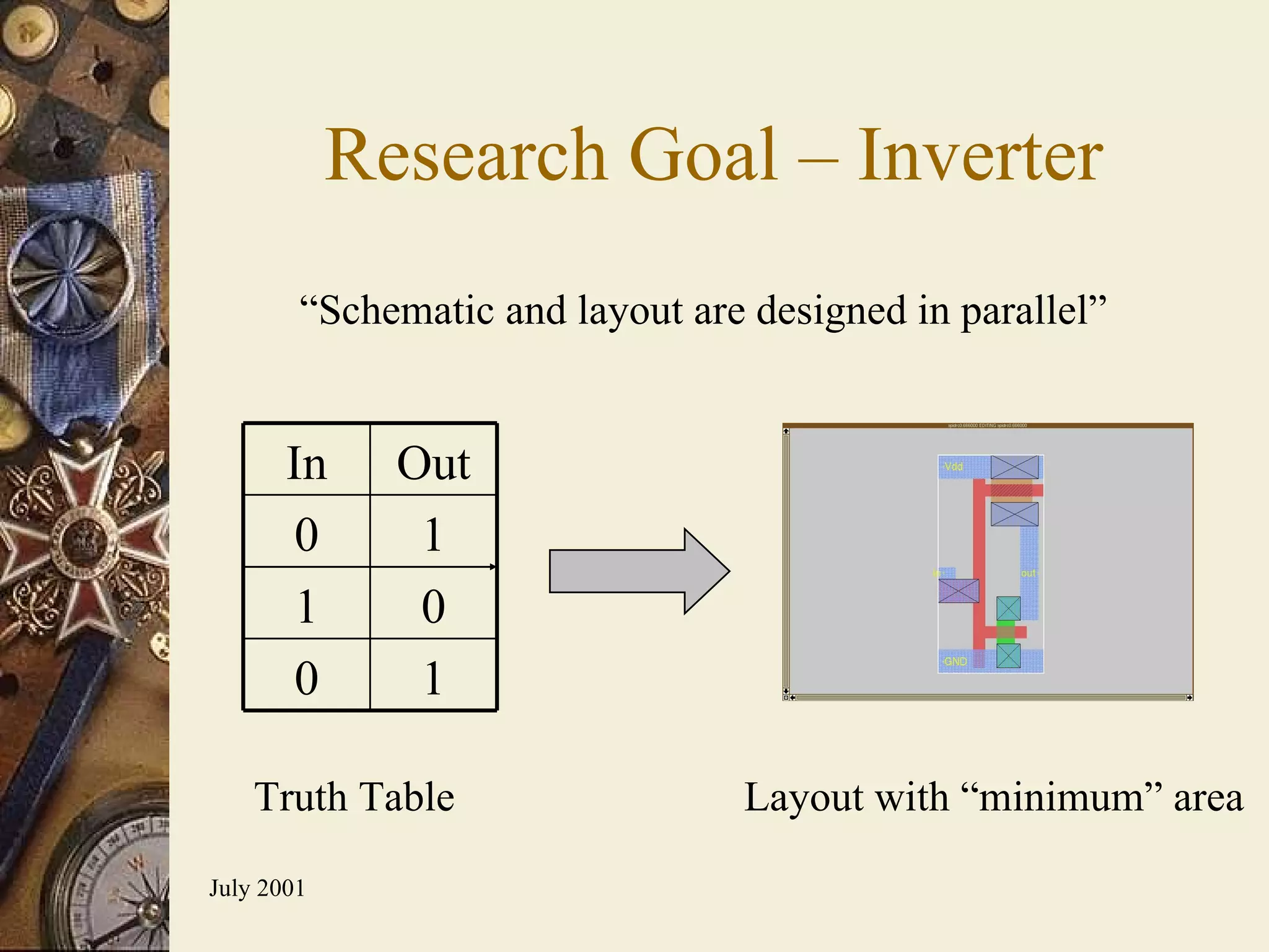
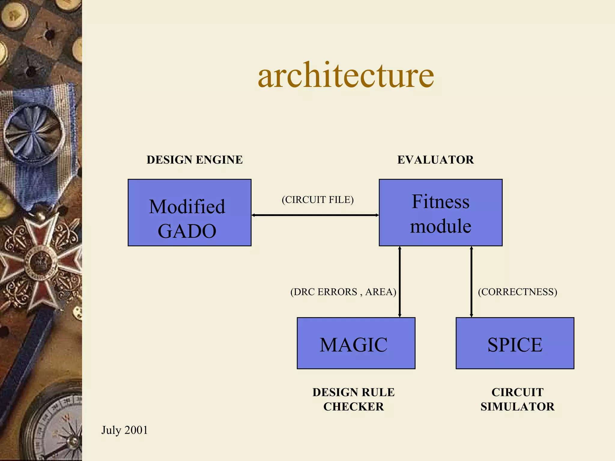
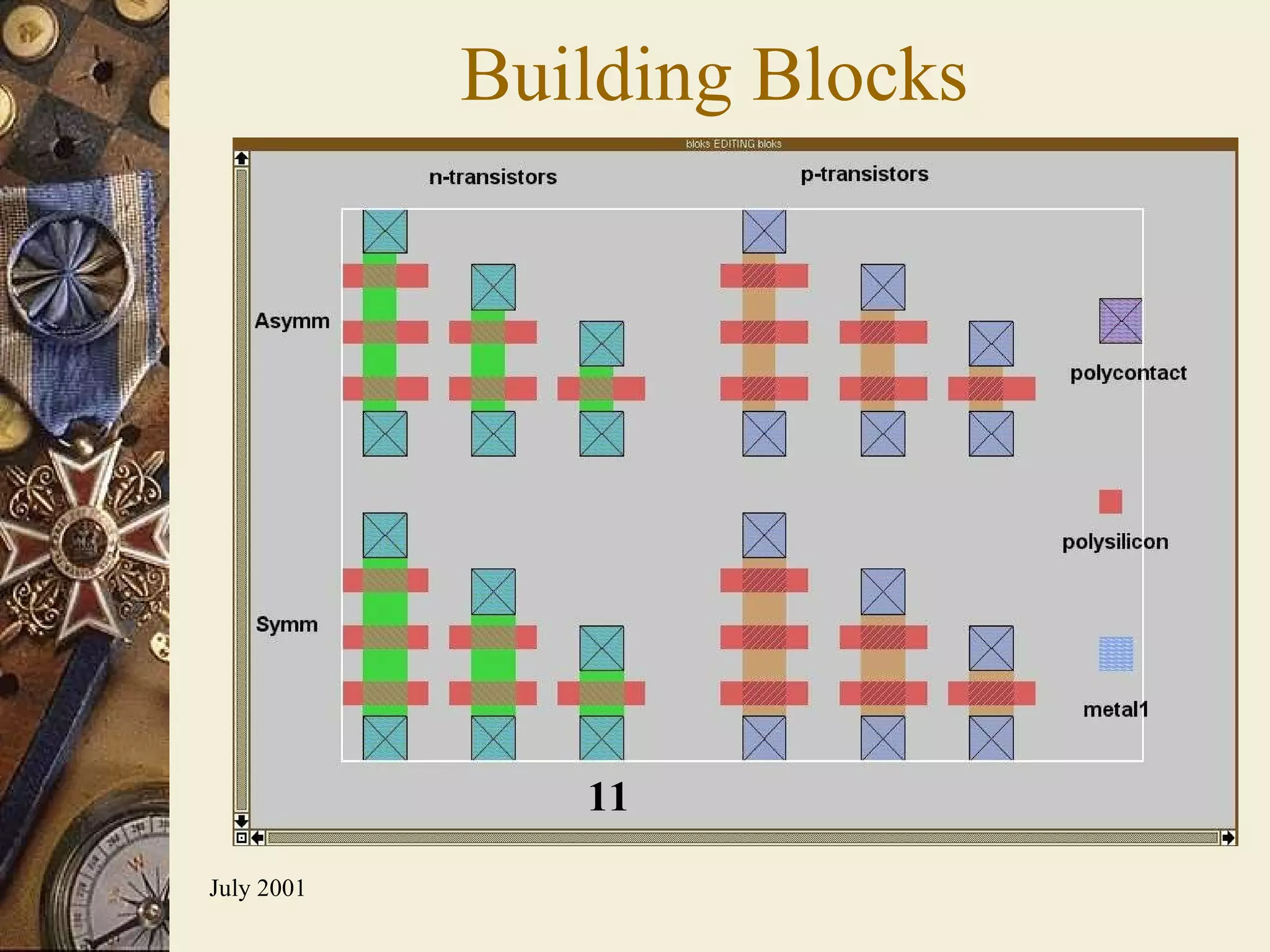
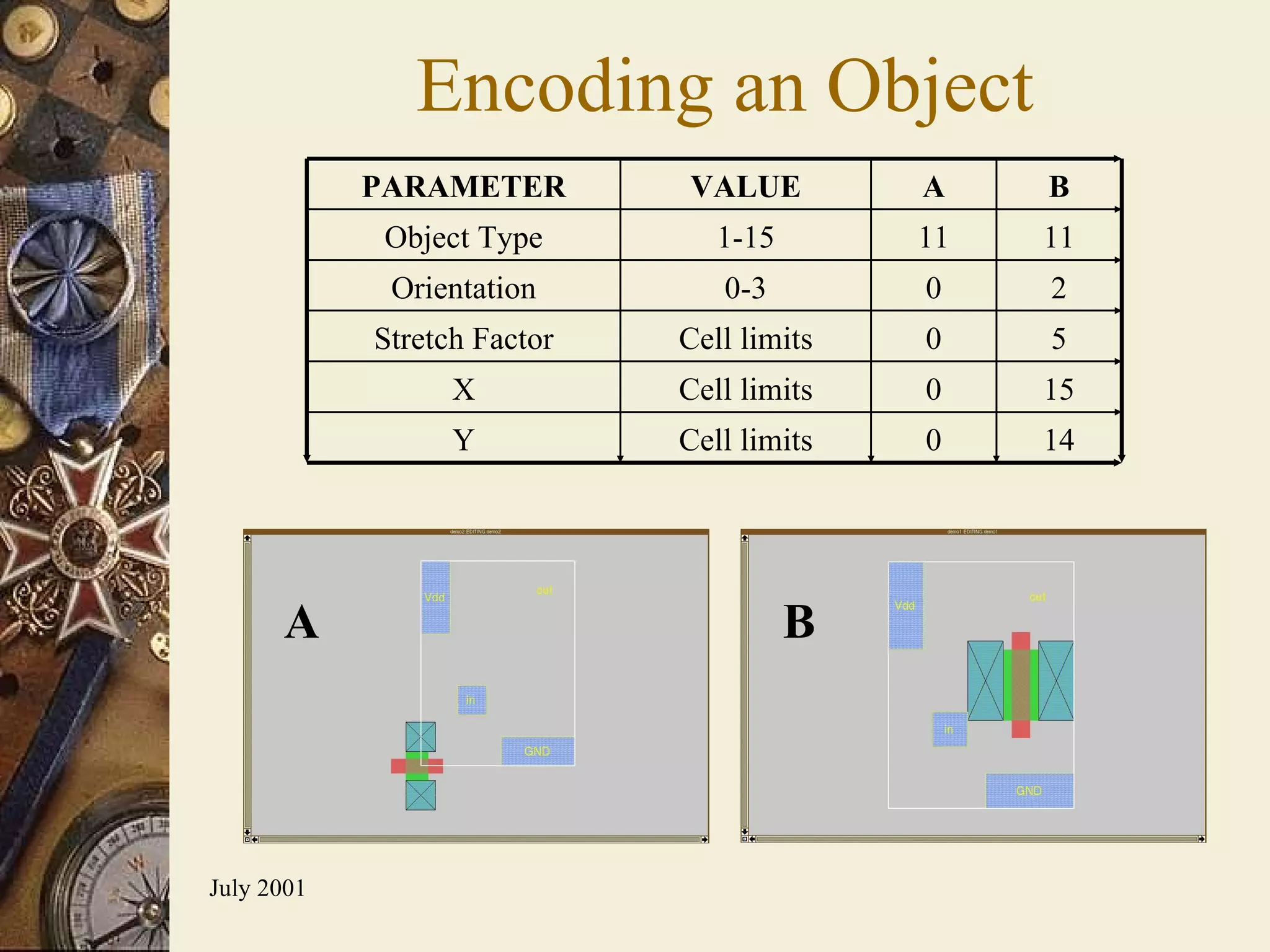
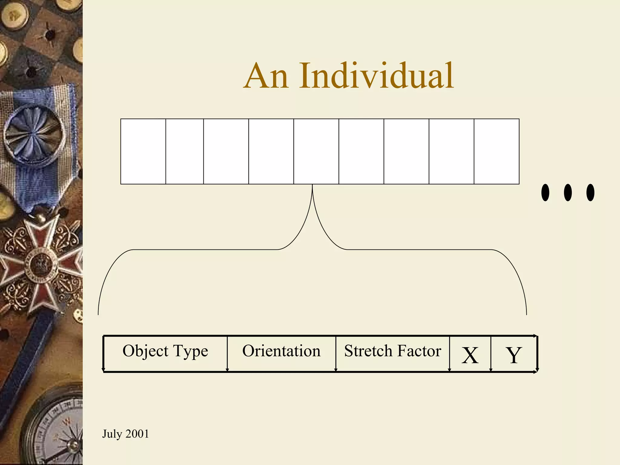
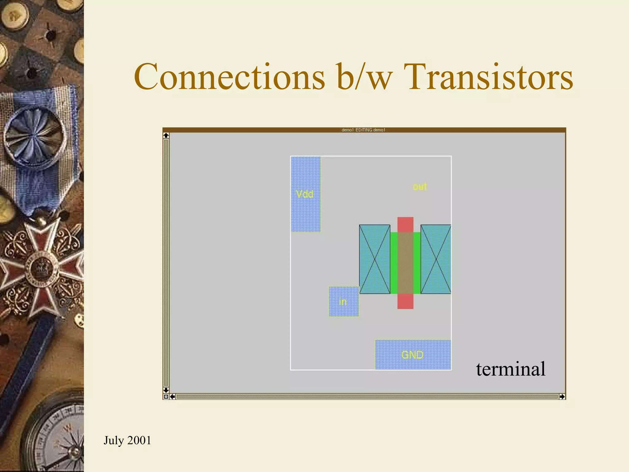
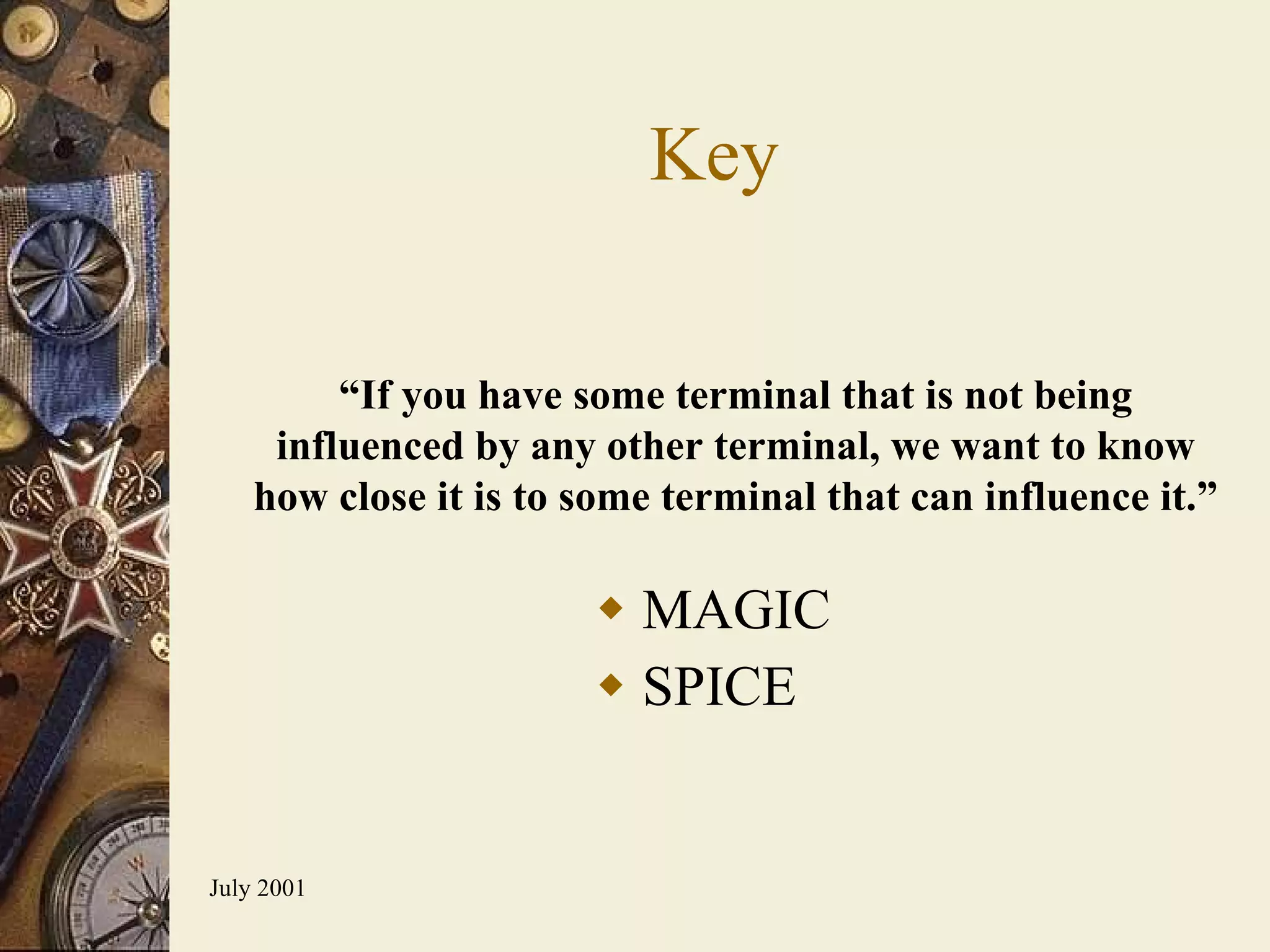
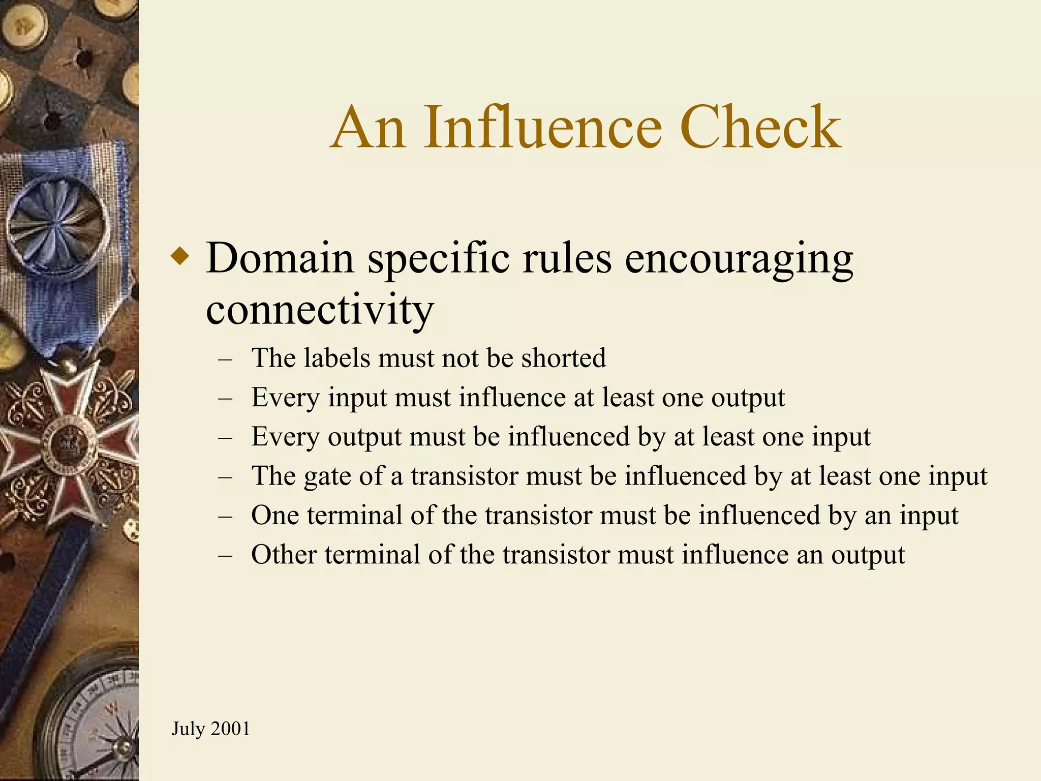
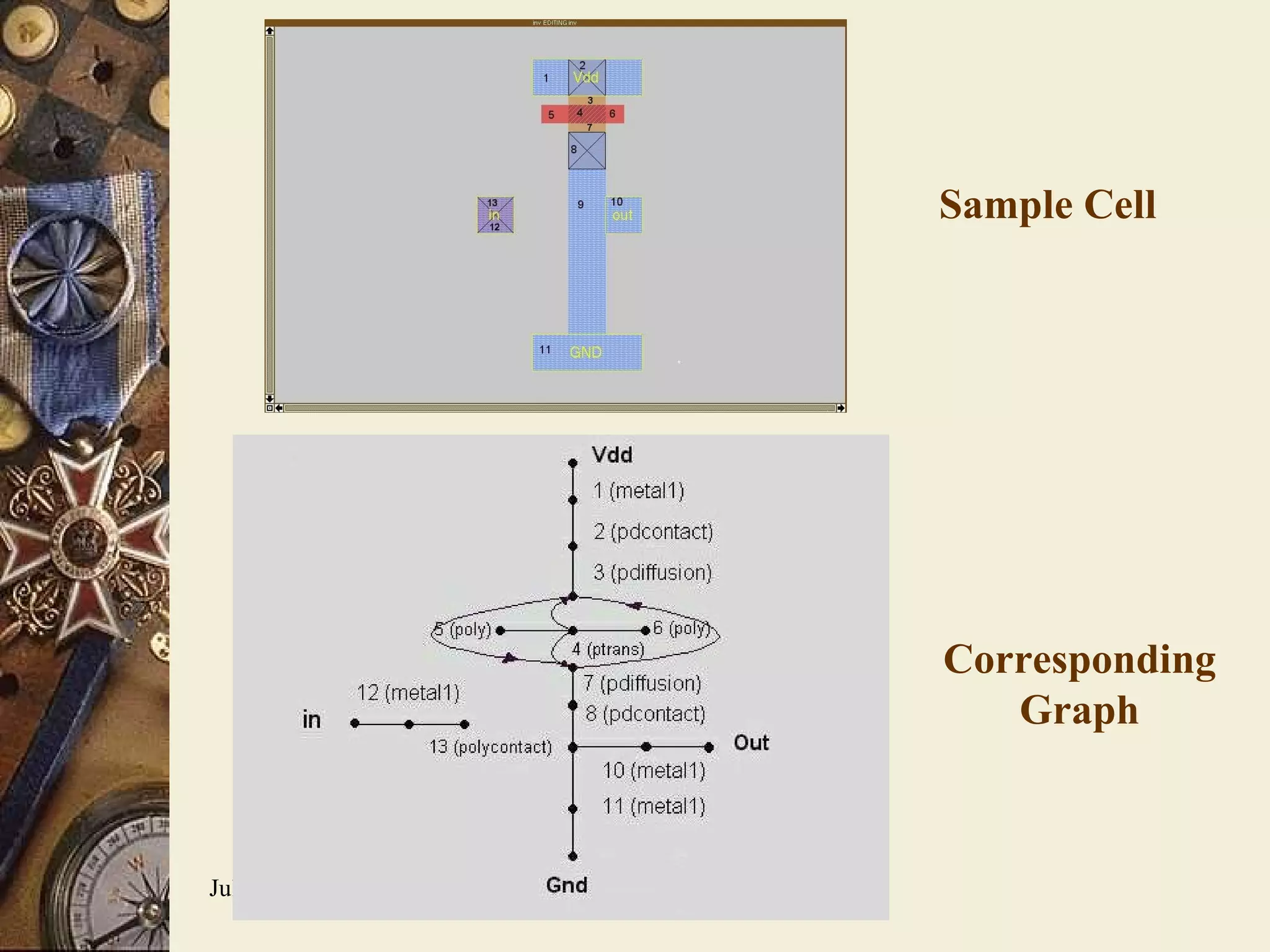
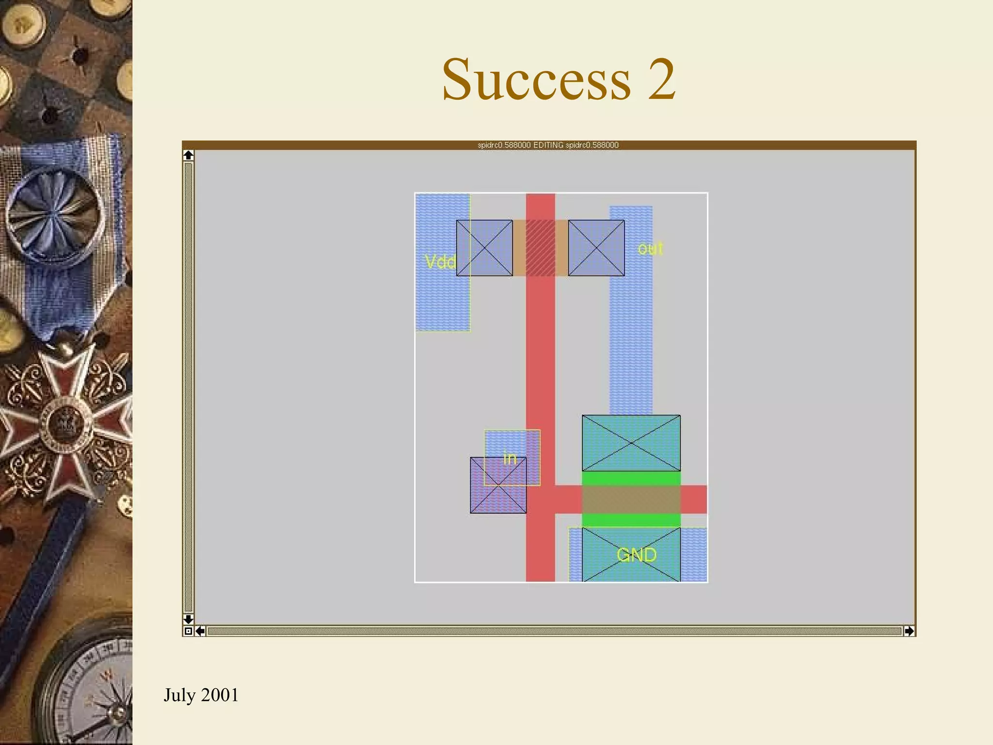
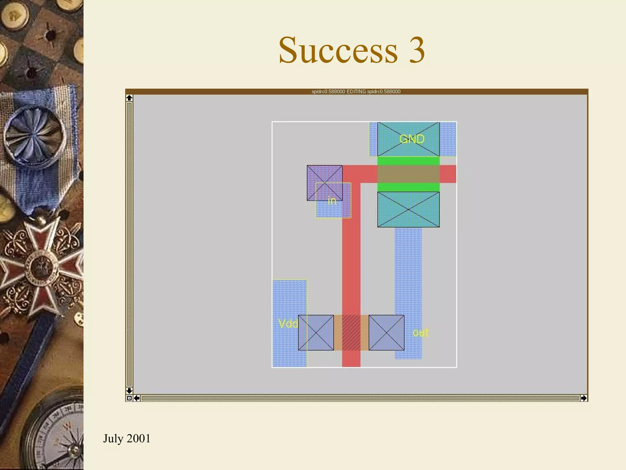
The document discusses an evolutionary approach to standard cell design aimed at automating the design process to reduce costs and time associated with creating essential building blocks of VLSI chips. It highlights the challenges of traditional design methods and presents a new methodology for generating layouts in parallel with schematics. The research emphasizes the importance of fitness functions in evaluating design correctness and connectivity while acknowledging current limitations in handling complex designs.