Download to read offline
![International Journal of VLSI design & Communication Systems (VLSICS) Vol.3, No.2, April 2012
DOI : 10.5121/vlsic.2012.3212 133
FAULT SECURE ENCODER AND DECODER
WITH CLOCK GATING
N.Kapileswar1
and P.Vijaya Santhi2
Dept.of ECE,NRI Engineering College, Pothavarapadu,,,INDIA
1
nvkapil@gmail.com, 2
santhipalepu@gmail.com
Abstract:
This paper presents circuit design for a low power fault secure encoder and decoder system. Memory cells
in logic circuits have been protected from soft errors for more than a decade due to increase in soft error
rates. In this paper the circuitry around the memory block have been susceptible to soft errors and must be
protected from faults. The proposed design uses error correcting codes and ring counter addressing
scheme. In the ring counter several new clock gating techniques are proposed to reduce power
consumption. A fault secure Encoder and Decoder error free low power logic circuits can be achieved by
the proposed design. Simulation results show great improvement in power consumption. Fault secure
Encoder and Decoder with clock gated by CG-element consumes approximately half the power of that
consumed by the fault free circuit which doesn’t employ clock gating technique
Keywords:
GC-element, first-in–first-out (FIFO), gated-clock, ring-counter, Double edge triggered(DET ) D flip-
flop(DFF ), encoder, decoder, detector, corrector.
1.1 Introduction
Communication devices have experienced explosive growth recently. Longer battery life and
fault free operation are crucial factors in the widespread success of these products. Low power
design is followed for fault free circuits. Error rate is more in logic circuits. Most of the logic
circuits consist of memory. From past ten years, all researchers concentrated in memory cells.
They designed circuits to reduce faults in memory[11,13]. Even though the memory cells are
protected, the error rate is not reduced to an appreciable level. Then the concentration is moved
on to the surrounding circuitries of the memory to reduce error rate [11,13]. In most of the logic
circuits at the transmitter end and at the receiver end, encoder and decoder circuits are observed.
In this paper the surrounding circuitries of memory cells are encoder block and decoder block.
To reduce error rate in logic circuits a fault secure encoder and decoder is needed [11,13]. On
adding fault secure design to existing encoder and decoder circuit will increase power
consumption. Power consumption has become one of the biggest challenges in high-performance
logic circuit design. Designers are thus continuously challenged to come up with innovative ways
to reduce power[4], while trying to meet all the other constraints imposed on the design. So, the
idea is to design a fault secure encoder and decoder with clock gating technique. Clock gating is
one of the power reduction technique. The idea of clock gating is to shut down the clock of any
component whenever it is not being used (accessed). It involves inserting combinational logic
along the clock path to prevent the unnecessary switching of sequential elements. The deigned](https://image.slidesharecdn.com/3212vlsics12-181015084943/85/FAULT-SECURE-ENCODER-AND-DECODER-WITH-CLOCK-GATING-1-320.jpg)
![International Journal of VLSI design & Communication Systems (VLSICS) Vol.3, No.2, April 2012
134
circuit reduce error rate and also consumes less power. The existing circuit is just a encoder and
decoder with out any fault secure system. The data is stored in memory address generated by
binary address decoder. Memory system which can tolerate errors in any part of the system,
including the storage unit, encoder and decoder. The information bits are fed into the encoder to
encode the information vector. At the output of encoder, error may occur in the code word. The
error should be detected and corrected before storing it in memory. The code word is then stored
in the memory. Later during operation, the stored code word will be retrieved from the memory
unit. Since the code word is susceptible to transient faults while it is stored in the memory, or
retrieving the code word. Before decoding the code word, errors should corrected, otherwise the
decoded information is not same as the transmitted information. There is need to add detector
and corrector circuitry to both encoder and decoder to reduce error rate. To reduce error rate in
logic circuits a fault secure encoder and decoder is needed. On adding fault secure design to
existing encoder and decoder circuit will increase power consumption.
1.2 Clock gating:
The idea of clock gating is to shut down the clock of any component whenever it is not being
used (accessed).on inserting combinational logic along the clock path the unnecessary switching
of sequential elements are prevented. Now a days Power consumption has become one of the
biggest challenges in high-performance logic circuit design. Designers are thus continuously
challenged to come up with innovative ways to reduce power, while trying to meet all the other
constraints imposed on the design. Clock gating has been used to reduce dynamic clock power
through all levels of the design hierarchy from the top-most chip level down to the individual
latch level .On increasing the circuitry in clock path power consumption is reduced. If there is
no need of switching some elements in the circuit, then clock is not supplied to those elements.
Main concentration is on clock signal because major consumption of power is by clock signal.
2.1 Implementation of fault Secure Encoder and Decoder with clock
gating.
Memory system which can tolerate errors in any part of the system, including the storage unit,
encoder and corrector circuit, using the fault-secure detector is shown below. There is a fault
secure detector that can detect any combination of errors in the received code word along with
errors in the detector circuit. This fault secure detector can verify the correctness of the encoder
and corrector operation[11,13]. To address memory, ring counter is used[3]. This ring counter
employs clock gating technique to reduce power consumption. An overview of the proposed fault
secure encoder and decoder with clock gating is shown in fig. 1, and is as described below.](https://image.slidesharecdn.com/3212vlsics12-181015084943/85/FAULT-SECURE-ENCODER-AND-DECODER-WITH-CLOCK-GATING-2-320.jpg)
![International Journal of VLSI design & Communication Systems (VLSICS) Vol.3, No.2, April 2012
135
Figure1. Block diagram of fault secure encoder and decoder with clock gating
The information bits are fed into the encoder to encode the information vector, and the fault
secure detector of the encoder verifies the validity of the encoded vector. If the detector detects
any error, the encoding operation must be redone to generate the correct code word. The code
word is then stored in the memory by address generated by ring counter. The ring counter
employs clock gating techniques. Later during operation, the stored code word will be retrieved
from the memory unit. Since the code word is susceptible to transient faults while it is stored in
the memory, the retrieved code-word must be fed into the detector to detect any potential error
and possibly to the corrector to recover any erroneous bits. The circuit designed consumes less
power and is a fault secure system
2.2 Design Structure of Encoder
An n-bit code-word c, which encodes k-bit information vector i is generated by multiplying the k-
bit information vector with k × n bit generator matrix G, i.e.,
c = i · G. Fig.2 shows the generator matrix of (15, 7) code. All the rows of the matrix are cyclic
shifts of the first row. This cyclic code generation does not generate a systematic code and the
information bits must be decoded from the encoded vector, which is not desirable for our fault-
tolerant approach due to the further complication and delay that it adds to the operation[2].
C0c1c2 c3 c4 c5 c6 c7 c8 c9c10c11c12c13c14
I0 1 0 0 0 1 0 1 1 1 0 0 0 0 0 0
I1 0 1 0 0 0 1 0 1 1 1 0 0 0 0 0
I2 0 0 1 0 0 0 1 0 1 1 1 0 0 0 0
I3 0 0 0 1 0 0 0 1 0 1 1 1 0 0 0
I4 0 0 0 0 1 0 0 0 1 0 1 1 1 0 0
I5 0 0 0 0 0 1 0 0 0 1 0 1 1 1 0
I6 0 0 0 0 0 0 1 0 0 0 1 0 1 1 1
Figure 2. The generator matrix of code (15, 7) in cyclic format](https://image.slidesharecdn.com/3212vlsics12-181015084943/85/FAULT-SECURE-ENCODER-AND-DECODER-WITH-CLOCK-GATING-3-320.jpg)
![International Journal of VLSI design & Communication Systems (VLSICS) Vol.3, No.2, April 2012
136
The generator matrix of any cyclic code can be converted into systematic form (G = [I : X]) The
encoded vector, which is generated by the inner product of the information vector and the
generator matrix, consists of information bits followed by parity bits, where each parity bit is
simply an inner product of information vector and a column of X, from G = [I : X].
2.3 Design structure of Fault Secure Detector
The core of the detector operation is to generate the syndrome vector, which is basically
implementing the following vector-matrix multiplication on the received encoded vector c and
parity-check matrix H. c T
H = S.
Figure 3. Fault-secure detector for (15, 7) code
Therefore each bit of the syndrome vector is the product of C with one row of the parity-check
matrix. This product is a linear binary sum over digits of C. where the corresponding digit in the
matrix row is 1. This binary sum is implemented with an XOR gate. Fig.3 shows the detector
circuit for the (15, 7) code. An error is detected if any of the syndrome bits has a nonzero value.
The final error detection signal is implemented by an OR function of all the syndrome bits. The
output of this r-input OR gate is the error detector signal.
2.4 Design structure of Ring counter with clock gated by R–S flip-flop
By observing the fact that only one of the DFFs in the ring counter is activated at any time, the
gated-clock technique has then been proposed to be applied to the DFFs. every eight DFFs in the
ring counter are grouped into one block. Then, a “gate” signal is computed for each block to gate
the frequently toggled clock signal when the block can be inactive so that unnecessary power
wasted in clock signal transitions is saved. The clock signal is gated by RS-flip flop.
Figure 4. Ring counter with clock gated by RS-flip flop](https://image.slidesharecdn.com/3212vlsics12-181015084943/85/FAULT-SECURE-ENCODER-AND-DECODER-WITH-CLOCK-GATING-4-320.jpg)
![International Journal of VLSI design & Communication Systems (VLSICS) Vol.3, No.2, April 2012
140
Systems
Power
Consumption
(mW)
Clock
frequency
(MHz)
Delay
time
(nsec)
Supply
voltage
(volts)
Without clock gating 105 60 4.990 2.5
Clock gated by RS-flip
flop
107 60 4.950 2.5
Clock gated by CG-
element
57 60 4.670 2.5
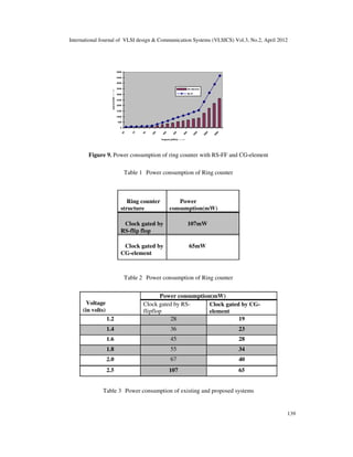
By observing Table 1, Table 2 and Table 3, proposed system with clock gated by CG-element
consumes less power than the system with out clock gating and also clock gated by RS-flip flop.
For supply voltage of 2.5v and at frequency of 60 MHz, fault secure encoder and decoder
without clock gating consumes 105mW of power, with clock gated by RS-flip flop consumes
107 mW and with clock gated by CG-element consumes 57mW of power. The proposed system
consumes less power and also has less delay time. The optimum frequency is 60 MHz for the
designed system. An important observation from Table 3 is system clock gated by RS-flip flop
consumes more power than the system without clock gating because the extra RS-flip flops still
serve as loading of the clock signal and demand more than necessary clock power.
3.2 Conclusion
An efficient circuit to reduce soft error’s in logic circuits is designed. Proposed system with
clock gated by CG-element consumes less power than the system without clock gating and also
clock gated by RS-flip flop. For supply voltage 2.5v and at frequency of 60 MHz, fault secure
encoder and decoder without clock gating consumes 105mW of power, with clock gated by RS-
flip flop consumes 107 mW and with clock gated by CG-element consumes 57mW of power.
The proposed system consumes less power and also has less delay time. The optimum frequency
is 60 MHz for the designed system. The system clock gated by RS-flip flop consumes more
power than the system without clock gating because the extra RS-flip flops still serve as loading
of the clock signal and demand more than necessary clock power. The proposed technique can be
used in low power circuit design for multimedia communication devices where long battery life
is a crucial factor.
3.3 References
[1] Gallager R.G, “Low-Density Parity-Check Codes”. Cambridge, MA:MIT Press, 1963
[2] McEliece R.J, “The Theory of Information and Coding”. Cambridge, U.K.: Cambridge University
Press, 2002.
[3] Tsern.E K and Meng T. H, “A low-power video-rate pyramid VQ decoder,” IEEE J. Solid-State
Circuits, Vol. 31, No. 11, Nov. 1996, pp. 1789–1794.
[4] Po-Chun Hsieh, Jing-Siang Jhuang, Pei-Yun Tsai, “A Low-Power Delay Buffer Using Gated Driver
Tree” IEEE Trans. Very Large Scale Integr. (VLSI) Syst.,Vol. 17, No. 9, Sep. 2009.
[5] Hosain R, Wronshi L. D, and albicki A, “Low power design using double edge triggered flip-flop,”
IEEE Trans. Very Large Scale Integr. (VLSI ) Syst., Vol. 2, No. 2, Jun. 1994 pp. 261–265.](https://image.slidesharecdn.com/3212vlsics12-181015084943/85/FAULT-SECURE-ENCODER-AND-DECODER-WITH-CLOCK-GATING-8-320.jpg)
![International Journal of VLSI design & Communication Systems (VLSICS) Vol.3, No.2, April 2012
141
[6] Pastuszak G, “A high-performance architecture for embedded block coding in JPEG 2000,” IEEE
Trans. Circuits Syst. Video Technol., Vol. 15, No. 9, Sep. 2005, pp. 1182–1191.
[7] Ryan W. E, “An Introduction to LDPC Codes”, in CRC Handbook for Coding and Signal Processing
for Recording Systems (Ed. B. Vasic), CRC Press, 2004.
[8] Karkooti M, Cavallaro J.R, “Semi-Parallel Reconfigurable Architectures for Real-Time LDPC
Decoding”, ITCC 2004.
[9] Zhong H, Zhang T, “Design of VLSI Implementation-Oriented LDPC Codes”, IEEE Semiannual
Vehicular Technology Conference (VTC), Oct. 2003.
[10] Yeo E, Nikolic B, and Anantharam V, “Architectures and Implementations of Low-Density Parity
Check Decoding Algorithms”, IEEE International Midwest Symposium on Circuits and Systems,
August. 2002.
[11] Naeimi H and DeHon A, “Fault secure encoder and decoder for memory applications,” in Proc. IEEE
Int. Symp. Defect Fault Tolerance VLSI Syst., Sep. 2007, pp. 409–417.
[12] Howard S.L, Gaudet V.C, and Schlegal C, “Soft-Bit Decoding of Regular Low-Density Parity Check
Codes”, IEEE Transactions on Circuits and Systems.
[13] Naeimi H and DeHon A, “Fault-tolerant nano-memory with fault secure encoder and decoder,”
presented at the Int. Conf. Nano-Netw., Catania, Sicily, Italy, Sep. 2007.
[14] Piestrak S. J, Dandache A, and Monteiro F, “Designing fault-secure parallel encoders for systematic
linear error correcting codes,” IEEE Trans. Reliab., vol. 52, no. 4, Jul. 2003, pp. 492–500.
.[15] Lin S and Costello D. J, “Error Control Coding”, 2nd ed. Englewood Cliffs, NJ: Prentice-Hall, 2004.](https://image.slidesharecdn.com/3212vlsics12-181015084943/85/FAULT-SECURE-ENCODER-AND-DECODER-WITH-CLOCK-GATING-9-320.jpg)

This paper presents a low power fault secure encoder and decoder system designed to protect against soft errors in memory circuits using error correcting codes and clock gating techniques. The proposed design significantly reduces power consumption, achieving approximately half the power usage compared to non-clock gated systems, while ensuring fault tolerance. Simulation results confirm the effectiveness of the design, highlighting a reduction in power consumption and delay time.