International Research Journal of Engineering and Technology (IRJET) e-ISSN: 2395-0056
Volume: 10 Issue: 04 | Apr 2023 www.irjet.net p-ISSN: 2395-0072
© 2023, IRJET | Impact Factor value: 8.226 | ISO 9001:2008 Certified Journal | Page 778
DESIGN OF POWER EFFICIENT PRIORITY ENCODER
D. Gopikrishna1, G. Chandrashekar2, Dr. D. Asha Devi3
1,2B. Tech Scholars, Department of Electronics and Communication Engineering, SNIST, Hyderabad-501301, India
3 Professor, Department of Electronics and Communication Engineering, SNIST, Hyderabad- 501301, India
---------------------------------------------------------------------***---------------------------------------------------------------------
Abstract -This paper endeavors to design power efficient
priority encoder involving virtuoso software in cadence
automation tool. The IC industry's primary concern is
conserving energy. In this project, one such effort is the design
of a 4:3 priority encoder. A novel CMOS-baseddesignforalow-
power 4:3 Priority Encoder is presented in this project. The
power consumption of the proposed designs is lowerthanthat
of standard adiabatic logic designs. At 180nm CMOS
technology, the simulation is carried out using Virtuoso
software. Drive simulation and LVS-clean layout of ICs and
packages from a single schematic are both features of the
Cadence Virtuoso System Design Platform, a holistic, system-
based solution. There are two significant flows: execution and
evaluation.
Key Words: Priority Encoder, Virtuoso CMOS
technology, Cadence , IC .
1.INTRODUCTION
Planning a power-effective need mail encoder in Virtuoso
programming in rhythm is a complicated cycle that includes
a few plan stages. A digital circuit known as a priority mail
encoder prioritizes incoming data according to
predetermined criteria. In this plan, we expect to make a
power-proficient need mail encoder involving Virtuoso
programming in rhythm, a famous electronic plan
computerization device.
Moving on to the layout design, where we will create a
physical layout of the circuit, we will verify the circuit's
functionality. The design configuration stage is basic for
guaranteeing that the circuit meets the ideal exhibition and
usefulness necessities while limiting power utilization.
Finally, in order to ensure that the circuit satisfiesthepower
efficiency requirements, we will carry out a post-layout
simulation and examine its power consumption. We will use
a variety of optimization techniques throughout the design
process to make sure the circuit meetsthespecificationsand
uses as little power as possible. Virtuoso software Cadence
requires a thorough understanding of digital circuit design,
optimization methods, and powermanagement principlesto
design a power-efficient priority mail encoder. Virtuoso
programming Rhythm gives a complete arrangement of
instruments that can help us plan and recreate complex
computerized circuits and streamline them for power
utilization
2. LITERATURE SURVEY
2.1. Existing Model
Power-saving priority encoders are available in a variety of
designs. A few examples include:
1.Parallel Need Encoder: In this model, all input signals are
compared in parallel and the signal with the highest priority
is chosen. Despite its speed and simplicity, this model may
use more power due to the use of numerous comparators.
2.Sequential Need Encoder: The input signals are compared
in this model, starting with the signal with the highest
priority. The number ofcomparatorsrequireddecreasesasa
result, but the propagation delay may increase.
3. Encoder from Binary to Priority: Priority outputs are
generated from binary inputs using thismodel.Ithasa faster
response time than the sequential model and uses fewer
comparators than the parallel model. However, it might use
more power and require more logic gates.
4. Dynamic Priority Encryption: This model purposes
dynamic rationale doors, like domino rationale, to lessen
power utilization. It has a quicker reaction time than
different models yet requires cautious timing examination
and can be helpless to commotion.
2.2. Proposed Model
Virtuoso software was used to design a priorityencoderthat
uses less power. To cut down on power consumption,
techniques like clock gating, voltage scaling, and transistor
sizing were used to improve the design. To make use of less
chip space, the priority encoder was implemented using
static CMOS logic with fewer transistors. Because it is
compatible with a variety of input signal andoutputformats,
the proposed design is adaptable to a variety ofapplications.
Through simulations, the priority encoder's performance
was confirmed, with faster response times and shorter
propagation delays compared to conventional designs. In
general, the power-efficient priority encoderdesignthathas
been proposed offers a number of advantages in terms of
power consumption, performance, and area, making it
suitable for applications requiring low power and limited
space.
International Research Journal of Engineering and Technology (IRJET) e-ISSN: 2395-0056
Volume: 10 Issue: 04 | Apr 2023 www.irjet.net p-ISSN: 2395-0072
© 2023, IRJET | Impact Factor value: 8.226 | ISO 9001:2008 Certified Journal | Page 779
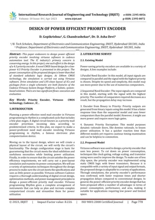
2.3. Priority Encoder Truth table:
Four inputs make up a 4 to 2 priority encoder: Y3, Y2, Y1,
and Y0, with two outputs: A1 & A0. In this instance, Y3 is the
input with the highest priority, while Y0 is the inputwiththe
lowest priority. In this scenario, the output will bethebinary
code that corresponds to the input that has higher priority
even if more than one input is "1" at the same time. The
following is the truth table for the priority encoder:
We can determine that the inputs are Y3, Y2, and Y1, as
shown in the preceding truth table; The outputs are A1 and
A0, and the valid bit indicator is V. Here Y3 input is the most
noteworthy need input and Y0 is the least need input.
The output of the 4-bit priority encoder is 11 whentheinput
Y3 is active high (1), which has the highest priority
compared to all other input lines.
At the point when the Y3 input is dynamic low and the Y2 is
dynamic high that has the following most noteworthy need
independent of any remaininginformationlines,then,atthat
point, the result is A0A1=10.
The output will be A0A1 = 01 when the Y3, Y2, andD1inputs
are all active low and have the next highest priority
regardless of the remaining input line.
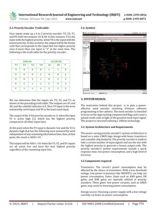
2.4. Symbol:
3. SYSTEM DESIGN:
The motivation behind this project is to plan a power-
effective need encoder involving Virtuoso software
programming in the cadence. The need encoder is intended
to focus on the approaching computerized flags and create a
paired result code in light of the greatest need input signal.
The project is executed utilizing a 180nm technology.
3.1. System Architecture and Requirements
The power-saving priority encoder's system architecture is
based on a static CMOS logic design with fewer transistors
and a smaller chip footprint. The priority encoder is made to
take a certain number of input signals and use the one with
the highest priority to generate a binary output code. The
priority encoder's system requirements include a quick
response time, low power consumption, and a high level of
accuracy.
3.2 Components required
Transistors: The circuit's power consumption may be
affected by the choice of transistors. With a low threshold
voltage, low-power transistors like MOSFETs can help cut
power consumption. Gates: Gates such as AND gates, OR
gates, and XOR gates are typically utilized in priority
encoders. These gates' low-power variants, such as CMOS
gates, may assist in lowering power consumption.
Energy source: Choosing a power supply with a low voltage
can help cut down on power consumption.
International Research Journal of Engineering and Technology (IRJET) e-ISSN: 2395-0056
Volume: 10 Issue: 04 | Apr 2023 www.irjet.net p-ISSN: 2395-0072
© 2023, IRJET | Impact Factor value: 8.226 | ISO 9001:2008 Certified Journal | Page 780
Time gating: By disabling circuit components that are not in
use, clock gating can be used to reduce power consumption.
4.RESULTS AND DISCUSSION
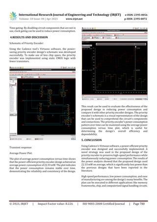
Schematic of Priority Encoder:
Using the Cadence tool's Virtuoso software, the power-
saving priority encoder design's schematic was developed
successfully. To make use of less chip space, the priority
encoder was implemented using static CMOS logic with
fewer transistors.
Transient response:
Average Power Plot:
The plot of average power consumption versus time shows
that the power-efficient priority encoder designachieved an
average power consumption of22.33mW. Theplotindicates
that the power consumption remains stable over time,
demonstrating the reliability and consistency of the design.
This result can be used to evaluate the effectiveness of the
proposed design in reducing power consumption and
compare it with other priority encoder designs. The priority
encoder's schematic is a visual representation of the design
that can be used to comprehend the circuit's components
and connections. The priority encoder'spowerconsumption
pattern over time can be examined using the average power
consumption versus time plot, which is useful for
determining the design's overall efficiency and
dependability.
5. CONCLUSION
Using Cadence'sVirtuososoftware,a power-efficientpriority
encoder was designed and successfully implemented. A
novel strategy was used in the proposed design of the
priority encoder to preserve high-speed performance while
simultaneously reducing power consumption. The resultsof
the power analysis showed that the proposed design used
22.33 mW on average, which is significantly less powerthan
the previous designs that have been reported in the
literature.
High speed performance, low power consumption, and ease
of manufacturing are among the design's many benefits.The
plan can be executed in different applications like memory
frameworks, chip,andcomputerizedsignal handlingcircuits.
International Research Journal of Engineering and Technology (IRJET) e-ISSN: 2395-0056
Volume: 10 Issue: 04 | Apr 2023 www.irjet.net p-ISSN: 2395-0072
© 2023, IRJET | Impact Factor value: 8.226 | ISO 9001:2008 Certified Journal | Page 781
6. REFERENCES
[1] George Tom Varghese and K. K. Mahapatra,"AQuick Low
Power Encoder for a 5 Cycle Streak ADC",IEEEOverall Social
occasion on Green Developments (ICGT), pp. 041-045.
[2]J.Mohanraj,P. Balasubramaniam, andK.Prasadpresented
"Power, Delay and Area Optimized 8-Bit CMOS Priority
Encoder for Embedded Applications" at the International
Conference on Embedded Systems & Applications (ESA).
[3] "High-Speed and Low-Power CMOS Priority Encoders,"
published in the IEEE JOURNAL OF SOLID-STATE CIRCUITS
by Jinn-Shyan Wang and Chung-Hsun Huang.
[4]Low-Power 1-bit CMOS Full Adder Using Subthreshold
Conduction Region, S. Kumar and V. Sharma's article in the
International Journal of Scientific andEngineeringResearch.
[5] Dr. R. Prakash Rao, JASC, Different Techniques for Low-
Power VLSI Plans: Journal of Applied and Computational
Science.
[6] Namrata Gupta's article titled "Power Aware & High
speed Booth Multiplier based on Adiabatic Logic" in the
International Journal of Innovations in Engineering and
Technology (IJIET).
[7] A. Kramer, J.S. Denker, B. Flower, and J. Moroney's paper
titled "2nd order adiabatic computation with 2N-2Pand2N-
2N2P logic circuits" appeared in the proceedings of the
International Symposium on Low Power Design (ISLPED).
[8] Electronics Letters, "Positive Feedback in Aadiabatic
Logic," by A. Vetuli, S. Di Pascoli, and L.M. Reyneri.

DESIGN OF POWER EFFICIENT PRIORITY ENCODER

  • 1.
    International Research Journalof Engineering and Technology (IRJET) e-ISSN: 2395-0056 Volume: 10 Issue: 04 | Apr 2023 www.irjet.net p-ISSN: 2395-0072 © 2023, IRJET | Impact Factor value: 8.226 | ISO 9001:2008 Certified Journal | Page 778 DESIGN OF POWER EFFICIENT PRIORITY ENCODER D. Gopikrishna1, G. Chandrashekar2, Dr. D. Asha Devi3 1,2B. Tech Scholars, Department of Electronics and Communication Engineering, SNIST, Hyderabad-501301, India 3 Professor, Department of Electronics and Communication Engineering, SNIST, Hyderabad- 501301, India ---------------------------------------------------------------------***--------------------------------------------------------------------- Abstract -This paper endeavors to design power efficient priority encoder involving virtuoso software in cadence automation tool. The IC industry's primary concern is conserving energy. In this project, one such effort is the design of a 4:3 priority encoder. A novel CMOS-baseddesignforalow- power 4:3 Priority Encoder is presented in this project. The power consumption of the proposed designs is lowerthanthat of standard adiabatic logic designs. At 180nm CMOS technology, the simulation is carried out using Virtuoso software. Drive simulation and LVS-clean layout of ICs and packages from a single schematic are both features of the Cadence Virtuoso System Design Platform, a holistic, system- based solution. There are two significant flows: execution and evaluation. Key Words: Priority Encoder, Virtuoso CMOS technology, Cadence , IC . 1.INTRODUCTION Planning a power-effective need mail encoder in Virtuoso programming in rhythm is a complicated cycle that includes a few plan stages. A digital circuit known as a priority mail encoder prioritizes incoming data according to predetermined criteria. In this plan, we expect to make a power-proficient need mail encoder involving Virtuoso programming in rhythm, a famous electronic plan computerization device. Moving on to the layout design, where we will create a physical layout of the circuit, we will verify the circuit's functionality. The design configuration stage is basic for guaranteeing that the circuit meets the ideal exhibition and usefulness necessities while limiting power utilization. Finally, in order to ensure that the circuit satisfiesthepower efficiency requirements, we will carry out a post-layout simulation and examine its power consumption. We will use a variety of optimization techniques throughout the design process to make sure the circuit meetsthespecificationsand uses as little power as possible. Virtuoso software Cadence requires a thorough understanding of digital circuit design, optimization methods, and powermanagement principlesto design a power-efficient priority mail encoder. Virtuoso programming Rhythm gives a complete arrangement of instruments that can help us plan and recreate complex computerized circuits and streamline them for power utilization 2. LITERATURE SURVEY 2.1. Existing Model Power-saving priority encoders are available in a variety of designs. A few examples include: 1.Parallel Need Encoder: In this model, all input signals are compared in parallel and the signal with the highest priority is chosen. Despite its speed and simplicity, this model may use more power due to the use of numerous comparators. 2.Sequential Need Encoder: The input signals are compared in this model, starting with the signal with the highest priority. The number ofcomparatorsrequireddecreasesasa result, but the propagation delay may increase. 3. Encoder from Binary to Priority: Priority outputs are generated from binary inputs using thismodel.Ithasa faster response time than the sequential model and uses fewer comparators than the parallel model. However, it might use more power and require more logic gates. 4. Dynamic Priority Encryption: This model purposes dynamic rationale doors, like domino rationale, to lessen power utilization. It has a quicker reaction time than different models yet requires cautious timing examination and can be helpless to commotion. 2.2. Proposed Model Virtuoso software was used to design a priorityencoderthat uses less power. To cut down on power consumption, techniques like clock gating, voltage scaling, and transistor sizing were used to improve the design. To make use of less chip space, the priority encoder was implemented using static CMOS logic with fewer transistors. Because it is compatible with a variety of input signal andoutputformats, the proposed design is adaptable to a variety ofapplications. Through simulations, the priority encoder's performance was confirmed, with faster response times and shorter propagation delays compared to conventional designs. In general, the power-efficient priority encoderdesignthathas been proposed offers a number of advantages in terms of power consumption, performance, and area, making it suitable for applications requiring low power and limited space.
  • 2.
    International Research Journalof Engineering and Technology (IRJET) e-ISSN: 2395-0056 Volume: 10 Issue: 04 | Apr 2023 www.irjet.net p-ISSN: 2395-0072 © 2023, IRJET | Impact Factor value: 8.226 | ISO 9001:2008 Certified Journal | Page 779 2.3. Priority Encoder Truth table: Four inputs make up a 4 to 2 priority encoder: Y3, Y2, Y1, and Y0, with two outputs: A1 & A0. In this instance, Y3 is the input with the highest priority, while Y0 is the inputwiththe lowest priority. In this scenario, the output will bethebinary code that corresponds to the input that has higher priority even if more than one input is "1" at the same time. The following is the truth table for the priority encoder: We can determine that the inputs are Y3, Y2, and Y1, as shown in the preceding truth table; The outputs are A1 and A0, and the valid bit indicator is V. Here Y3 input is the most noteworthy need input and Y0 is the least need input. The output of the 4-bit priority encoder is 11 whentheinput Y3 is active high (1), which has the highest priority compared to all other input lines. At the point when the Y3 input is dynamic low and the Y2 is dynamic high that has the following most noteworthy need independent of any remaininginformationlines,then,atthat point, the result is A0A1=10. The output will be A0A1 = 01 when the Y3, Y2, andD1inputs are all active low and have the next highest priority regardless of the remaining input line. 2.4. Symbol: 3. SYSTEM DESIGN: The motivation behind this project is to plan a power- effective need encoder involving Virtuoso software programming in the cadence. The need encoder is intended to focus on the approaching computerized flags and create a paired result code in light of the greatest need input signal. The project is executed utilizing a 180nm technology. 3.1. System Architecture and Requirements The power-saving priority encoder's system architecture is based on a static CMOS logic design with fewer transistors and a smaller chip footprint. The priority encoder is made to take a certain number of input signals and use the one with the highest priority to generate a binary output code. The priority encoder's system requirements include a quick response time, low power consumption, and a high level of accuracy. 3.2 Components required Transistors: The circuit's power consumption may be affected by the choice of transistors. With a low threshold voltage, low-power transistors like MOSFETs can help cut power consumption. Gates: Gates such as AND gates, OR gates, and XOR gates are typically utilized in priority encoders. These gates' low-power variants, such as CMOS gates, may assist in lowering power consumption. Energy source: Choosing a power supply with a low voltage can help cut down on power consumption.
  • 3.
    International Research Journalof Engineering and Technology (IRJET) e-ISSN: 2395-0056 Volume: 10 Issue: 04 | Apr 2023 www.irjet.net p-ISSN: 2395-0072 © 2023, IRJET | Impact Factor value: 8.226 | ISO 9001:2008 Certified Journal | Page 780 Time gating: By disabling circuit components that are not in use, clock gating can be used to reduce power consumption. 4.RESULTS AND DISCUSSION Schematic of Priority Encoder: Using the Cadence tool's Virtuoso software, the power- saving priority encoder design's schematic was developed successfully. To make use of less chip space, the priority encoder was implemented using static CMOS logic with fewer transistors. Transient response: Average Power Plot: The plot of average power consumption versus time shows that the power-efficient priority encoder designachieved an average power consumption of22.33mW. Theplotindicates that the power consumption remains stable over time, demonstrating the reliability and consistency of the design. This result can be used to evaluate the effectiveness of the proposed design in reducing power consumption and compare it with other priority encoder designs. The priority encoder's schematic is a visual representation of the design that can be used to comprehend the circuit's components and connections. The priority encoder'spowerconsumption pattern over time can be examined using the average power consumption versus time plot, which is useful for determining the design's overall efficiency and dependability. 5. CONCLUSION Using Cadence'sVirtuososoftware,a power-efficientpriority encoder was designed and successfully implemented. A novel strategy was used in the proposed design of the priority encoder to preserve high-speed performance while simultaneously reducing power consumption. The resultsof the power analysis showed that the proposed design used 22.33 mW on average, which is significantly less powerthan the previous designs that have been reported in the literature. High speed performance, low power consumption, and ease of manufacturing are among the design's many benefits.The plan can be executed in different applications like memory frameworks, chip,andcomputerizedsignal handlingcircuits.
  • 4.
    International Research Journalof Engineering and Technology (IRJET) e-ISSN: 2395-0056 Volume: 10 Issue: 04 | Apr 2023 www.irjet.net p-ISSN: 2395-0072 © 2023, IRJET | Impact Factor value: 8.226 | ISO 9001:2008 Certified Journal | Page 781 6. REFERENCES [1] George Tom Varghese and K. K. Mahapatra,"AQuick Low Power Encoder for a 5 Cycle Streak ADC",IEEEOverall Social occasion on Green Developments (ICGT), pp. 041-045. [2]J.Mohanraj,P. Balasubramaniam, andK.Prasadpresented "Power, Delay and Area Optimized 8-Bit CMOS Priority Encoder for Embedded Applications" at the International Conference on Embedded Systems & Applications (ESA). [3] "High-Speed and Low-Power CMOS Priority Encoders," published in the IEEE JOURNAL OF SOLID-STATE CIRCUITS by Jinn-Shyan Wang and Chung-Hsun Huang. [4]Low-Power 1-bit CMOS Full Adder Using Subthreshold Conduction Region, S. Kumar and V. Sharma's article in the International Journal of Scientific andEngineeringResearch. [5] Dr. R. Prakash Rao, JASC, Different Techniques for Low- Power VLSI Plans: Journal of Applied and Computational Science. [6] Namrata Gupta's article titled "Power Aware & High speed Booth Multiplier based on Adiabatic Logic" in the International Journal of Innovations in Engineering and Technology (IJIET). [7] A. Kramer, J.S. Denker, B. Flower, and J. Moroney's paper titled "2nd order adiabatic computation with 2N-2Pand2N- 2N2P logic circuits" appeared in the proceedings of the International Symposium on Low Power Design (ISLPED). [8] Electronics Letters, "Positive Feedback in Aadiabatic Logic," by A. Vetuli, S. Di Pascoli, and L.M. Reyneri.