Downloaded 305 times


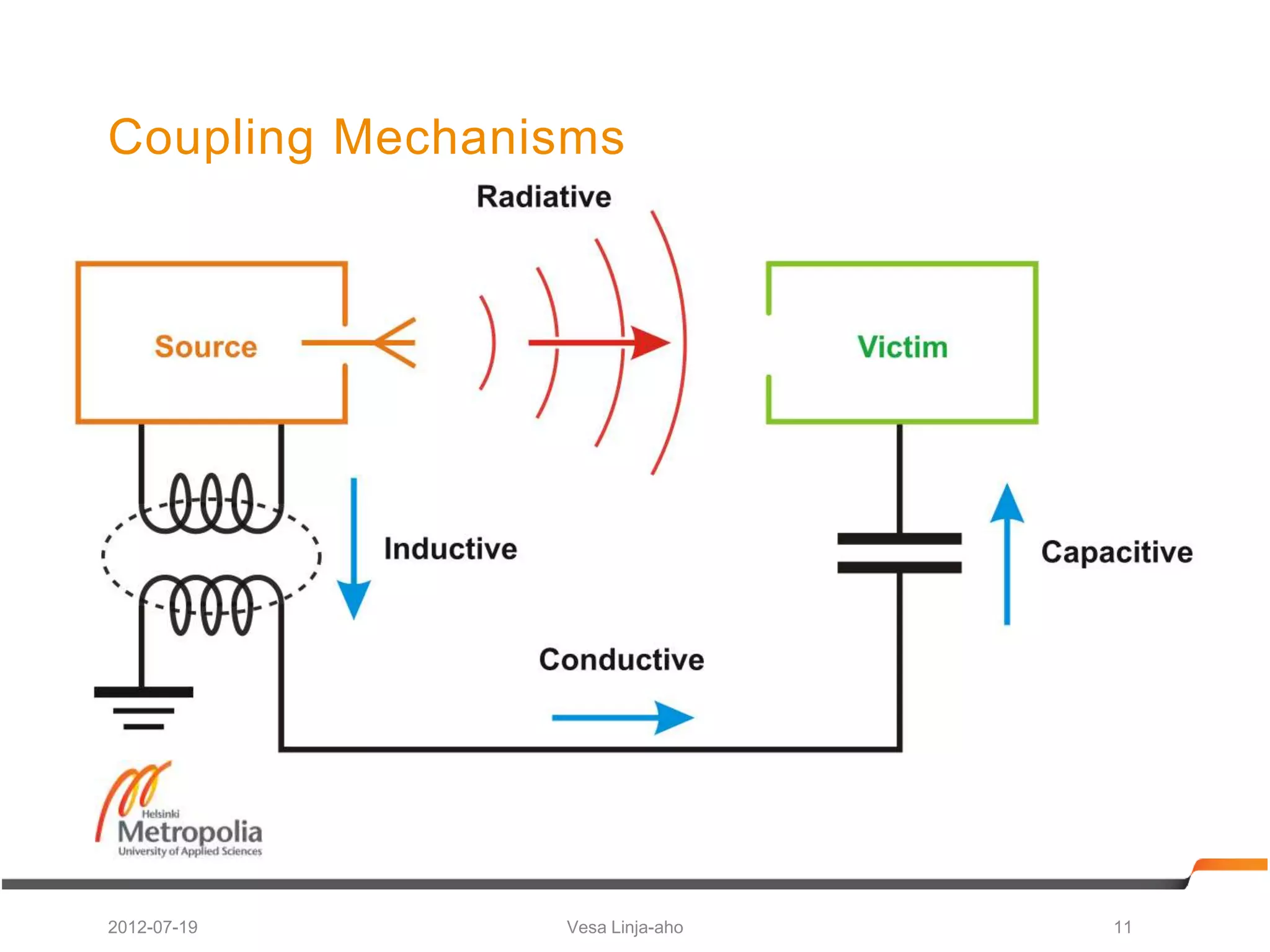


Vesa Linja-aho presents information on electromagnetic compatibility (EMC). He discusses how all electric devices should operate without interfering with other devices or being susceptible to normal interference. He covers common sources of electromagnetic interference and techniques to prevent issues, such as proper layout design, filtering of interfaces, and shielding of components. Linja-aho emphasizes that EMC should be considered from the beginning of a design process, not as an afterthought.


