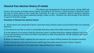
This document outlines topics related to semiconductor physics and optoelectronics physics, including:
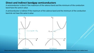
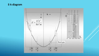
1. Free electron theory of metals, Bloch's theorem, energy band diagrams, direct and indirect bandgaps, density of states, and the types of electronic materials including metals, semiconductors and insulators.
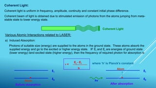
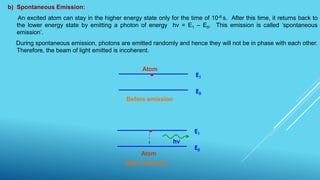
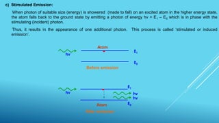
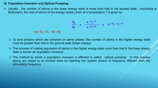
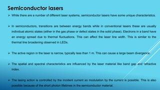
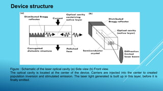
2. Lasers, which use stimulated emission of radiation to produce an intense, coherent beam of light. Key concepts covered include spontaneous emission, stimulated absorption, population inversion, and semiconductor lasers.
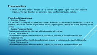
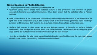
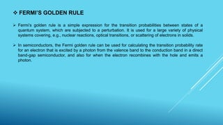
3. Photodetectors and noise sources, with reference made to the Fermi Golden Rule. The document provides an overview of key concepts that will be covered in more depth within these physics courses.
![Development of Free Electron Theory
The classical free electron theory [Drude and Lorentz]
It is a macroscopic theory, in which the electrons move freely in lattice and it obeys the laws of
classical mechanics. Here the electrons are assumed to move in a constant potential.
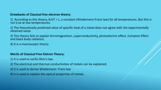
The quantum free electron theory [Sommerfeld Theory]
It is a microscopic theory, according to this theory the electrons in lattice moves in a constant
potential and it obeys law of quantum mechanics.
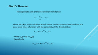
Brillouin Zone Theory [Band Theory]
Bloch developed this theory in which the electrons move in a periodic potential provided by
periodicity of crystal lattice. It explains the mechanisms of conductivity on the basis of energy bands
and hence band theory.
The electron theory explains the structure and properties of solids through their electronic structure.
It explains the binding in solids, behaviour of conductors and insulators, ferromagnetism, electrical and
thermal conductivities of solids, elasticity, cohesive and repulsive forces in solids etc.](https://image.slidesharecdn.com/ppt-physics-cse-ece1-240413050008-e4fd3ad3/85/PPT-Physics-CSE-ECE1pranil_arun_JADHAV_by-3-320.jpg)