Download to read offline
![Chapter 7
Electrically Symmetric
Poly(Phenylene Acetylene)
Diodes
Journal Molecular Crystals and Liquid Crystals (1994)
Vol. 256, pp. 555{561.
S. A. Jeglinski, M. E. Hollier, J. F. Gold, and Z. V. Vardeny
University of Utah, Physics Department, Salt Lake City, UT 84112
Y. Ding and T. Barton
Iowa State University, Chemistry Department, Ames, IA 50011
Abstract
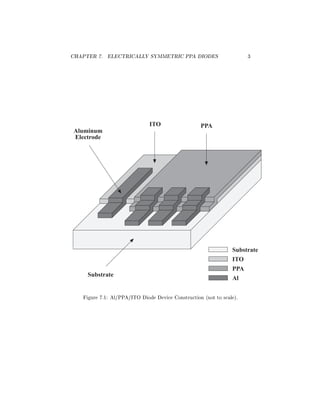
A diode has been fabricated with poly(phenylene acetylene) [PPA] as the elec-
troluminescent polymer. The device exhibited an unusual symmetric (positive
and negative bias) I{V characteristic and electroluminescent output. These ex-
perimental results are discussed in terms of tunneling of electrons and holes via
localized states.
Introduction
Luminescent conjugated polymers have recently attracted considerable interest
because of their use as active materials in light-emitting devices (LEDs) [1].
Operation as such depends upon the ability to inject into the polymer electrons
and holes, which then recombine to emit light.
1](https://image.slidesharecdn.com/diodes-100210095812-phpapp02/85/Electrically-Symmetric-Poly-Phenylene-Acetylene-Diodes-1-320.jpg)
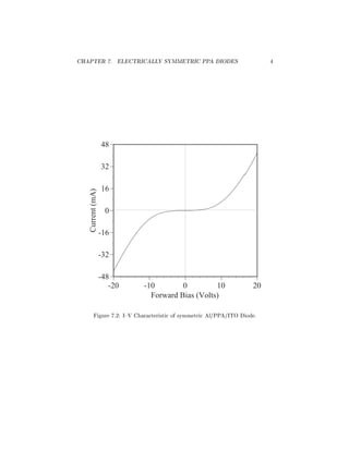
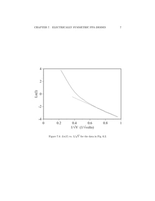

This document reports on the fabrication and testing of a luminescent diode utilizing poly(phenylene acetylene) (PPA), which displayed a symmetric current-voltage (I-V) characteristic and luminescence in both forward and reverse biases. The results suggest that tunneling via localized states accounts for the observed behavior at low voltages, while at higher voltages, non-ideal metal/polymer interface properties may allow similar barrier injection from either contact. The authors highlight the need for further research to explore these findings and their implications on the device's electrical characteristics.


![5G Explained! A High Level Overview [Introduction]](https://cdn.slidesharecdn.com/ss_thumbnails/5gexplainedahighleveloverview-260119165306-cc137a3e-thumbnail.jpg?width=640&height=640&fit=bounds)


