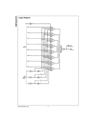
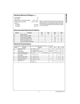
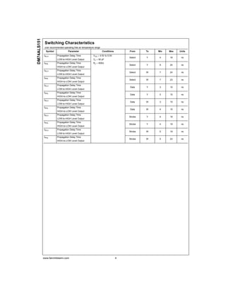
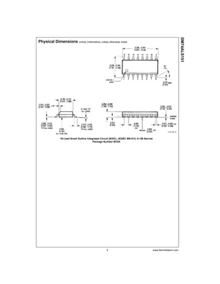
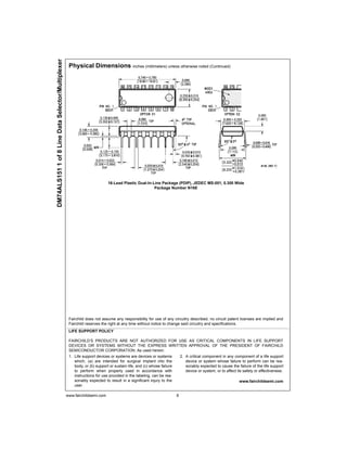
© 2000 Fairchild Semiconductor Corporation DS006203 www.fairchildsemi.com
April 1984
Revised February 2000
DM74ALS151
1
of
8
Line
Data
Selector/Multiplexer
DM74ALS151
1 of 8 Line Data Selector/Multiplexer
General Description
This Data Selector/Multiplexer contains full on-chip decod-
ing to select one-of-eight data sources as a result of a
unique three-bit binary code at the Select inputs. Two com-
plementary outputs provide both inverting and non-invert-
ing buffer operation. A Strobe input is provided which,
when at the high level, disables all data inputs and forces
the Y output to the LOW state and the W output to the
HIGH state. The Select input buffers incorporate internal
overlap features to ensure that select input changes do not
cause invalid output transients.
Features
■ Advanced oxide-isolated, ion-implanted Schottky TTL
process
■ Switching performance is guaranteed over full tempera-
ture and VCC supply range
■ Pin and functional compatible with LS family counterpart
■ Improved output transient handling capability
Ordering Code:
Devices also available in Tape and Reel. Specify by appending the suffix letter “X” to the ordering code.
Connection Diagram Function Table
H = HIGH Level
L = LOW Level
X = Don't Care
D0 thru D7 = the level of the respective D input
Order Number Package Number Package Description
DM74ALS151M M16A 16-Lead Small Outline Integrated Circuit (SOIC), JEDEC MS-012, 0.150 Narrow
DM74ALS151N N16E 16-Lead Plastic Dual-In-Line Package (PDIP), JEDEC MS-001, 0.300 Wide
Inputs Outputs
Select Strobe
Y W
C B A S
X X X H L H
L L L L D0 D0
L L H L D1 D1
L H L L D2 D2
L H H L D3 D3
H L L L D4 D4
H L H L D5 D5
H H L L D6 D6
H H H L D7 D7
www.fairchildsemi.com 2
DM74ALS151
Logic Diagram
3 www.fairchildsemi.com
DM74ALS151
Absolute Maximum Ratings(Note 1)
Note 1: The “Absolute Maximum Ratings” are those values beyond which
the safety of the device cannot be guaranteed. The device should not be
operated at these limits. The parametric values defined in the Electrical
Characteristics tables are not guaranteed at the absolute maximum ratings.
The “Recommended Operating Conditions” table will define the conditions
for actual device operation.
Recommended Operating Conditions
Electrical Characteristics
over recommended operating free-air temperature range. All typical values are measured at VCC = 5V, TA = 25°C.
Supply Voltage 7V
Input Voltage 7V
Operating Free Air Temperature Range 0°C to +70°C
Storage Temperature Range −65°C to +150°C
Typical θJA
N Package 78.0°C/W
M Package 107.0°C/W
Symbol Parameter Min Nom Max Units
VCC Supply Voltage 4.5 5 5.5 V
VIH HIGH Level Input Voltage 2 V
VIL LOW Level Input Voltage 0.8 V
IOH HIGH Level Output Current −2.6 mA
IOL LOW Level Output Current 24 mA
TA Free Air Operating Temperature 0 70 °C
Symbol Parameter Conditions Min Typ Max Units
VIK Input Clamp Voltage VCC = 4.5V, IIN = −18 mA −1.5 V
VOH HIGH Level VCC = 4.5V, IOH = Max 2.4 3.2 V
Output Voltage IOH = −400 µA, VCC = 4.5V to 5.5V VCC − 2 V
VOL LOW Level Output Voltage VCC = 4.5V IOL = 24 mA 0.35 0.5 V
II Input Current at Maximum
VCC = 5.5V, VIN = 7V 0.1 mA
Input Voltage
IIH HIGH Level Input Current VCC = 5.5V, VIN = 2.7V 20 µA
IIL LOW Level Input Current VCC = 5.5V, VIN = 0.4V −0.1 mA
IO Output Drive Current VCC = 5.5V, VOUT = 2.25V −30 −112 mA
ICC Supply Current VCC = 5.5V
7.5 12 mA
All Inputs = 4.5V
www.fairchildsemi.com 4
DM74ALS151
Switching Characteristics
over recommended operating free air temperature range
Symbol Parameter Conditions From To Min Max Units
tPLH Propagation Delay Time VCC = 4.5V to 5.5V
Select Y 4 18 ns
LOW-to-HIGH Level Output CL = 50 pF
tPHL Propagation Delay Time RL = 500Ω
Select Y 8 24 ns
HIGH-to-LOW Level Output
tPLH Propagation Delay Time
Select W 7 24 ns
LOW-to-HIGH Level Output
tPHL Propagation Delay Time
Select W 7 23 ns
HIGH-to-LOW Level Output
tPLH Propagation Delay Time
Data Y 3 10 ns
LOW-to-HIGH Level Output
tPHL Propagation Delay Time
Data Y 5 15 ns
HIGH-to-LOW Level Output
tPLH Propagation Delay Time
Data W 3 15 ns
LOW-to-HIGH Level Output
tPHL Propagation Delay Time
Data W 4 15 ns
HIGH-to-LOW Level Output
tPLH Propagation Delay Time
Strobe Y 4 18 ns
LOW-to-HIGH Level Output
tPHL Propagation Delay Time
Strobe Y 4 19 ns
HIGH-to-LOW Level Output
tPLH Propagation Delay Time
Strobe W 5 19 ns
LOW-to-HIGH Level Output
tPHL Propagation Delay Time
Strobe W 5 23 ns
HIGH-to-LOW Level Output
5 www.fairchildsemi.com
DM74ALS151
Physical Dimensions inches (millimeters) unless otherwise noted
16-Lead Small Outline Integrated Circuit (SOIC), JEDEC MS-012, 0.150 Narrow
Package Number M16A
www.fairchildsemi.com 6
DM74ALS151
1
of
8
Line
Data
Selector/Multiplexer
Physical Dimensions inches (millimeters) unless otherwise noted (Continued)
16-Lead Plastic Dual-In-Line Package (PDIP), JEDEC MS-001, 0.300 Wide
Package Number N16E
Fairchild does not assume any responsibility for use of any circuitry described, no circuit patent licenses are implied and
Fairchild reserves the right at any time without notice to change said circuitry and specifications.
LIFE SUPPORT POLICY
FAIRCHILD’S PRODUCTS ARE NOT AUTHORIZED FOR USE AS CRITICAL COMPONENTS IN LIFE SUPPORT
DEVICES OR SYSTEMS WITHOUT THE EXPRESS WRITTEN APPROVAL OF THE PRESIDENT OF FAIRCHILD
SEMICONDUCTOR CORPORATION. As used herein:
1. Life support devices or systems are devices or systems
which, (a) are intended for surgical implant into the
body, or (b) support or sustain life, and (c) whose failure
to perform when properly used in accordance with
instructions for use provided in the labeling, can be rea-
sonably expected to result in a significant injury to the
user.
2. A critical component in any component of a life support
device or system whose failure to perform can be rea-
sonably expected to cause the failure of the life support
device or system, or to affect its safety or effectiveness.
www.fairchildsemi.com

Data sheet of Integrated circuit DM74ALS151

  • 1.
    © 2000 FairchildSemiconductor Corporation DS006203 www.fairchildsemi.com April 1984 Revised February 2000 DM74ALS151 1 of 8 Line Data Selector/Multiplexer DM74ALS151 1 of 8 Line Data Selector/Multiplexer General Description This Data Selector/Multiplexer contains full on-chip decod- ing to select one-of-eight data sources as a result of a unique three-bit binary code at the Select inputs. Two com- plementary outputs provide both inverting and non-invert- ing buffer operation. A Strobe input is provided which, when at the high level, disables all data inputs and forces the Y output to the LOW state and the W output to the HIGH state. The Select input buffers incorporate internal overlap features to ensure that select input changes do not cause invalid output transients. Features ■ Advanced oxide-isolated, ion-implanted Schottky TTL process ■ Switching performance is guaranteed over full tempera- ture and VCC supply range ■ Pin and functional compatible with LS family counterpart ■ Improved output transient handling capability Ordering Code: Devices also available in Tape and Reel. Specify by appending the suffix letter “X” to the ordering code. Connection Diagram Function Table H = HIGH Level L = LOW Level X = Don't Care D0 thru D7 = the level of the respective D input Order Number Package Number Package Description DM74ALS151M M16A 16-Lead Small Outline Integrated Circuit (SOIC), JEDEC MS-012, 0.150 Narrow DM74ALS151N N16E 16-Lead Plastic Dual-In-Line Package (PDIP), JEDEC MS-001, 0.300 Wide Inputs Outputs Select Strobe Y W C B A S X X X H L H L L L L D0 D0 L L H L D1 D1 L H L L D2 D2 L H H L D3 D3 H L L L D4 D4 H L H L D5 D5 H H L L D6 D6 H H H L D7 D7
  • 2.
  • 3.
    3 www.fairchildsemi.com DM74ALS151 Absolute MaximumRatings(Note 1) Note 1: The “Absolute Maximum Ratings” are those values beyond which the safety of the device cannot be guaranteed. The device should not be operated at these limits. The parametric values defined in the Electrical Characteristics tables are not guaranteed at the absolute maximum ratings. The “Recommended Operating Conditions” table will define the conditions for actual device operation. Recommended Operating Conditions Electrical Characteristics over recommended operating free-air temperature range. All typical values are measured at VCC = 5V, TA = 25°C. Supply Voltage 7V Input Voltage 7V Operating Free Air Temperature Range 0°C to +70°C Storage Temperature Range −65°C to +150°C Typical θJA N Package 78.0°C/W M Package 107.0°C/W Symbol Parameter Min Nom Max Units VCC Supply Voltage 4.5 5 5.5 V VIH HIGH Level Input Voltage 2 V VIL LOW Level Input Voltage 0.8 V IOH HIGH Level Output Current −2.6 mA IOL LOW Level Output Current 24 mA TA Free Air Operating Temperature 0 70 °C Symbol Parameter Conditions Min Typ Max Units VIK Input Clamp Voltage VCC = 4.5V, IIN = −18 mA −1.5 V VOH HIGH Level VCC = 4.5V, IOH = Max 2.4 3.2 V Output Voltage IOH = −400 µA, VCC = 4.5V to 5.5V VCC − 2 V VOL LOW Level Output Voltage VCC = 4.5V IOL = 24 mA 0.35 0.5 V II Input Current at Maximum VCC = 5.5V, VIN = 7V 0.1 mA Input Voltage IIH HIGH Level Input Current VCC = 5.5V, VIN = 2.7V 20 µA IIL LOW Level Input Current VCC = 5.5V, VIN = 0.4V −0.1 mA IO Output Drive Current VCC = 5.5V, VOUT = 2.25V −30 −112 mA ICC Supply Current VCC = 5.5V 7.5 12 mA All Inputs = 4.5V
  • 4.
    www.fairchildsemi.com 4 DM74ALS151 Switching Characteristics overrecommended operating free air temperature range Symbol Parameter Conditions From To Min Max Units tPLH Propagation Delay Time VCC = 4.5V to 5.5V Select Y 4 18 ns LOW-to-HIGH Level Output CL = 50 pF tPHL Propagation Delay Time RL = 500Ω Select Y 8 24 ns HIGH-to-LOW Level Output tPLH Propagation Delay Time Select W 7 24 ns LOW-to-HIGH Level Output tPHL Propagation Delay Time Select W 7 23 ns HIGH-to-LOW Level Output tPLH Propagation Delay Time Data Y 3 10 ns LOW-to-HIGH Level Output tPHL Propagation Delay Time Data Y 5 15 ns HIGH-to-LOW Level Output tPLH Propagation Delay Time Data W 3 15 ns LOW-to-HIGH Level Output tPHL Propagation Delay Time Data W 4 15 ns HIGH-to-LOW Level Output tPLH Propagation Delay Time Strobe Y 4 18 ns LOW-to-HIGH Level Output tPHL Propagation Delay Time Strobe Y 4 19 ns HIGH-to-LOW Level Output tPLH Propagation Delay Time Strobe W 5 19 ns LOW-to-HIGH Level Output tPHL Propagation Delay Time Strobe W 5 23 ns HIGH-to-LOW Level Output
  • 5.
    5 www.fairchildsemi.com DM74ALS151 Physical Dimensionsinches (millimeters) unless otherwise noted 16-Lead Small Outline Integrated Circuit (SOIC), JEDEC MS-012, 0.150 Narrow Package Number M16A
  • 6.
    www.fairchildsemi.com 6 DM74ALS151 1 of 8 Line Data Selector/Multiplexer Physical Dimensionsinches (millimeters) unless otherwise noted (Continued) 16-Lead Plastic Dual-In-Line Package (PDIP), JEDEC MS-001, 0.300 Wide Package Number N16E Fairchild does not assume any responsibility for use of any circuitry described, no circuit patent licenses are implied and Fairchild reserves the right at any time without notice to change said circuitry and specifications. LIFE SUPPORT POLICY FAIRCHILD’S PRODUCTS ARE NOT AUTHORIZED FOR USE AS CRITICAL COMPONENTS IN LIFE SUPPORT DEVICES OR SYSTEMS WITHOUT THE EXPRESS WRITTEN APPROVAL OF THE PRESIDENT OF FAIRCHILD SEMICONDUCTOR CORPORATION. As used herein: 1. Life support devices or systems are devices or systems which, (a) are intended for surgical implant into the body, or (b) support or sustain life, and (c) whose failure to perform when properly used in accordance with instructions for use provided in the labeling, can be rea- sonably expected to result in a significant injury to the user. 2. A critical component in any component of a life support device or system whose failure to perform can be rea- sonably expected to cause the failure of the life support device or system, or to affect its safety or effectiveness. www.fairchildsemi.com