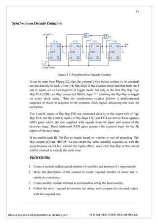
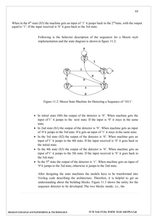
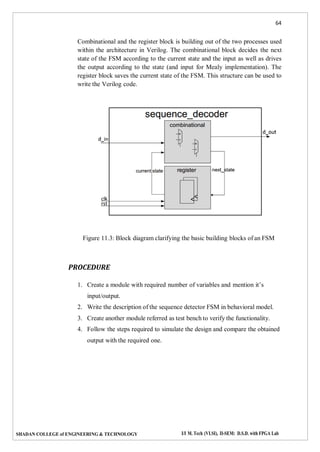
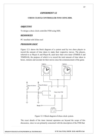
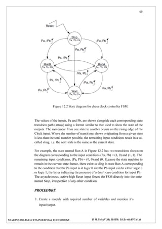
The document outlines the curriculum and objectives for a digital systems design course with a focus on FPGA lab applications at Shadan College of Engineering & Technology. It emphasizes the mission and vision of the institution, aiming to produce skilled engineers in electronics and communication through innovative teaching and research. The course aims to impart practical skills in Verilog HDL for designing, simulating, and testing digital circuit designs, along with broad outcomes applicable to industry standards and engineering principles.


![13
SHADAN COLLEGE of ENGINEERING & TECHNOLOGY I/I M. Tech (VLSI), II-SEM: D.S.D. with FPGA Lab
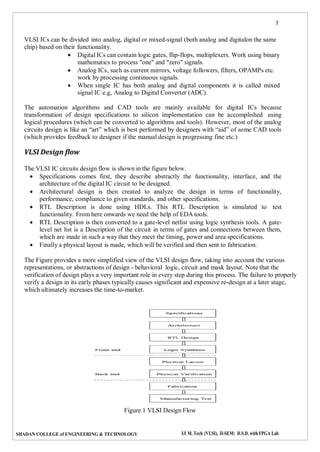
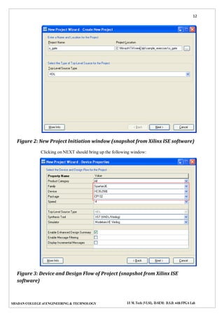
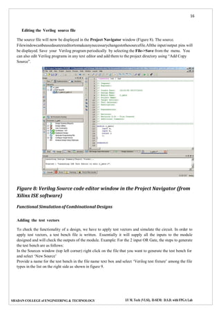
For each of the properties given below, click on the ‘value’ area and select from thelist of values
that appear.
Device Family: Family of the FPGA/CPLD used. In this laboratory we will be
using the Spartan3EFPGA’s.
Device: The number of the actual device. For this lab you may enter XC3S250E
(this can be found on the attached prototyping board)
Package: The type of package with the number of pins. The Spartan FPGA used in
this lab is packaged in CP132package.
Speed Grade: The Speed grade is“-4”.
Synthesis Tool: XST[VHDL/Verilog]
Simulator: The tool used to simulate and verify the functionality of the design.
Modelsim simulator is integrated in the Xilinx ISE. Hence choose “Modelsim-XE
Verilog” as the simulator or even Xilinx ISE Simulator can be used.
Then click on NEXT to save the entries.
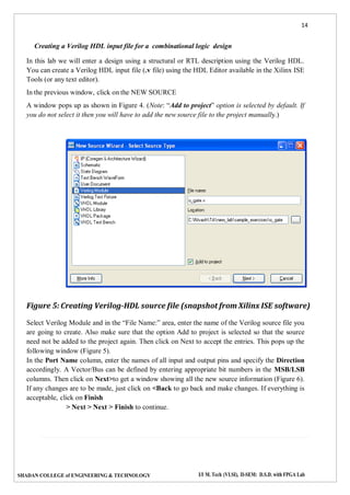
All project files such as schematics, netlists, Verilog files, VHDL files, etc., will be stored in a
subdirectory with the project name. A project can only have one top level HDL source file (or
schematic). Modules can be added to the project to create a modular, hierarchical design.
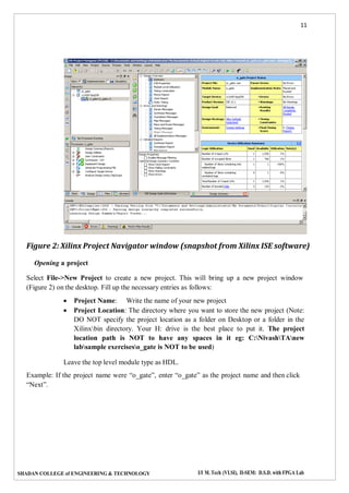
In order to open an existing project in Xilinx Tools, select File->Open Project to show the list
of projects on the machine. Choose the project you want and click OK.
Clicking on NEXT on the above window brings up the following window:
Figure 4: Create new source window (snapshot from Xilinx ISE software)
If creating a new source file, click on the NEW SOURCE.](https://image.slidesharecdn.com/digitalsystemdesignwithfpgaslabmanual-230421050916-cbc16f68/85/Digital-System-Design-with-FPGAs-Lab-Manual-pdf-13-320.jpg)

![23
SHADAN COLLEGE of ENGINEERING & TECHNOLOGY I/I M. Tech (VLSI), II-SEM: D.S.D. with FPGA Lab
performs a logical operation on one or more logical inputs, and produces a single logical output.
Depending on the context, the term may refer to an ideal logic gate, one that has for instance zero
rise time and unlimited fan-out, or it may refer to a non-ideal physical device.
VERILOGSOURCE CODE:
DATA FLOW MODEL:
modulelogicgates1(a,b,c);
input a;
input b;
output
[6:0]c;
assignc[0]=a&b;
assignc[1]=a|b;
assignc[2]=
~(a&b);assign c[3]=
~(a|b);
assignc[4]=a^ b;
assignc[5]= ~(a ^
b);assign c[6]=~ a;
endmodule
(OR)
module all(a,b,an,o,na,no,nt,xo,xn);
input a,b;
output (an,na,no,nt,xo,xn);
assign#5 an=a&b;
assign#5 na=~(a&b);
assign#5 o=a|b;
assign#5 no=~(a|b);
assign#5 nt=~a;
assign#5 xo=a^b;
assign#5 xn=~(a^b);
endmodule
BEHAVIOURAL MODELLING OF AND GATE:
module andg(a,b,an);
input a,b;
output an;
reg an;
always @(a or b)
begin
if(a==1`b0 && b==1`b0)
an=1`b0;
else if(a==1`b0 && b==1`b1)
an=1`b0;
else if(a==1`b1 && b=1`b0)
an=1`b0;
else if(a==1`b1 && b==1`b1)
an=1`b1;
end
endmodule](https://image.slidesharecdn.com/digitalsystemdesignwithfpgaslabmanual-230421050916-cbc16f68/85/Digital-System-Design-with-FPGAs-Lab-Manual-pdf-23-320.jpg)
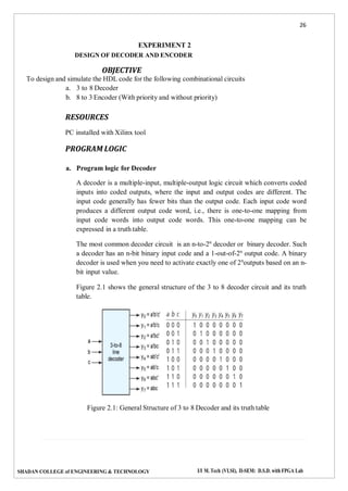
![28
SHADAN COLLEGE of ENGINEERING & TECHNOLOGY I/I M. Tech (VLSI), II-SEM: D.S.D. with FPGA Lab
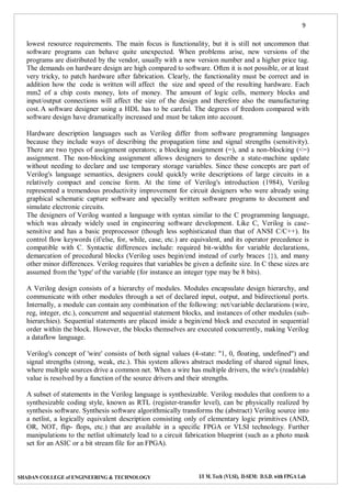
Figure 2.2: General Structure of 3 to 8 Decoder and its truth table
Decoder or encoder can be designed using HDL through its truth table in two ways: one is
using gate level modeling and another is by behavioral model.
PROCEDURE
1. Create a module with required number of variables and mention it’s input/output.
2. Implement the logic for decoder or encoder using behavioral or gate level model.
3. Create another module referred as test bench to verify the functionality.
4. Follow the steps required to simulate the design and compare the obtained output
with the corresponding truth table.
CODE
// 8 to 3 Encoder without priority
module p2(d,e);
input [7:0] d;
output [2:0]e;
assign e[2]= d[4] | d[5] | d[6] | d[7];
assign e[1]= d[2] | d[3] | d[6] | d[7];
assign e[0]= d[1] | d[3] | d[5] | d[7];
endmodule
// 8 to 3 Encoder with priority
module p4(din, dout);
input [7:0] din;
output [2:0] dout;
reg [2:0] dout;
always @(din)
begin
if (din[7]==1'b1) dout=3'b111;](https://image.slidesharecdn.com/digitalsystemdesignwithfpgaslabmanual-230421050916-cbc16f68/85/Digital-System-Design-with-FPGAs-Lab-Manual-pdf-28-320.jpg)
![29
SHADAN COLLEGE of ENGINEERING & TECHNOLOGY I/I M. Tech (VLSI), II-SEM: D.S.D. with FPGA Lab
else if (din[6]==1'b1) dout=3'b110;
else if (din[5]==1'b1) dout=3'b101;
else if (din[4]==1'b1) dout=3'b100;
else if (din[3]==1'b1) dout=3'b011;
else if (din[2]==1'b1) dout=3'b010;
else if (din[1]==1'b1) dout=3'b001;
else if (din[0]==1'b1) dout=3'b000;
else dout=3'bXXX;
end
endmodule
// 3 to 8 decoder
module p3(i,d);
input [2:0]i;
output [7:0]d;
assign d[0]=(~i[2])&(~i[1])&(~i[0]);
assign d[1]=(~i[2])&(~i[1])&(i[0]);
assign d[2]=(~i[2])&(i[1])&(~i[0]);
assign d[3]=(~i[2])&(i[1])&(i[0]);
assign d[4]=(i[2])&(~i[1])&(~i[0]);
assign d[5]=(i[2])&(~i[1])&(i[0]);
assign d[6]=(i[2])&(i[1])&(~i[0]);
assign d[7]=(i[2])&(i[1])&(i[0]);
endmodule
PRE LAB QUESTIONS
1. What is a decoder?
2. What for enable inputs are used in decoder?
3. What are the applications of decoder?
4. What is an encoder?
5. What is a priority encoder?
6. How many input and output lines are there for a 128x7 encoder.
LAB ASSIGNMENT
1. Implement full adder circuit using decoder and two OR gates.
2. Implement 3x8 decoder using 2x4 decoder and additional logic.
3. Construct a 4x16 decoder using two 3x8 decoder and additional logic. Show the
schematic diagram neatly?
4. Design 2-to-4 decoder using only NOR gates.
5. Construct a 5 x 32 decoder with four 3x 8 decoders with enable and one 2 x 4
decoder.
6. Write a Verilog code to implement Octal-to-Binary Encoder?](https://image.slidesharecdn.com/digitalsystemdesignwithfpgaslabmanual-230421050916-cbc16f68/85/Digital-System-Design-with-FPGAs-Lab-Manual-pdf-29-320.jpg)

![33
SHADAN COLLEGE of ENGINEERING & TECHNOLOGY I/I M. Tech (VLSI), II-SEM: D.S.D. with FPGA Lab
PROCEDURE
1. Create a module with required number of variables and mention it’s input/output.
2. Write the description of the multiplexer or demultiplexer using data flow model
or gate level model
3. Create another module referred as test bench to verify the functionality.
4. Follow the steps required to simulate the design and compare the obtained output
with the corresponding truth table.
CODE
// 8:1 multiplexer
module p5(s,i,y);
input [7:0]i;
input [2:0]s;
output y;
wire [2:0]sb;
not(sb[0],s[0]);
not(sb[1],s[1]);
not(sb[2],s[2]);
assign y = (sb[2]&sb[1]&sb[0]&i[0]) | (sb[2]&sb[1]&s[0]&i[1]) |
(sb[2]&s[1]&sb[0]&i[2]) | (sb[2]&s[1]&s[0]&i[3]) | (s[2]&sb[1]&sb[0]&i[4]) |
(s[2]&sb[1]&s[0]&i[5]) | (s[2]&s[1]&sb[0]&i[6]) | (s[2]&s[1]&s[0]&i[7]);
endmodule
//1:8 Demultiplexer
module p6(din,s,dout);
output [7:0]dout ;
input din ;
input [2:0]s ;
assign dout[7] = din & (s[2]) & (s[1]) & (s[0]);
assign dout[6] = din & (s[2]) & (s[1]) & (~s[0]);
assign dout[5] = din & (s[2]) & (~s[1]) & (s[0]);
assign dout[4] = din & (s[2]) & (~s[1]) & (~s[0]);
assign dout[3] = din & (~s[2]) & (s[1]) & (s[0]);
assign dout[2] = din & (~s[2]) & (s[1]) & (~s[0]);
assign dout[1] = din & (~s[2]) & (~s[1]) & (s[0]);
assign dout[0] = din & (~s[2]) & (~s[1]) & (~s[0]);
endmodule
PRE LAB QUESTIONS
1. What is a multiplexer?
2. What is the relationship between input lines and select lines?](https://image.slidesharecdn.com/digitalsystemdesignwithfpgaslabmanual-230421050916-cbc16f68/85/Digital-System-Design-with-FPGAs-Lab-Manual-pdf-33-320.jpg)
![36
SHADAN COLLEGE of ENGINEERING & TECHNOLOGY I/I M. Tech (VLSI), II-SEM: D.S.D. with FPGA Lab
b. To obtain the successive second binary bit, perform the EX-OR operation
between the first bit or most significant digit of binary to the second bit of the
given grey code.
c. To obtain the successive third binary bit, perform the EX-OR operation between
the second bit or most significant digit of binary to the third MSD (most
significant digit) of grey code and so on for the next successive binary bits
conversion to find the equivalent.
PROCEDURE
1. Create a module with required number of variables and mention it’s input/output.
2. Write the description of the code converter using data flow model or gate level
model.
3. Create another module referred as test bench to verify the functionality.
4. Follow the steps required to simulate the design and compare the obtained output
with the required one.
CODE
// binary to gray code converter
module p7(b,g);
input [3:0] b;
output [3:0] g;
reg [3:0] g;
always@(b)
begin
g[3]=b[3];
g[2]=b[3]^b[2];
g[1]=b[2]^b[1];
g[0]=b[1]^b[0];
end
endmodule
//gray to binary converter
module p8(g,b);
input [3:0] g;
output [3:0] b;
reg [3:0] b;
always@(g)
begin
b[3]=g[3];](https://image.slidesharecdn.com/digitalsystemdesignwithfpgaslabmanual-230421050916-cbc16f68/85/Digital-System-Design-with-FPGAs-Lab-Manual-pdf-36-320.jpg)
![37
SHADAN COLLEGE of ENGINEERING & TECHNOLOGY I/I M. Tech (VLSI), II-SEM: D.S.D. with FPGA Lab
b[2]=b[3]^g[2];
b[1]=b[2]^g[1];
b[0]=b[1]^g[0];
end
endmodule
// 4 bit comparator
module p9(a,b,g,l,e);
input [3:0]a;
input [3:0]b;
output g,l,e;
reg g,l,e;
always@(a,b)
begin
if (a<b)
begin
e = 0; l = 1; g = 0;
end
else if (a==b)
begin
e = 1; l = 0; g = 0;
end
else
begin
e = 0; l = 0; g = 1;
end
end
endmodule
PRE LAB QUESTIONS
1. What is a code converter? List some of the code converters.
2. What are the typical applications of gray code?
3. Distinguish between the weighted and non-weighted codes. Give examples.
4. Realize the Boolean expressions for binary to gray code conversion
5. Realize the Boolean expressions for gray to binary code conversion](https://image.slidesharecdn.com/digitalsystemdesignwithfpgaslabmanual-230421050916-cbc16f68/85/Digital-System-Design-with-FPGAs-Lab-Manual-pdf-37-320.jpg)
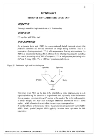
![43
SHADAN COLLEGE of ENGINEERING & TECHNOLOGY I/I M. Tech (VLSI), II-SEM: D.S.D. with FPGA Lab
Arithmetic operations
Bitwise logical operations
Bit shift operations
In this lab, students have to design an 8-bit ALU to implement the following
operations:
Table 1: ALU Instructions
Control Instruction Operation
000 Add Ouput<= A+B+Cin (Cout is carry)
001 Sub Output <= A-B-C (Cou is barrow)
010 Or Output <= A or B
011 And Output <= A and B
100 Shl Output <= A[7:0] & ‘0’
101 Shr Output <= ‘0’ & A[7:1]
110 Rol Output <= A[2:0] & A[7]
111 Ror Output <= A[0] & A[7:1]
Table 1 also illustrates the encoding of the control input
The 4 - bit ALU has the following inputs:
A: 8-bit input
B: 8-bit input
Cin: 1-bit input
Output: 8-bit output
Cout: 1-bit output
Control: 3-bit control input
The following points should be taken care of:
Use a case statement (or a similar ‘combinational’ statement) that checks the
input combination of “Code” and acts on A, B, and Cin as described in
Table1.
The above circuit is completely combinational. The output should change as
soon as the code combination or any of the input changes.
You can use arithmetic and logical operators to realize your design.
PROCEDURE
1. Create a module with required number of variables and mention it’s input/output.
2. Write the description of the ALU by using case statements.
3. Create another module referred as test bench to verify the functionality.
4. Follow the steps required to simulate the design and compare the obtained output
with the required one.](https://image.slidesharecdn.com/digitalsystemdesignwithfpgaslabmanual-230421050916-cbc16f68/85/Digital-System-Design-with-FPGAs-Lab-Manual-pdf-43-320.jpg)
![44
SHADAN COLLEGE of ENGINEERING & TECHNOLOGY I/I M. Tech (VLSI), II-SEM: D.S.D. with FPGA Lab
CODE
//8 bit ALU
module p13(z,a,b,sel);
input [7:0]a,b;
input [3:0]sel;
output [7:0]z;
reg [7:0]z;
always@(sel,a,b)
begin
case(sel)
4'b0000: z=a+b;
4'b0001: z=a-b;
4'b0010: z=b-1;
4'b0011: z=a*b;
4'b0100: z=a&&b;
4'b0101: z=a||b;
4'b0110: z=!a;
4'b0111: z=~a;
4'b1000: z=a&b;
4'b1001: z=a|b;
4'b1010: z=a^b;
4'b1011: z=a<<1;
4'b1100: z=a>>1;
4'b1101: z=a+1;
4'b1110: z=a-1;
endcase
end
endmodule
PRE LAB QUESTIONS
1. State the basic units of the computer. Name the subunits that make up the CPU,
and give the function of each of the units.
2. Give the description of computer architecture.
3. What are arithmetic operations
4. What are bitwise logical operations
5. What are bit shift operations
LAB ASSIGNMENT
1. Design the 4-bit ALU
2. Write a HDL code to implement basic arithmetic operations using ALU.
POST LAB QUESTIONS
1. Write a HDL code to implement bitwise logical operations using ALU.
2. Write a HDL code to implement bit shift operations using ALU.](https://image.slidesharecdn.com/digitalsystemdesignwithfpgaslabmanual-230421050916-cbc16f68/85/Digital-System-Design-with-FPGAs-Lab-Manual-pdf-44-320.jpg)
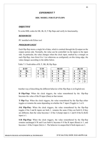
![46
SHADAN COLLEGE of ENGINEERING & TECHNOLOGY I/I M. Tech (VLSI), II-SEM: D.S.D. with FPGA Lab
PROCEDURE
1. Create a module with required number of variables and mention it’s input/output.
2. Write the description of the flip flops using behavioral model
3. Create another module referred as test bench to verify the functionality.
4. Follow the steps required to simulate the design and compare the obtained output
with the required one.
CODE
//SR flipflop
module p14(s,r,clk,q,qb);
input s,r,clk;
output q,qb;
reg q,qb;
reg [1:0]sr;
wire qp=1'b0;
always@(posedge clk)
begin sr={s,r};
begin
case (sr)
2'd0:q=qp;
2'd1:q=1'b0;
2'd2:q=1'b1;
2'd3:q=1'bX;
endcase
end
qb=~q;
end
endmodule
//JK flipflop
module p15(j,k,clk,q,qb);
input j,k,clk;
output q,qb;
reg q,qb;
reg [1:0]jk;
wire qp=1'b0;
always@(posedge clk)
begin jk={j,k};
begin
case (jk)
2'd0:q=qp;
2'd1:q=1'b0;
2'd2:q=1'b1;
2'd3:q=~q;
endcase](https://image.slidesharecdn.com/digitalsystemdesignwithfpgaslabmanual-230421050916-cbc16f68/85/Digital-System-Design-with-FPGAs-Lab-Manual-pdf-46-320.jpg)
![52
SHADAN COLLEGE of ENGINEERING & TECHNOLOGY I/I M. Tech (VLSI), II-SEM: D.S.D. with FPGA Lab
CODE
// binary counter
module p18(clk,count );
output [3:0] count ;
reg [3:0] count ;
input clk ;
wire clk ;
initial count = 0;
always @ (posedge (clk))
begin
count <= count + 1;
end
endmodule
//BCD counter
module p19(clk ,reset ,dout );
output [3:0] dout ;
reg [3:0] dout ;
input clk ;
wire clk ;
input reset ;
wire reset ;
initial dout = 0 ;
always @ (posedge (clk))
begin
if (reset) dout <= 0;
else if (dout<=9)
begin
dout <= dout + 1;
end
else if (dout==9)
begin
dout <= 0;
end
end
endmodule
PRE LAB QUESTIONS
1. How many number of flip-flops required in a decade counter?
2. How many number of flip-flops required in a Mod – N Counter?
3. What is the difference between synchronous and asynchronous counters?
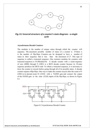
4. An n stage ripple counter can count up to .](https://image.slidesharecdn.com/digitalsystemdesignwithfpgaslabmanual-230421050916-cbc16f68/85/Digital-System-Design-with-FPGAs-Lab-Manual-pdf-52-320.jpg)
![56
SHADAN COLLEGE of ENGINEERING & TECHNOLOGY I/I M. Tech (VLSI), II-SEM: D.S.D. with FPGA Lab
CODE
//universal shift register
module p20(op,in,s,MSB_in,LSB_in,clk);
input [3:0]in;
input [1:0]s;
input MSB_in, LSB_in,clk;
output [3:0]op;
reg [3:0]op;
always @( posedge clk)
case (s)
2'b00: op <= op;
2'b01: op <= {MSB_in, op[3:1]};
2'b10: op <= {op[2:0], LSB_in};
2'b11: op <= in;
endcase
endmodule
PRE LAB QUESTIONS
1. What is a register
2. What is a shift register?
3. Mention the various shift operations.
4. What is the difference between logical shift and arithmetic shift?
LAB ASSIGNMENT
1. Design a shift right register.
2. Design a shift left register.
3. Design a circular shift right register using JK flip flop.
4. Design a circular left right register using JK flip flop.
POST LAB QUESTIONS
1. Write a HDL code to load the data parallel in universal shift register.
2. Write a HDL code to load the data serial in universal shift register.
3. Write a HDL code to perform serial in parallel out (SIPO) operation in universal
shift register.
4. Write a HDL code to perform serial in serial out (SISO) operation in universal
shift register.
5. Write a HDL code to perform parallel in serial out (PISO) operation in universal
shift register.
6. Write a HDL code to perform parallel in parallel out (SISO) operation in
universal shift register.](https://image.slidesharecdn.com/digitalsystemdesignwithfpgaslabmanual-230421050916-cbc16f68/85/Digital-System-Design-with-FPGAs-Lab-Manual-pdf-56-320.jpg)
![60
SHADAN COLLEGE of ENGINEERING & TECHNOLOGY I/I M. Tech (VLSI), II-SEM: D.S.D. with FPGA Lab
Figure 10.1 Carry-lookahead Adder
For simplicity, we are assuming that all gates have the same delay time. This
assumption may or may not be true depending on the target technology that is
being used to implement your logic. However, for the sake of comparison with
other addition techniques, this model works well. Summarizing the above steps,
we can see that the propagation delay for a 4-bit adder is no longer determined by
a carry chain and is only four gate-delays, (∆g= 4). The pre-lab assignment will
include an exercise which asks you to look at the gate count of a 4-bit Carry-
Lookahead Adder.
PROCEDURE
1. Create a module with required number of variables and mention it’s
input/output.
2. Write the description of the carry look ahead adder using data flow model or
gate level model.
3. Create another module referred as test bench to verify the functionality.
4. Follow the steps required to simulate the design and compare the obtained
output with the required one.
CODE
module p21(a,b,cin,sum,cout);
input[3:0] a,b;
input cin;](https://image.slidesharecdn.com/digitalsystemdesignwithfpgaslabmanual-230421050916-cbc16f68/85/Digital-System-Design-with-FPGAs-Lab-Manual-pdf-60-320.jpg)
![61
SHADAN COLLEGE of ENGINEERING & TECHNOLOGY I/I M. Tech (VLSI), II-SEM: D.S.D. with FPGA Lab
output [3:0] sum;
output cout;
wire p0,p1,p2,p3,g0,g1,g2,g3,c1,c2,c3,c4;
assign p0=(a[0]^b[0]),
p1=(a[1]^b[1]),
p2=(a[2]^b[2]),
p3=(a[3]^b[3]);
assign g0=(a[0]&b[0]),
g1=(a[1]&b[1]),
g2=(a[2]&b[2]),
g3=(a[3]&b[3]);
assign c0=cin,
c1=g0|(p0&cin),
c2=g1|(p1&g0)|(p1&p0&cin),
c3=g2|(p2&g1)|(p2&p1&g0)|(p1&p1&p0&cin),
c4=g3|(p3&g2)|(p3&p2&g1)|(p3&p2&p1&g0)|(p3&p2&p1&p0&cin);
assign sum[0]=p0^c0,
sum[1]=p1^c1,
sum[2]=p2^c2,
sum[3]=p3^c3;
assign cout=c4;
endmodule
PRE LAB QUESTIONS
1. What is the functionality of the adder?
2. Design a ripple carry adder and mention its disadvantage.
3. List the various adders and its pros and cons.
LAB ASSIGNMENT
1. Design 4-bit ripple carry adder using HDL.
2. Design 4-bit carry look ahead adder using HDL.
3. Observe the RTL schematic of the designed 4-bit look ahead adder.
POST LAB QUESTIONS
1. How many gates are required to design 4-bit look ahead adder.
2. How many lookup tables are required to implement the 4-bit look ahead
adder?
3. What is synthesis process?
4. Design 32-bit carry look ahead adder using HDL.](https://image.slidesharecdn.com/digitalsystemdesignwithfpgaslabmanual-230421050916-cbc16f68/85/Digital-System-Design-with-FPGAs-Lab-Manual-pdf-61-320.jpg)
![65
SHADAN COLLEGE of ENGINEERING & TECHNOLOGY I/I M. Tech (VLSI), II-SEM: D.S.D. with FPGA Lab
CODE
// sequence detector
module p22(clk, rst, inp, outp);
input clk, rst, inp;
output outp;
reg [1:0] state;reg outp;
always @( posedge clk, rst )
begin
if( rst )
state <= 2'b00;
else
begin
case( {state,inp} )
3'b000: begin
state <= 2'b00;
end
3'b001: begin
state <= 2'b01;
end
3'b010: begin
state <= 2'b10;
end
3'b011: begin
state <= 2'b01;
end
3'b100: begin
state <= 2'b10;
end
3'b101: begin
state <= 2'b11;
end
3'b110: begin
state <= 2'b10;
end
3'b111: begin
state <= 2'b01;
end
endcase
end
assign outp = (({state,inp})==3'b111)? 1'b1 : 1'b0;
end
endmodule
PRE LAB QUESTIONS
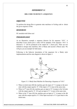
1. Design a FSM to detect the sequence ‘1010’.
2. Design a state flow diagram for the sequence detector FSM ‘10010’.
3. Design the state table for the sequence detector FSM ‘10010’.](https://image.slidesharecdn.com/digitalsystemdesignwithfpgaslabmanual-230421050916-cbc16f68/85/Digital-System-Design-with-FPGAs-Lab-Manual-pdf-65-320.jpg)

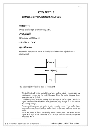
![70
SHADAN COLLEGE of ENGINEERING & TECHNOLOGY I/I M. Tech (VLSI), II-SEM: D.S.D. with FPGA Lab
2. Write the description of the chess clock controller FSM using behavioral
model.
3. Create another module referred as test bench to verify the functionality.
4. Follow the steps required to simulate the design and compare the obtained
output with the required one.
CODE
// chess clock timer
module p23(input reset,Pa,Pb,clock,output Ta,Tb,Clr);
localparam RunA = 0,RunB = 1,Stop = 2,Wait = 3;
reg[1:0]state;
always@(posedge clock or posedge reset)
begin
if(reset)
state<= Stop;
else
case(state)
RunA:
casex({Pa,Pb})
2'b0x:state<= RunA;
2'b10:state<= RunB;
endcase 2'b11:state<= Wait;
RunB:
casex({Pa,Pb})
2'bx0:state<= RunB;
2'b01:state<= RunA;
2'b11:state<= Wait;
endcase
Stop:
case({Pa,Pb})
2'b00:state<= Stop;
2'b01:state<= RunA;
2'b10:state<= RunB;
endcase
2'b11:state<= Wait;
Wait:if(Pa == Pb)
state<= Wait;
else if(Pa == 1'b1)
state<= RunB;
else
state<= RunA;
endcase
end
assign Ta = state == RunA;](https://image.slidesharecdn.com/digitalsystemdesignwithfpgaslabmanual-230421050916-cbc16f68/85/Digital-System-Design-with-FPGAs-Lab-Manual-pdf-70-320.jpg)
![74
SHADAN COLLEGE of ENGINEERING & TECHNOLOGY I/I M. Tech (VLSI), II-SEM: D.S.D. with FPGA Lab
reg g ;
input clk ;
wire clk ;
input sensor ;
wire sensor ;
parameter red = 0;
parameter yellow = 1;
parameter green = 2;
reg [1:0] p_state;
reg [1:0] n_state;
initial p_state = red;
always @ (posedge (clk)) begin
p_state <= n_state;
end
always @ (p_state or sensor) begin
case (p_state)
red : n_state = green ;
green : begin
if (sensor)
n_state = green;
else
n_state = yellow;
end
yellow : n_state = red ;
endcase
end
always @ (p_state) begin
case (p_state)
red : begin
r = 1;
y = 0;
g = 0;
end
yellow : begin
r = 0;
y = 1;
g = 0;
end
green : begin
if (sensor)
n_state = green;
else
n_state = yellow;
r = 0;
y = 0;
g = 1;
end](https://image.slidesharecdn.com/digitalsystemdesignwithfpgaslabmanual-230421050916-cbc16f68/85/Digital-System-Design-with-FPGAs-Lab-Manual-pdf-74-320.jpg)
![77
SHADAN COLLEGE of ENGINEERING & TECHNOLOGY I/I M. Tech (VLSI), II-SEM: D.S.D. with FPGA Lab
Third, define the Out_Current_Floor, Direction, Complete, Door_Alert and
Weight_Alert as reg then assign them equal to the output. Therefore, those
variables will run as a register and output.
Next, when the Reset is off the variable Complete, Door Alert and Weight Alert
will be initialized to be zero. Similarly, when the Request_Floor is on, the variable
In_Current_Floor is set to be equal to Out_Current_Floor only once.
Then, In_Current_Floor stay the same, Out_Current_Floor keep changing
(updating) and compare with request floor, until Out_Current_Floor is at the same
level as Request_Floor.
Lastly, define three cases of if statement for the elevator. There are cases for
normal running cases – (comparing between Request_Floor and
Out_Current_Floor to decide the moving direction), door open for more than three
minutes - (turn on the Door_Alert) and overweight cases for elevator - (turn on the
Weight_Alert).
While designing a lift controller number of states depends on number of
levels/floors. If you want to design a three floor lift then three states are required.
And one need design the finite state machine using those three states and have to
mention the function of the each state.
PROCEDURE
1. Create a module with required number of variables and mention it’s
input/output.
2. Write the description of the finite state machine using behavioral model.
3. Create another module referred as test bench to verify the functionality.
4. Follow the steps required to simulate the design and compare the obtained
output with the required one.
CODE
// Elevator
module p25(request_floor, in_current_floor, clk, reset, complete, direction,
out_current_floor);
input [2:0] request_floor;
input [2:0] in_current_floor;
input clk;
input reset; //1 bit input reset
output [2:0] out_current_floor;
output direction;
output complete;](https://image.slidesharecdn.com/digitalsystemdesignwithfpgaslabmanual-230421050916-cbc16f68/85/Digital-System-Design-with-FPGAs-Lab-Manual-pdf-77-320.jpg)
![78
SHADAN COLLEGE of ENGINEERING & TECHNOLOGY I/I M. Tech (VLSI), II-SEM: D.S.D. with FPGA Lab
reg r_direction;
reg r_complete;
reg [2:0] r_out_current_floor;
reg [6:0] clk_count;
reg clk_100;
reg clk_trigger;
assign direction = r_direction;
assign complete = r_complete;
assign out_current_floor = r_out_current_floor;
always @ (negedge reset)
begin
clk_100 = 1'b0;
clk_count = 0;
clk_trigger = 1'b0;
r_complete= 1'b0;
end
always @ (posedge clk)
begin
if (clk_trigger)
begin
clk_count = clk_count +1;
end
if (clk_count == 5000)
begin
clk_100 =~ clk_100;
clk_count = 0;
end
end
always @ (request_floor)
begin
clk_trigger =1 ;
clk_100 =~ clk_100;
r_out_current_floor <= in_current_floor;
end
always @ (posedge clk) begin
if (!reset)
begin
if (request_floor > r_out_current_floor)
begin
r_direction = 1'b1;
r_out_current_floor <= r_out_current_floor << 1;
end](https://image.slidesharecdn.com/digitalsystemdesignwithfpgaslabmanual-230421050916-cbc16f68/85/Digital-System-Design-with-FPGAs-Lab-Manual-pdf-78-320.jpg)