Download to read offline

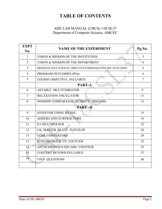
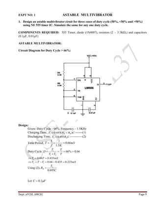
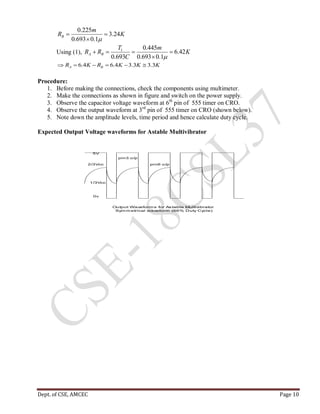


This document outlines the syllabus for the Analog and Digital Electronics Laboratory course for the third semester Computer Science students. It includes the vision, mission, objectives, and outcomes of both the institution and department. The syllabus covers both analog and digital circuits through 9 experiments involving components like timers, operational amplifiers, adders/subtractors, multiplexers, flip-flops, and counters. Students will design, simulate, implement, and test the circuits both in hardware and HDL. The goal is for students to apply design skills and gain practical experience with electronic components and tools.