Download to read offline

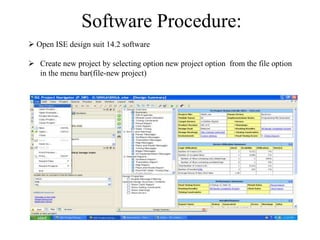
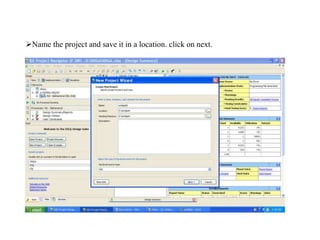
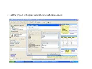
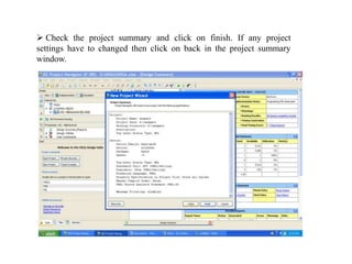
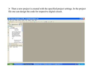

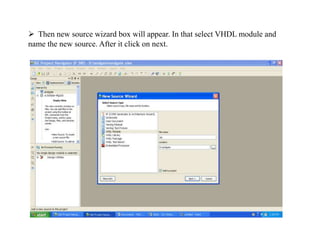
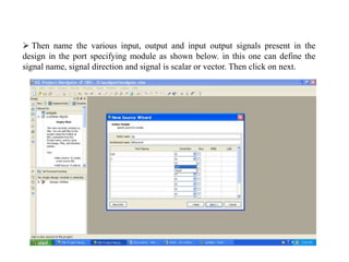
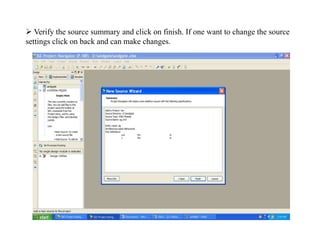
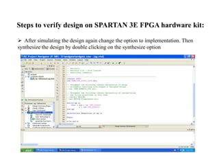
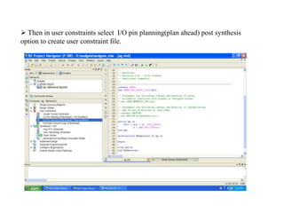
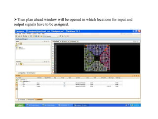
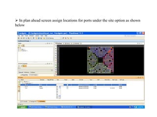
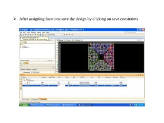
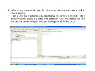
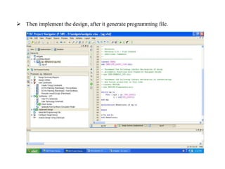
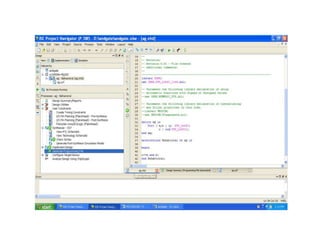
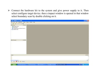


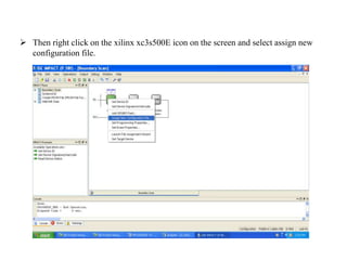

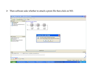
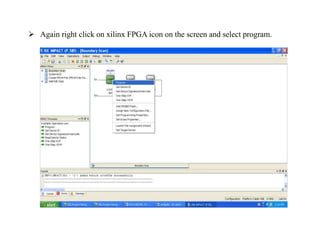
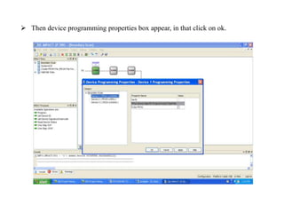
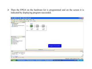


1. The document describes the steps to design and verify a digital circuit using Xilinx ISE Design Suite 12.1 software. 2. It involves creating a new project, designing the circuit code using VHDL, simulating the design, synthesizing it, assigning I/O pins, generating a programming file, and programming an FPGA board to verify the circuit operation. 3. Key steps are opening ISE software, making a new project, adding a VHDL module, assigning ports, implementing the design, generating a programming file, initializing and programming the FPGA board using the bit file, and testing the circuit.