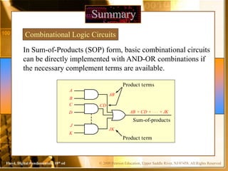
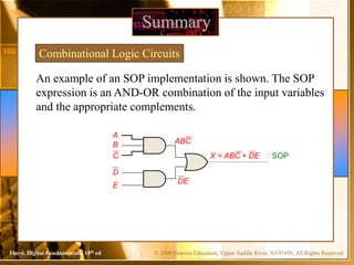
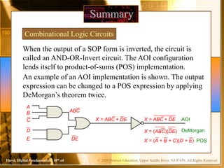
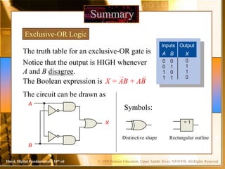
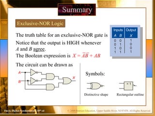
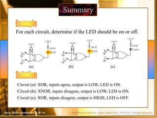
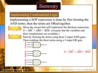
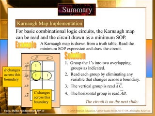
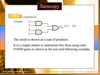
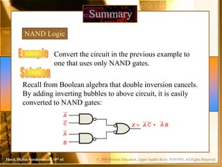
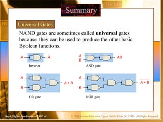
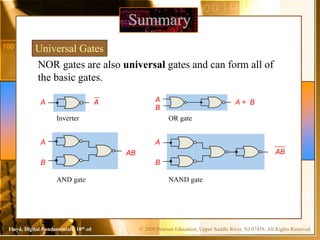
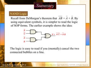
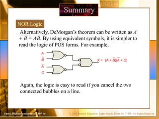
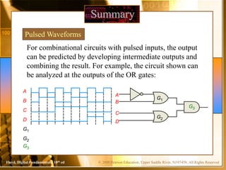
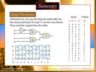
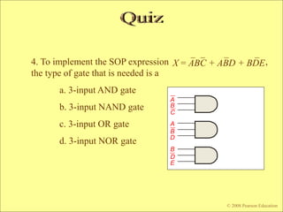
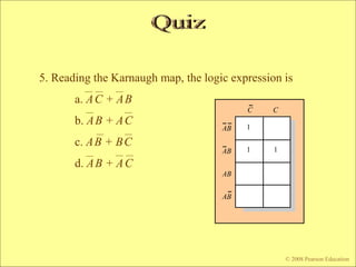
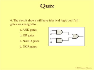
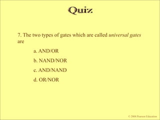
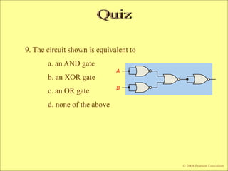
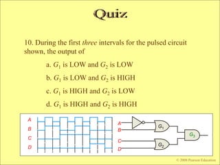
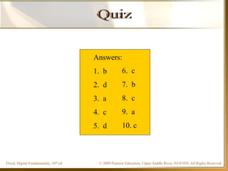
© 2009 Pearson Education, Upper Saddle River, NJ 07458. All Rights Reserved
Floyd, Digital Fundamentals, 10th ed
Digital
Fundamentals
Tenth Edition
Floyd
Chapter 5
© 2008 Pearson Education
© 2009 Pearson Education, Upper Saddle River, NJ 07458. All Rights Reserved
Floyd, Digital Fundamentals, 10th ed
In Sum-of-Products (SOP) form, basic combinational circuits
can be directly implemented with AND-OR combinations if
the necessary complement terms are available.
Summary
Combinational Logic Circuits
JK
J
K
A
B
AB
Product terms
Sum-of-products
Product term
C
D
CD
AB + CD + + JK
. . .
© 2009 Pearson Education, Upper Saddle River, NJ 07458. All Rights Reserved
Floyd, Digital Fundamentals, 10th ed
Summary
An example of an SOP implementation is shown. The SOP
expression is an AND-OR combination of the input variables
and the appropriate complements.
Combinational Logic Circuits
SOP
DE
ABC
A
B
C
E
D
X = ABC + DE
© 2009 Pearson Education, Upper Saddle River, NJ 07458. All Rights Reserved
Floyd, Digital Fundamentals, 10th ed
When the output of a SOP form is inverted, the circuit is
called an AND-OR-Invert circuit. The AOI configuration
lends itself to product-of-sums (POS) implementation.
Summary
An example of an AOI implementation is shown. The output
expression can be changed to a POS expression by applying
DeMorgan’s theorem twice.
Combinational Logic Circuits
POS
DE
ABC
A
B
C
E
D
X = ABC + DE X = ABC + DE
X = (A + B + C)(D + E)
X = (ABC)(DE)
AOI
DeMorgan
© 2009 Pearson Education, Upper Saddle River, NJ 07458. All Rights Reserved
Floyd, Digital Fundamentals, 10th ed
The truth table for an exclusive-OR gate is
Summary
Exclusive-OR Logic
A
B
Output
Inputs
A B X
0
0
1
1
0
1
0
1
0
1
1
0
Notice that the output is HIGH whenever
A and B disagree.
The Boolean expression is
The circuit can be drawn as
X = 1
Symbols:
Distinctive shape Rectangular outline
X = AB + AB
© 2009 Pearson Education, Upper Saddle River, NJ 07458. All Rights Reserved
Floyd, Digital Fundamentals, 10th ed
The truth table for an exclusive-NOR gate is
Summary
Exclusive-NOR Logic
A
B
Notice that the output is HIGH whenever
A and B agree.
The Boolean expression is
The circuit can be drawn as
X
Symbols:
Distinctive shape Rectangular outline
Output
Inputs
A B X
0
0
1
1
0
1
0
1
1
0
0
1
= 1
X = AB + AB
© 2009 Pearson Education, Upper Saddle River, NJ 07458. All Rights Reserved
Floyd, Digital Fundamentals, 10th ed
Summary
For each circuit, determine if the LED should be on or off.
+5.0 V
+5.0 V
330 W
LED
B
A
+5.0 V
+5.0 V
330 W
LED
B
A
+5.0 V
+5.0 V
330 W
LED
B
A
(a) (b) (c)
Circuit (a): XOR, inputs agree, output is LOW, LED is ON.
Circuit (b): XNOR, inputs disagree, output is LOW, LED is ON.
Circuit (c): XOR, inputs disagree, output is HIGH, LED is OFF.
© 2009 Pearson Education, Upper Saddle River, NJ 07458. All Rights Reserved
Floyd, Digital Fundamentals, 10th ed
Implementing a SOP expression is done by first forming the
AND terms; then the terms are ORed together.
Summary
Implementing Combinational Logic
Show the circuit that will implement the Boolean expression
X = ABC + ABD + BDE. (Assume that the variables and
their complements are available.)
C
A
B
E
D
B
A
B
D
Start by forming the terms using three 3-input AND gates.
Then combine the three terms using a 3-input OR gate.
X = ABC + ABD + BDE
© 2009 Pearson Education, Upper Saddle River, NJ 07458. All Rights Reserved
Floyd, Digital Fundamentals, 10th ed
For basic combinational logic circuits, the Karnaugh map
can be read and the circuit drawn as a minimum SOP.
Summary
Karnaugh Map Implementation
A Karnaugh map is drawn from a truth table. Read the
minimum SOP expression and draw the circuit.
1. Group the 1’s into two overlapping
groups as indicated.
2. Read each group by eliminating any
variable that changes across a boundary.
C C
AB
AB
AB
AB
1
1 1
C C
AB
AB
AB
AB
1
1 1
B changes
across this
boundary
C changes
across this
boundary
3. The vertical group is read AC.
4. The horizontal group is read AB.
The circuit is on the next slide:
© 2009 Pearson Education, Upper Saddle River, NJ 07458. All Rights Reserved
Floyd, Digital Fundamentals, 10th ed
Summary
Circuit:
C
A
A
C
A + A B
continued…
X =
The result is shown as a sum of products.
It is a simple matter to implement this form using only
NAND gates as shown in the text and following example.
B
© 2009 Pearson Education, Upper Saddle River, NJ 07458. All Rights Reserved
Floyd, Digital Fundamentals, 10th ed
Summary
NAND Logic
Convert the circuit in the previous example to
one that uses only NAND gates.
Recall from Boolean algebra that double inversion cancels.
By adding inverting bubbles to above circuit, it is easily
converted to NAND gates:
C
A
B
A
C
A + A B
X =
© 2009 Pearson Education, Upper Saddle River, NJ 07458. All Rights Reserved
Floyd, Digital Fundamentals, 10th ed
Summary
NAND gates are sometimes called universal gates
because they can be used to produce the other basic
Boolean functions.
Universal Gates
Inverter
A
A
AND gate
A
B
AB
A
B
A + B
OR gate
A
B
A + B
NOR gate
© 2009 Pearson Education, Upper Saddle River, NJ 07458. All Rights Reserved
Floyd, Digital Fundamentals, 10th ed
Summary
NOR gates are also universal gates and can form all of
the basic gates.
Universal Gates
Inverter
A
A
OR gate
A
B
A + B
A
B
AB
AND gate
A
B
AB
NAND gate
© 2009 Pearson Education, Upper Saddle River, NJ 07458. All Rights Reserved
Floyd, Digital Fundamentals, 10th ed
Summary
Recall from DeMorgan’s theorem that AB = A + B. By
using equivalent symbols, it is simpler to read the logic
of SOP forms. The earlier example shows the idea:
NAND Logic
C
A
B
A
C
A + A B
X =
The logic is easy to read if you (mentally) cancel the two
connected bubbles on a line.
© 2009 Pearson Education, Upper Saddle River, NJ 07458. All Rights Reserved
Floyd, Digital Fundamentals, 10th ed
Summary
NOR Logic
B
A
C
A
X =
Again, the logic is easy to read if you cancel the two
connected bubbles on a line.
Alternatively, DeMorgan’s theorem can be written as A
+ B = AB. By using equivalent symbols, it is simpler to
read the logic of POS forms. For example,
(A + B)(A + C)
© 2009 Pearson Education, Upper Saddle River, NJ 07458. All Rights Reserved
Floyd, Digital Fundamentals, 10th ed
Summary
Pulsed Waveforms
For combinational circuits with pulsed inputs, the output
can be predicted by developing intermediate outputs and
combining the result. For example, the circuit shown can
be analyzed at the outputs of the OR gates:
A
B
C
D
A
B
C
D
G1
G2
G3
G1
G2
G3
© 2009 Pearson Education, Upper Saddle River, NJ 07458. All Rights Reserved
Floyd, Digital Fundamentals, 10th ed
Summary
Pulsed Waveforms
Alternatively, you can develop the truth table for
the circuit and enter 0’s and 1’s on the waveforms.
Then read the output from the table.
A
B
C
D
A
B
C
D
G1
G2
G3
G3
Inputs
A B C D
Output
0 0 0 0
0 0 0 1
0 0 1 0
0 0 1 1
0 1 0 0
0 1 0 1
0 1 1 0
0 1 1 1
1 0 0 0
1 0 0 1
1 0 1 0
1 0 1 1
1 1 0 0
1 1 0 1
1 1 1 0
1 1 1 1
0 1 0 1 0 1 0 1 0 1
0 1 1 0 0 1 1 0 0 0
0 0 0 1 1 1 1 0 0 0
0 0 0 0 0 0 0 1 1 0
0 0 0 0 1 1 1 0 1 0
X
0
1
1
1
0
1
1
1
0
0
0
0
0
1
1
1
© 2009 Pearson Education, Upper Saddle River, NJ 07458. All Rights Reserved
Floyd, Digital Fundamentals, 10th ed
Selected Key Terms
Universal gate
Negative-OR
Negative-AND
Either a NAND or a NOR gate. The term universal
refers to a property of a gate that permits any logic
function to be implemented by that gate or by a
combination of gates of that kind.
The dual operation of a NAND gate when the
inputs are active-LOW.
The dual operation of a NOR gate when the inputs
are active-LOW.
© 2009 Pearson Education, Upper Saddle River, NJ 07458. All Rights Reserved
Floyd, Digital Fundamentals, 10th ed
© 2008 Pearson Education
1. Assume an AOI expression is AB + CD. The equivalent
POS expression is
a. (A + B)(C + D)
b. (A + B)(C + D)
c. (A + B)(C + D)
d. none of the above
© 2009 Pearson Education, Upper Saddle River, NJ 07458. All Rights Reserved
Floyd, Digital Fundamentals, 10th ed
2. The truth table shown is for
a. a NAND gate
b. a NOR gate
c. an exclusive-OR gate
d. an exclusive-NOR gate
© 2008 Pearson Education
Output
Inputs
A B X
0
0
1
1
0
1
0
1
1
0
0
1
© 2009 Pearson Education, Upper Saddle River, NJ 07458. All Rights Reserved
Floyd, Digital Fundamentals, 10th ed
3. An LED that should be ON is
a. LED-1
b. LED-2
c. neither
d. both
© 2008 Pearson Education
+5.0 V
+5.0 V
330 W
LED-1
B
A
+5.0 V
+5.0 V
330 W
LED-2
B
A
© 2009 Pearson Education, Upper Saddle River, NJ 07458. All Rights Reserved
Floyd, Digital Fundamentals, 10th ed
© 2008 Pearson Education
4. To implement the SOP expression ,
the type of gate that is needed is a
a. 3-input AND gate
b. 3-input NAND gate
c. 3-input OR gate
d. 3-input NOR gate
X = ABC + ABD + BDE
C
A
B
E
D
B
A
B
D
© 2009 Pearson Education, Upper Saddle River, NJ 07458. All Rights Reserved
Floyd, Digital Fundamentals, 10th ed
© 2008 Pearson Education
C C
AB
AB
AB
AB
1
1 1
5. Reading the Karnaugh map, the logic expression is
a. AC + AB
b. AB + AC
c. AB + BC
d. AB + AC
© 2009 Pearson Education, Upper Saddle River, NJ 07458. All Rights Reserved
Floyd, Digital Fundamentals, 10th ed
6. The circuit shown will have identical logic out if all
gates are changed to
a. AND gates
b. OR gates
c. NAND gates
d. NOR gates
© 2008 Pearson Education
A
B
C
D
© 2009 Pearson Education, Upper Saddle River, NJ 07458. All Rights Reserved
Floyd, Digital Fundamentals, 10th ed
7. The two types of gates which are called universal gates
are
a. AND/OR
b. NAND/NOR
c. AND/NAND
d. OR/NOR
© 2008 Pearson Education
© 2009 Pearson Education, Upper Saddle River, NJ 07458. All Rights Reserved
Floyd, Digital Fundamentals, 10th ed
8. The circuit shown is equivalent to an
a. AND gate
b. XOR gate
c. OR gate
d. none of the above
© 2008 Pearson Education
A
B
© 2009 Pearson Education, Upper Saddle River, NJ 07458. All Rights Reserved
Floyd, Digital Fundamentals, 10th ed
9. The circuit shown is equivalent to
a. an AND gate
b. an XOR gate
c. an OR gate
d. none of the above
© 2008 Pearson Education
A
B
© 2009 Pearson Education, Upper Saddle River, NJ 07458. All Rights Reserved
Floyd, Digital Fundamentals, 10th ed
10. During the first three intervals for the pulsed circuit
shown, the output of
a. G1 is LOW and G2 is LOW
b. G1 is LOW and G2 is HIGH
c. G1 is HIGH and G2 is LOW
d. G1 is HIGH and G2 is HIGH
© 2008 Pearson Education
A
B
C
D
A
B
C
D
G1
G2
G3
© 2009 Pearson Education, Upper Saddle River, NJ 07458. All Rights Reserved
Floyd, Digital Fundamentals, 10th ed
Answers:
1. b
2. d
3. a
4. c
5. d
6. c
7. b
8. c
9. a
10. c

Digital Logic Design

  • 1.
    © 2009 PearsonEducation, Upper Saddle River, NJ 07458. All Rights Reserved Floyd, Digital Fundamentals, 10th ed Digital Fundamentals Tenth Edition Floyd Chapter 5 © 2008 Pearson Education
  • 2.
    © 2009 PearsonEducation, Upper Saddle River, NJ 07458. All Rights Reserved Floyd, Digital Fundamentals, 10th ed In Sum-of-Products (SOP) form, basic combinational circuits can be directly implemented with AND-OR combinations if the necessary complement terms are available. Summary Combinational Logic Circuits JK J K A B AB Product terms Sum-of-products Product term C D CD AB + CD + + JK . . .
  • 3.
    © 2009 PearsonEducation, Upper Saddle River, NJ 07458. All Rights Reserved Floyd, Digital Fundamentals, 10th ed Summary An example of an SOP implementation is shown. The SOP expression is an AND-OR combination of the input variables and the appropriate complements. Combinational Logic Circuits SOP DE ABC A B C E D X = ABC + DE
  • 4.
    © 2009 PearsonEducation, Upper Saddle River, NJ 07458. All Rights Reserved Floyd, Digital Fundamentals, 10th ed When the output of a SOP form is inverted, the circuit is called an AND-OR-Invert circuit. The AOI configuration lends itself to product-of-sums (POS) implementation. Summary An example of an AOI implementation is shown. The output expression can be changed to a POS expression by applying DeMorgan’s theorem twice. Combinational Logic Circuits POS DE ABC A B C E D X = ABC + DE X = ABC + DE X = (A + B + C)(D + E) X = (ABC)(DE) AOI DeMorgan
  • 5.
    © 2009 PearsonEducation, Upper Saddle River, NJ 07458. All Rights Reserved Floyd, Digital Fundamentals, 10th ed The truth table for an exclusive-OR gate is Summary Exclusive-OR Logic A B Output Inputs A B X 0 0 1 1 0 1 0 1 0 1 1 0 Notice that the output is HIGH whenever A and B disagree. The Boolean expression is The circuit can be drawn as X = 1 Symbols: Distinctive shape Rectangular outline X = AB + AB
  • 6.
    © 2009 PearsonEducation, Upper Saddle River, NJ 07458. All Rights Reserved Floyd, Digital Fundamentals, 10th ed The truth table for an exclusive-NOR gate is Summary Exclusive-NOR Logic A B Notice that the output is HIGH whenever A and B agree. The Boolean expression is The circuit can be drawn as X Symbols: Distinctive shape Rectangular outline Output Inputs A B X 0 0 1 1 0 1 0 1 1 0 0 1 = 1 X = AB + AB
  • 7.
    © 2009 PearsonEducation, Upper Saddle River, NJ 07458. All Rights Reserved Floyd, Digital Fundamentals, 10th ed Summary For each circuit, determine if the LED should be on or off. +5.0 V +5.0 V 330 W LED B A +5.0 V +5.0 V 330 W LED B A +5.0 V +5.0 V 330 W LED B A (a) (b) (c) Circuit (a): XOR, inputs agree, output is LOW, LED is ON. Circuit (b): XNOR, inputs disagree, output is LOW, LED is ON. Circuit (c): XOR, inputs disagree, output is HIGH, LED is OFF.
  • 8.
    © 2009 PearsonEducation, Upper Saddle River, NJ 07458. All Rights Reserved Floyd, Digital Fundamentals, 10th ed Implementing a SOP expression is done by first forming the AND terms; then the terms are ORed together. Summary Implementing Combinational Logic Show the circuit that will implement the Boolean expression X = ABC + ABD + BDE. (Assume that the variables and their complements are available.) C A B E D B A B D Start by forming the terms using three 3-input AND gates. Then combine the three terms using a 3-input OR gate. X = ABC + ABD + BDE
  • 9.
    © 2009 PearsonEducation, Upper Saddle River, NJ 07458. All Rights Reserved Floyd, Digital Fundamentals, 10th ed For basic combinational logic circuits, the Karnaugh map can be read and the circuit drawn as a minimum SOP. Summary Karnaugh Map Implementation A Karnaugh map is drawn from a truth table. Read the minimum SOP expression and draw the circuit. 1. Group the 1’s into two overlapping groups as indicated. 2. Read each group by eliminating any variable that changes across a boundary. C C AB AB AB AB 1 1 1 C C AB AB AB AB 1 1 1 B changes across this boundary C changes across this boundary 3. The vertical group is read AC. 4. The horizontal group is read AB. The circuit is on the next slide:
  • 10.
    © 2009 PearsonEducation, Upper Saddle River, NJ 07458. All Rights Reserved Floyd, Digital Fundamentals, 10th ed Summary Circuit: C A A C A + A B continued… X = The result is shown as a sum of products. It is a simple matter to implement this form using only NAND gates as shown in the text and following example. B
  • 11.
    © 2009 PearsonEducation, Upper Saddle River, NJ 07458. All Rights Reserved Floyd, Digital Fundamentals, 10th ed Summary NAND Logic Convert the circuit in the previous example to one that uses only NAND gates. Recall from Boolean algebra that double inversion cancels. By adding inverting bubbles to above circuit, it is easily converted to NAND gates: C A B A C A + A B X =
  • 12.
    © 2009 PearsonEducation, Upper Saddle River, NJ 07458. All Rights Reserved Floyd, Digital Fundamentals, 10th ed Summary NAND gates are sometimes called universal gates because they can be used to produce the other basic Boolean functions. Universal Gates Inverter A A AND gate A B AB A B A + B OR gate A B A + B NOR gate
  • 13.
    © 2009 PearsonEducation, Upper Saddle River, NJ 07458. All Rights Reserved Floyd, Digital Fundamentals, 10th ed Summary NOR gates are also universal gates and can form all of the basic gates. Universal Gates Inverter A A OR gate A B A + B A B AB AND gate A B AB NAND gate
  • 14.
    © 2009 PearsonEducation, Upper Saddle River, NJ 07458. All Rights Reserved Floyd, Digital Fundamentals, 10th ed Summary Recall from DeMorgan’s theorem that AB = A + B. By using equivalent symbols, it is simpler to read the logic of SOP forms. The earlier example shows the idea: NAND Logic C A B A C A + A B X = The logic is easy to read if you (mentally) cancel the two connected bubbles on a line.
  • 15.
    © 2009 PearsonEducation, Upper Saddle River, NJ 07458. All Rights Reserved Floyd, Digital Fundamentals, 10th ed Summary NOR Logic B A C A X = Again, the logic is easy to read if you cancel the two connected bubbles on a line. Alternatively, DeMorgan’s theorem can be written as A + B = AB. By using equivalent symbols, it is simpler to read the logic of POS forms. For example, (A + B)(A + C)
  • 16.
    © 2009 PearsonEducation, Upper Saddle River, NJ 07458. All Rights Reserved Floyd, Digital Fundamentals, 10th ed Summary Pulsed Waveforms For combinational circuits with pulsed inputs, the output can be predicted by developing intermediate outputs and combining the result. For example, the circuit shown can be analyzed at the outputs of the OR gates: A B C D A B C D G1 G2 G3 G1 G2 G3
  • 17.
    © 2009 PearsonEducation, Upper Saddle River, NJ 07458. All Rights Reserved Floyd, Digital Fundamentals, 10th ed Summary Pulsed Waveforms Alternatively, you can develop the truth table for the circuit and enter 0’s and 1’s on the waveforms. Then read the output from the table. A B C D A B C D G1 G2 G3 G3 Inputs A B C D Output 0 0 0 0 0 0 0 1 0 0 1 0 0 0 1 1 0 1 0 0 0 1 0 1 0 1 1 0 0 1 1 1 1 0 0 0 1 0 0 1 1 0 1 0 1 0 1 1 1 1 0 0 1 1 0 1 1 1 1 0 1 1 1 1 0 1 0 1 0 1 0 1 0 1 0 1 1 0 0 1 1 0 0 0 0 0 0 1 1 1 1 0 0 0 0 0 0 0 0 0 0 1 1 0 0 0 0 0 1 1 1 0 1 0 X 0 1 1 1 0 1 1 1 0 0 0 0 0 1 1 1
  • 18.
    © 2009 PearsonEducation, Upper Saddle River, NJ 07458. All Rights Reserved Floyd, Digital Fundamentals, 10th ed Selected Key Terms Universal gate Negative-OR Negative-AND Either a NAND or a NOR gate. The term universal refers to a property of a gate that permits any logic function to be implemented by that gate or by a combination of gates of that kind. The dual operation of a NAND gate when the inputs are active-LOW. The dual operation of a NOR gate when the inputs are active-LOW.
  • 19.
    © 2009 PearsonEducation, Upper Saddle River, NJ 07458. All Rights Reserved Floyd, Digital Fundamentals, 10th ed © 2008 Pearson Education 1. Assume an AOI expression is AB + CD. The equivalent POS expression is a. (A + B)(C + D) b. (A + B)(C + D) c. (A + B)(C + D) d. none of the above
  • 20.
    © 2009 PearsonEducation, Upper Saddle River, NJ 07458. All Rights Reserved Floyd, Digital Fundamentals, 10th ed 2. The truth table shown is for a. a NAND gate b. a NOR gate c. an exclusive-OR gate d. an exclusive-NOR gate © 2008 Pearson Education Output Inputs A B X 0 0 1 1 0 1 0 1 1 0 0 1
  • 21.
    © 2009 PearsonEducation, Upper Saddle River, NJ 07458. All Rights Reserved Floyd, Digital Fundamentals, 10th ed 3. An LED that should be ON is a. LED-1 b. LED-2 c. neither d. both © 2008 Pearson Education +5.0 V +5.0 V 330 W LED-1 B A +5.0 V +5.0 V 330 W LED-2 B A
  • 22.
    © 2009 PearsonEducation, Upper Saddle River, NJ 07458. All Rights Reserved Floyd, Digital Fundamentals, 10th ed © 2008 Pearson Education 4. To implement the SOP expression , the type of gate that is needed is a a. 3-input AND gate b. 3-input NAND gate c. 3-input OR gate d. 3-input NOR gate X = ABC + ABD + BDE C A B E D B A B D
  • 23.
    © 2009 PearsonEducation, Upper Saddle River, NJ 07458. All Rights Reserved Floyd, Digital Fundamentals, 10th ed © 2008 Pearson Education C C AB AB AB AB 1 1 1 5. Reading the Karnaugh map, the logic expression is a. AC + AB b. AB + AC c. AB + BC d. AB + AC
  • 24.
    © 2009 PearsonEducation, Upper Saddle River, NJ 07458. All Rights Reserved Floyd, Digital Fundamentals, 10th ed 6. The circuit shown will have identical logic out if all gates are changed to a. AND gates b. OR gates c. NAND gates d. NOR gates © 2008 Pearson Education A B C D
  • 25.
    © 2009 PearsonEducation, Upper Saddle River, NJ 07458. All Rights Reserved Floyd, Digital Fundamentals, 10th ed 7. The two types of gates which are called universal gates are a. AND/OR b. NAND/NOR c. AND/NAND d. OR/NOR © 2008 Pearson Education
  • 26.
    © 2009 PearsonEducation, Upper Saddle River, NJ 07458. All Rights Reserved Floyd, Digital Fundamentals, 10th ed 8. The circuit shown is equivalent to an a. AND gate b. XOR gate c. OR gate d. none of the above © 2008 Pearson Education A B
  • 27.
    © 2009 PearsonEducation, Upper Saddle River, NJ 07458. All Rights Reserved Floyd, Digital Fundamentals, 10th ed 9. The circuit shown is equivalent to a. an AND gate b. an XOR gate c. an OR gate d. none of the above © 2008 Pearson Education A B
  • 28.
    © 2009 PearsonEducation, Upper Saddle River, NJ 07458. All Rights Reserved Floyd, Digital Fundamentals, 10th ed 10. During the first three intervals for the pulsed circuit shown, the output of a. G1 is LOW and G2 is LOW b. G1 is LOW and G2 is HIGH c. G1 is HIGH and G2 is LOW d. G1 is HIGH and G2 is HIGH © 2008 Pearson Education A B C D A B C D G1 G2 G3
  • 29.
    © 2009 PearsonEducation, Upper Saddle River, NJ 07458. All Rights Reserved Floyd, Digital Fundamentals, 10th ed Answers: 1. b 2. d 3. a 4. c 5. d 6. c 7. b 8. c 9. a 10. c