The document presents a performance analysis of a ternary ripple carry adder design using a ternary 3:1 multiplexer and ternary half adder, emphasizing low power consumption and propagation latency. The proposed circuits were shown to outperform existing designs based on performance metrics assessed through simulations at 90 nm technology. The advantages of the proposed design include reduced transistor count, faster operations, and suitability for applications in low-power arithmetic circuits and high-speed computing.
![INTRODUCTION
• Utilizing the three symbols 0, 1, and 2, the ternary number system allows for the depiction
of three states of logic. Ternary logic is preferable to binary logic in terms of area
optimization and speed [1].
• The speed and space issues can be resolved by ternary logic since it can be used for more
function realizations with a provided quantity of inputs than binary logic Voltage levels are
a suitable representation of ternary logic.
• These states 0, 1, and 2 are denoted, respectively, by voltage levels of 0, Vdd/2, and Vdd (2-
3].The following are some benefits of ternary (radix 3) logie over binary (radix 2) logie:](https://image.slidesharecdn.com/arun-241021091750-6b81ec3b/85/Ternary-Logic-Based-Halfadder-and-full-adder-5-320.jpg)
![Ternary Logic Fundamentals
• P and N-channel transistors complementary structures were employed symmetrically to provide three
separate logic levels in the initial MOSFETs-based ternary (radix 2) basic gates design.
• The supply of power was significantly greater than the transistor's threshold voltage at the same time, which
increased the intricacy of the circuit and the amount of power used [4-5].
• The above-mentioned ternary circuits, which require the use of resistors, can result in a certain level of static
power consumption.
• Due to this, situations have suggested two ternary basic logic gate design methods that use only four different
types of MOS transistors and do not require resistors, hence lowering the circuit's static power consumption
and simplifying the circuit's component list.](https://image.slidesharecdn.com/arun-241021091750-6b81ec3b/85/Ternary-Logic-Based-Halfadder-and-full-adder-6-320.jpg)
![Ternary Logic Fundamentals
• At the same time, it shortens the propagation latency. One significant aspect is that ternary digital logic offers
a new and practical approach to various applied difficulties.
• For instance, in the context of digital control circuits, ternary logic can be used to represent the "on," "off,"
and "idle" states of an item of equipment.
• Ternary logic consists of two categories: unbalanced representation techniques and balanced representation
techniques [6]. The unbalanced ternaries include positive and negative ternaries with the logical sign-relevant
numbers 0, 1, and 2.
• A balanced ternary is represented by the numbers 1, 0, and 1. In this tutorial, we'll focus on designing
unbalanced ternary logic circuits [7-8].](https://image.slidesharecdn.com/arun-241021091750-6b81ec3b/85/Ternary-Logic-Based-Halfadder-and-full-adder-7-320.jpg)
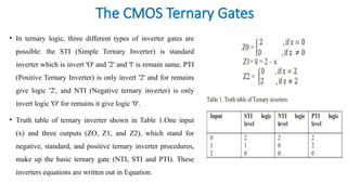
![Logic Gates based on Ternary
• T-NAND, T-NOR, and other ternary logics are also employed in a variety of circuits. Equations are provided
below for certain logics [6].](https://image.slidesharecdn.com/arun-241021091750-6b81ec3b/85/Ternary-Logic-Based-Halfadder-and-full-adder-9-320.jpg)
![Combinational circuits based on Ternary Logic
• If talk about binary half adder two radix number 0 and 1, if want to design 2 bit half adder can only
represent 4outcomes. In ternary use 9 outcomes instead of 4 [1] [18].
• If increase the bit value the difference between binary and ternary is become large. Truth table of THA is
given below in Table.](https://image.slidesharecdn.com/arun-241021091750-6b81ec3b/85/Ternary-Logic-Based-Halfadder-and-full-adder-10-320.jpg)
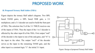
![PROPOSED WORK
• This section includes all the proposed combinational circuits these are Proposed 3:1 TMUX, ternary half adder and ternary
full adder. In this section the design of proposed circuits is presented and their analysis is explained.
A. Proposed 3:1 Ternary multiplexer
The design in Figure operates in a straight forward manner.
Depending on the voltage on the select line S of the multiplexer
(input I0, I1 and 12 of the 1 to 3 decoder), only one Transmission
gate based AND gate output will be operational at one time. For
instance, if the logic on Select line is "1," output out 1 will be high
("2") and the rest will be low (logic"0"). According to the
transmission gate based AND gate truth table shown in Table 2, the
output of transmission AND gates with inputs set to logic 'O' will be
low [20].
Figure: Design of proposed Ternary 3:1 MUX](https://image.slidesharecdn.com/arun-241021091750-6b81ec3b/85/Ternary-Logic-Based-Halfadder-and-full-adder-11-320.jpg)