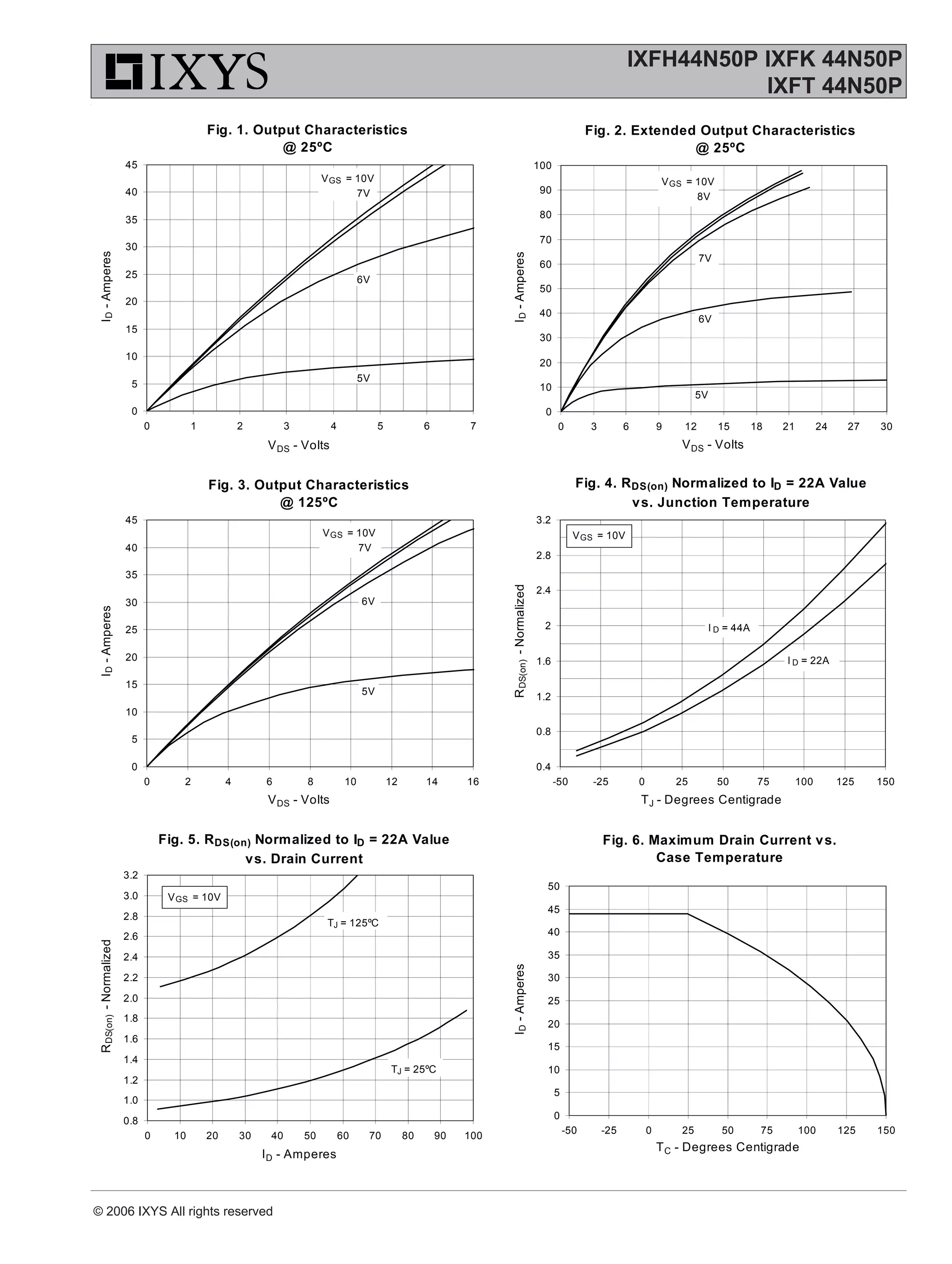
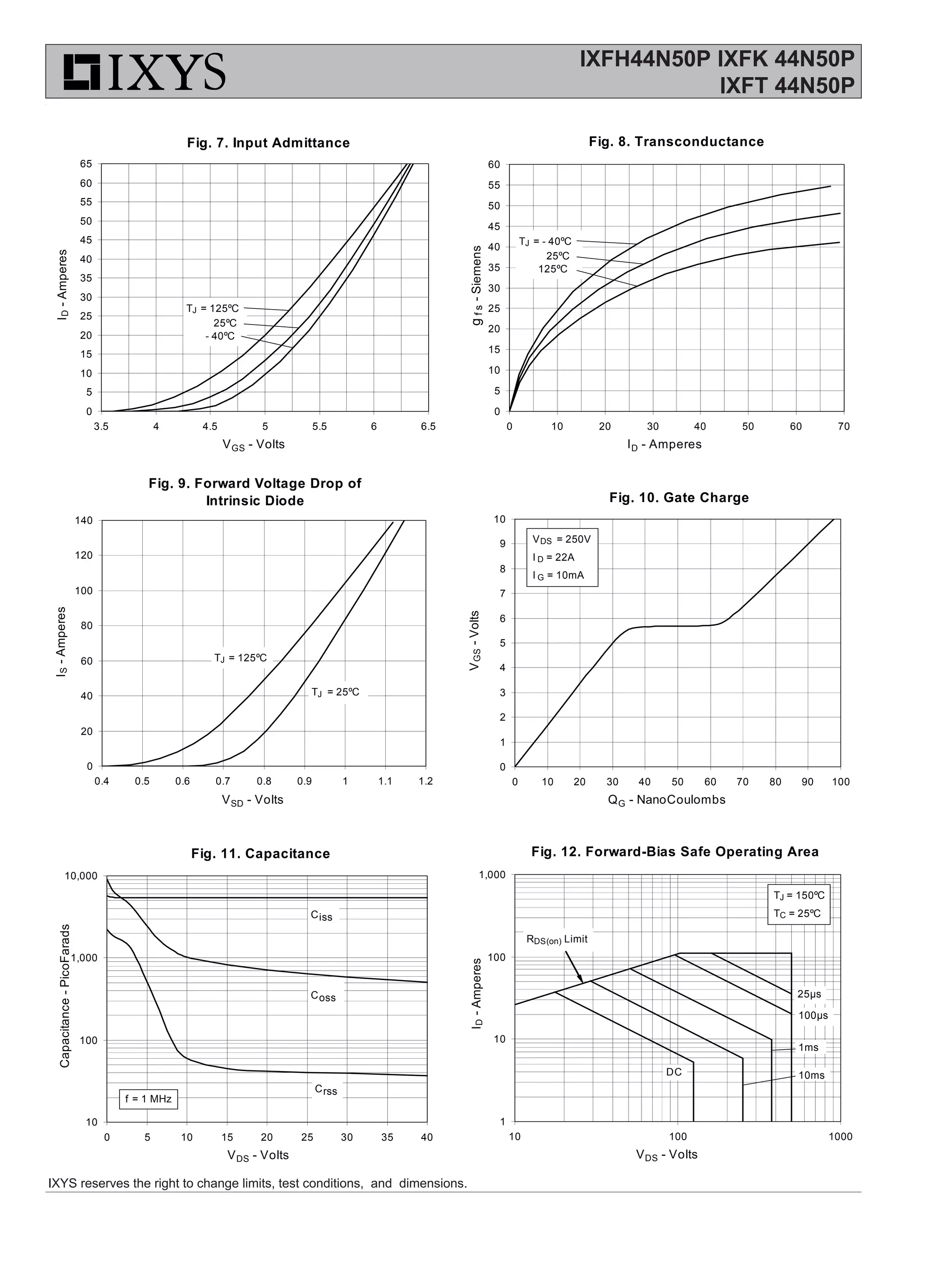
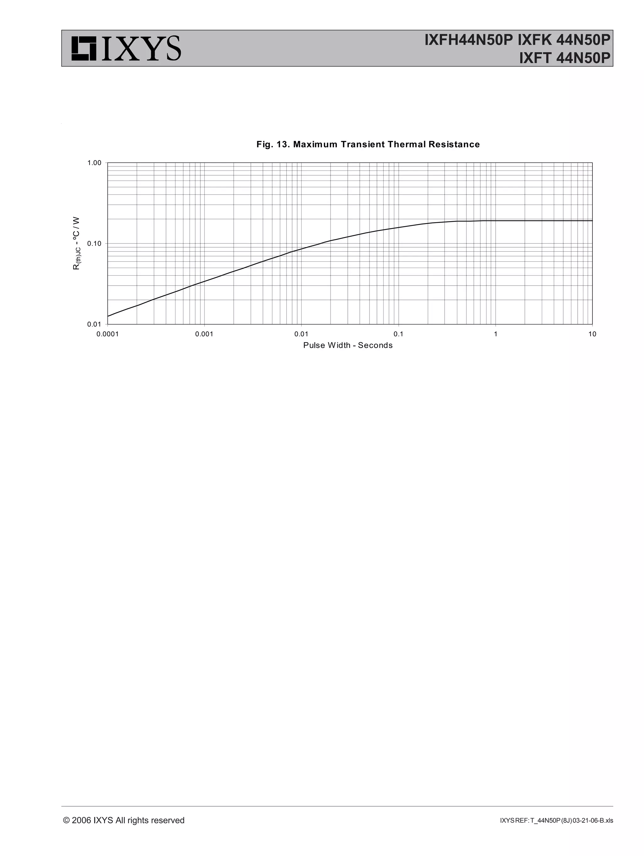
© 2006 IXYS All rights reserved
Symbol Test Conditions Maximum Ratings
VDSS
TJ
= 25° C to 175° C 500 V
VDGR
TJ
= 25° C to 175° C; RGS
= 1 MΩ 500 V
VGSM
Transient ±40 V
VGSM
Continuous ±30 V
ID25
TC
= 25° C 44 A
IDM
TC
= 25° C, pulse width limited by TJM
110 A
IAR
TC
= 25° C 44 A
EAR
TC
= 25° C 55 mJ
EAS
TC
= 25° C 1.7 J
dv/dt IS
≤IDM
, di/dt ≤100 A/µs, VDD
≤VDSS
, 10 V/ns
TJ
≤150° C, RG
= 10 Ω
PD
TC
= 25° C 650 W
TJ
-55 ... +150 °C
TJM
150 °C
Tstg
-55 ... +150 °C
TL
1.6 mm (0.062 in.) from case for 10 s 300 °C
TSOLD
Plastic case for 10 s 260 °C
Md
Mounting torque (TO-247) 1.13/10 Nm/lb.in.
Weight TO-247 6 g
TO-268 5 g
TO-264 10 g
G = Gate D = Drain
S = Source TAB = Drain
DS99366E(03/06)
Symbol Test Conditions Characteristic Values
(TJ
= 25° C, unless otherwise specified) Min. Typ. Max.
BVDSS
VGS
= 0 V, ID
= 250 µA 500 V
VGS(th)
VDS
= VGS
, ID
= 4 mA 3.0 5.0 V
IGSS
VGS
= ±30 VDC
, VDS
= 0 ±10 nA
IDSS
VDS
= VDSS
25 µA
VGS
= 0 V TJ
= 125° C 500 µA
RDS(on)
VGS
= 10 V, ID
= 0.5 ID25
140 mΩ
Pulse test, t ≤300 µs, duty cycle d ≤ 2 %
PolarHVTM
HiPerFET
Power MOSFET
N-Channel Enhancement Mode
Avalanche Rated
Fast Intrinsic Diode
Features
l
International standard packages
l
Unclamped Inductive Switching (UIS)
rated
l
Low package inductance
- easy to drive and to protect
Advantages
l
Easy to mount
l
Space savings
l
High power density
IXFH 44N50P
IXFK 44N50P
IXFT 44N50P
VDSS
= 500 V
ID25
= 44 A
RDS(on)
≤≤≤≤≤ 140 mΩΩΩΩΩ
trr
≤≤≤≤≤ 200 ns
TO-247 AD (IXFH)
(TAB)
TO-268 (IXFT)
G
S
(TAB)
S
G
D
(TAB)
TO-264 (IXFK)
IXYS reserves the right to change limits, test conditions, and dimensions.
IXFH44N50P IXFK 44N50P
IXFT 44N50P
Symbol Test Conditions Characteristic Values
(TJ
= 25° C, unless otherwise specified)
Min. Typ. Max.
gfs
VDS
= 20 V; ID
= 0.5 ID25
, pulse test 20 32 S
Ciss
5440 pF
Coss
VGS
= 0 V, VDS
= 25 V, f = 1 MHz 639 pF
Crss
40 pF
td(on)
28 ns
tr
VGS
= 10 V, VDS
= 0.5 VDSS
, ID
= ID25
29 ns
td(off)
RG
= 3 Ω (External) 85 ns
tf
27 ns
Qg(on)
98 nC
Qgs
VGS
= 10 V, VDS
= 0.5 VDSS
, ID
= 0.5 ID25
35 nC
Qgd
30 nC
RthJC
0.19° C/W
RthCS
(TO-247) 0.21 ° C/W
(TO-264) 0.15 ° C/W
Source-Drain Diode Characteristic Values
(TJ
= 25°C, unless otherwise specified)
Symbol Test Conditions Min. Typ. Max.
IS
VGS
= 0 V 44 A
ISM
Repetitive 110 A
VSD
IF
= IS
, VGS
= 0 V, 1.5 V
Pulse test, t ≤300 µs, duty cycle d≤ 2 %
trr
IF
= 25 A, -di/dt = 100 A/µs 200 ns
QRM
VR
= 100V, VGS
= 0 V 0.6 µC
IRM
6.0 A
IXYS MOSFETs and IGBTs are covered by 4,835,592 4,931,844 5,049,961 5,237,481 6,162,665 6,404,065 B1 6,683,344 6,727,585
one or moreof the following U.S. patents: 4,850,072 5,017,508 5,063,307 5,381,025 6,259,123 B1 6,534,343 6,710,405B2 6,759,692
4,881,106 5,034,796 5,187,117 5,486,715 6,306,728 B1 6,583,505 6,710,463 6,771,478 B2
TO-247 (IXFH) Outline
Terminals: 1 - Gate 2 - Drain
3 - Source Tab - Drain
1 2 3
Dim. Millimeter Inches
Min. Max. Min. Max.
A 4.7 5.3 .185 .209
A1
2.2 2.54 .087 .102
A2
2.2 2.6 .059 .098
b 1.0 1.4 .040 .055
b1
1.65 2.13 .065 .084
b2
2.87 3.12 .113 .123
C .4 .8 .016 .031
D 20.80 21.46 .819 .845
E 15.75 16.26 .610 .640
e 5.20 5.72 0.205 0.225
L 19.81 20.32 .780 .800
L1 4.50 .177
∅P 3.55 3.65 .140 .144
Q 5.89 6.40 0.232 0.252
R 4.32 5.49 .170 .216
S 6.15 BSC 242 BSC
TO-264 (IXFK) Outline
TO-268 (IXFT) Outline
© 2006 IXYS All rights reserved
IXFH44N50P IXFK 44N50P
IXFT 44N50P
Fig. 1. Output Characteristics
@ 25ºC
0
5
10
15
20
25
30
35
40
45
0 1 2 3 4 5 6 7
VDS - Volts
ID-Amperes
VGS = 10V
7V
6V
5V
Fig. 2. Extended Output Characteristics
@ 25ºC
0
10
20
30
40
50
60
70
80
90
100
0 3 6 9 12 15 18 21 24 27 30
VDS - Volts
ID-Amperes
VGS = 10V
8V
7V
5V
6V
Fig. 3. Output Characteristics
@ 125ºC
0
5
10
15
20
25
30
35
40
45
0 2 4 6 8 10 12 14 16
VDS - Volts
ID-Amperes
VGS = 10V
7V
6V
5V
Fig. 4. RDS(on) Normalized to ID = 22A Value
vs. Junction Temperature
0.4
0.8
1.2
1.6
2
2.4
2.8
3.2
-50 -25 0 25 50 75 100 125 150
TJ - Degrees Centigrade
RDS(on)-Normalized
VGS = 10V
I D = 44A
I D = 22A
Fig. 5. RDS(on) Normalized to ID = 22A Value
vs. Drain Current
0.8
1.0
1.2
1.4
1.6
1.8
2.0
2.2
2.4
2.6
2.8
3.0
3.2
0 10 20 30 40 50 60 70 80 90 100
ID - Amperes
RDS(on)-Normalized
VGS = 10V
TJ = 125ºC
TJ = 25ºC
Fig. 6. Maximum Drain Current vs.
Case Temperature
0
5
10
15
20
25
30
35
40
45
50
-50 -25 0 25 50 75 100 125 150
TC - Degrees Centigrade
ID-Amperes
IXYS reserves the right to change limits, test conditions, and dimensions.
IXFH44N50P IXFK 44N50P
IXFT 44N50P
Fig. 7. Input Admittance
0
5
10
15
20
25
30
35
40
45
50
55
60
65
3.5 4 4.5 5 5.5 6 6.5
VGS - Volts
ID-Amperes
TJ = 125ºC
25ºC
- 40ºC
Fig. 8. Transconductance
0
5
10
15
20
25
30
35
40
45
50
55
60
0 10 20 30 40 50 60 70
ID - Amperes
gfs-Siemens
TJ = - 40ºC
25ºC
125ºC
Fig. 9. Forward Voltage Drop of
Intrinsic Diode
0
20
40
60
80
100
120
140
0.4 0.5 0.6 0.7 0.8 0.9 1 1.1 1.2
VSD - Volts
IS-Amperes
TJ = 125ºC
TJ = 25ºC
Fig. 10. Gate Charge
0
1
2
3
4
5
6
7
8
9
10
0 10 20 30 40 50 60 70 80 90 100
QG - NanoCoulombs
VGS-Volts
VDS = 250V
I D = 22A
I G = 10mA
Fig. 11. Capacitance
10
100
1,000
10,000
0 5 10 15 20 25 30 35 40
VDS - Volts
Capacitance-PicoFarads
f = 1 MHz
Ciss
Crss
Coss
Fig. 12. Forward-Bias Safe Operating Area
1
10
100
1,000
10 100 1000
VDS - Volts
ID-Amperes
TJ = 150ºC
TC = 25ºC
25µs
1ms
100µs
RDS(on) Limit
10msDC
© 2006 IXYS All rights reserved
IXFH44N50P IXFK 44N50P
IXFT 44N50P
Fig. 13. Maximum Transient Thermal Resistance
0.01
0.10
1.00
0.0001 0.001 0.01 0.1 1 10
Pulse Width - Seconds
R(th)JC-ºC/W
IXYSREF:T_44N50P(8J)03-21-06-B.xls

Original PolarHV HiPerFET Power MOSFET IXFH44N50P 44N50 TO-3P 44A 500V New IXYS Corporation

  • 1.
    © 2006 IXYSAll rights reserved Symbol Test Conditions Maximum Ratings VDSS TJ = 25° C to 175° C 500 V VDGR TJ = 25° C to 175° C; RGS = 1 MΩ 500 V VGSM Transient ±40 V VGSM Continuous ±30 V ID25 TC = 25° C 44 A IDM TC = 25° C, pulse width limited by TJM 110 A IAR TC = 25° C 44 A EAR TC = 25° C 55 mJ EAS TC = 25° C 1.7 J dv/dt IS ≤IDM , di/dt ≤100 A/µs, VDD ≤VDSS , 10 V/ns TJ ≤150° C, RG = 10 Ω PD TC = 25° C 650 W TJ -55 ... +150 °C TJM 150 °C Tstg -55 ... +150 °C TL 1.6 mm (0.062 in.) from case for 10 s 300 °C TSOLD Plastic case for 10 s 260 °C Md Mounting torque (TO-247) 1.13/10 Nm/lb.in. Weight TO-247 6 g TO-268 5 g TO-264 10 g G = Gate D = Drain S = Source TAB = Drain DS99366E(03/06) Symbol Test Conditions Characteristic Values (TJ = 25° C, unless otherwise specified) Min. Typ. Max. BVDSS VGS = 0 V, ID = 250 µA 500 V VGS(th) VDS = VGS , ID = 4 mA 3.0 5.0 V IGSS VGS = ±30 VDC , VDS = 0 ±10 nA IDSS VDS = VDSS 25 µA VGS = 0 V TJ = 125° C 500 µA RDS(on) VGS = 10 V, ID = 0.5 ID25 140 mΩ Pulse test, t ≤300 µs, duty cycle d ≤ 2 % PolarHVTM HiPerFET Power MOSFET N-Channel Enhancement Mode Avalanche Rated Fast Intrinsic Diode Features l International standard packages l Unclamped Inductive Switching (UIS) rated l Low package inductance - easy to drive and to protect Advantages l Easy to mount l Space savings l High power density IXFH 44N50P IXFK 44N50P IXFT 44N50P VDSS = 500 V ID25 = 44 A RDS(on) ≤≤≤≤≤ 140 mΩΩΩΩΩ trr ≤≤≤≤≤ 200 ns TO-247 AD (IXFH) (TAB) TO-268 (IXFT) G S (TAB) S G D (TAB) TO-264 (IXFK)
  • 2.
    IXYS reserves theright to change limits, test conditions, and dimensions. IXFH44N50P IXFK 44N50P IXFT 44N50P Symbol Test Conditions Characteristic Values (TJ = 25° C, unless otherwise specified) Min. Typ. Max. gfs VDS = 20 V; ID = 0.5 ID25 , pulse test 20 32 S Ciss 5440 pF Coss VGS = 0 V, VDS = 25 V, f = 1 MHz 639 pF Crss 40 pF td(on) 28 ns tr VGS = 10 V, VDS = 0.5 VDSS , ID = ID25 29 ns td(off) RG = 3 Ω (External) 85 ns tf 27 ns Qg(on) 98 nC Qgs VGS = 10 V, VDS = 0.5 VDSS , ID = 0.5 ID25 35 nC Qgd 30 nC RthJC 0.19° C/W RthCS (TO-247) 0.21 ° C/W (TO-264) 0.15 ° C/W Source-Drain Diode Characteristic Values (TJ = 25°C, unless otherwise specified) Symbol Test Conditions Min. Typ. Max. IS VGS = 0 V 44 A ISM Repetitive 110 A VSD IF = IS , VGS = 0 V, 1.5 V Pulse test, t ≤300 µs, duty cycle d≤ 2 % trr IF = 25 A, -di/dt = 100 A/µs 200 ns QRM VR = 100V, VGS = 0 V 0.6 µC IRM 6.0 A IXYS MOSFETs and IGBTs are covered by 4,835,592 4,931,844 5,049,961 5,237,481 6,162,665 6,404,065 B1 6,683,344 6,727,585 one or moreof the following U.S. patents: 4,850,072 5,017,508 5,063,307 5,381,025 6,259,123 B1 6,534,343 6,710,405B2 6,759,692 4,881,106 5,034,796 5,187,117 5,486,715 6,306,728 B1 6,583,505 6,710,463 6,771,478 B2 TO-247 (IXFH) Outline Terminals: 1 - Gate 2 - Drain 3 - Source Tab - Drain 1 2 3 Dim. Millimeter Inches Min. Max. Min. Max. A 4.7 5.3 .185 .209 A1 2.2 2.54 .087 .102 A2 2.2 2.6 .059 .098 b 1.0 1.4 .040 .055 b1 1.65 2.13 .065 .084 b2 2.87 3.12 .113 .123 C .4 .8 .016 .031 D 20.80 21.46 .819 .845 E 15.75 16.26 .610 .640 e 5.20 5.72 0.205 0.225 L 19.81 20.32 .780 .800 L1 4.50 .177 ∅P 3.55 3.65 .140 .144 Q 5.89 6.40 0.232 0.252 R 4.32 5.49 .170 .216 S 6.15 BSC 242 BSC TO-264 (IXFK) Outline TO-268 (IXFT) Outline
  • 3.
    © 2006 IXYSAll rights reserved IXFH44N50P IXFK 44N50P IXFT 44N50P Fig. 1. Output Characteristics @ 25ºC 0 5 10 15 20 25 30 35 40 45 0 1 2 3 4 5 6 7 VDS - Volts ID-Amperes VGS = 10V 7V 6V 5V Fig. 2. Extended Output Characteristics @ 25ºC 0 10 20 30 40 50 60 70 80 90 100 0 3 6 9 12 15 18 21 24 27 30 VDS - Volts ID-Amperes VGS = 10V 8V 7V 5V 6V Fig. 3. Output Characteristics @ 125ºC 0 5 10 15 20 25 30 35 40 45 0 2 4 6 8 10 12 14 16 VDS - Volts ID-Amperes VGS = 10V 7V 6V 5V Fig. 4. RDS(on) Normalized to ID = 22A Value vs. Junction Temperature 0.4 0.8 1.2 1.6 2 2.4 2.8 3.2 -50 -25 0 25 50 75 100 125 150 TJ - Degrees Centigrade RDS(on)-Normalized VGS = 10V I D = 44A I D = 22A Fig. 5. RDS(on) Normalized to ID = 22A Value vs. Drain Current 0.8 1.0 1.2 1.4 1.6 1.8 2.0 2.2 2.4 2.6 2.8 3.0 3.2 0 10 20 30 40 50 60 70 80 90 100 ID - Amperes RDS(on)-Normalized VGS = 10V TJ = 125ºC TJ = 25ºC Fig. 6. Maximum Drain Current vs. Case Temperature 0 5 10 15 20 25 30 35 40 45 50 -50 -25 0 25 50 75 100 125 150 TC - Degrees Centigrade ID-Amperes
  • 4.
    IXYS reserves theright to change limits, test conditions, and dimensions. IXFH44N50P IXFK 44N50P IXFT 44N50P Fig. 7. Input Admittance 0 5 10 15 20 25 30 35 40 45 50 55 60 65 3.5 4 4.5 5 5.5 6 6.5 VGS - Volts ID-Amperes TJ = 125ºC 25ºC - 40ºC Fig. 8. Transconductance 0 5 10 15 20 25 30 35 40 45 50 55 60 0 10 20 30 40 50 60 70 ID - Amperes gfs-Siemens TJ = - 40ºC 25ºC 125ºC Fig. 9. Forward Voltage Drop of Intrinsic Diode 0 20 40 60 80 100 120 140 0.4 0.5 0.6 0.7 0.8 0.9 1 1.1 1.2 VSD - Volts IS-Amperes TJ = 125ºC TJ = 25ºC Fig. 10. Gate Charge 0 1 2 3 4 5 6 7 8 9 10 0 10 20 30 40 50 60 70 80 90 100 QG - NanoCoulombs VGS-Volts VDS = 250V I D = 22A I G = 10mA Fig. 11. Capacitance 10 100 1,000 10,000 0 5 10 15 20 25 30 35 40 VDS - Volts Capacitance-PicoFarads f = 1 MHz Ciss Crss Coss Fig. 12. Forward-Bias Safe Operating Area 1 10 100 1,000 10 100 1000 VDS - Volts ID-Amperes TJ = 150ºC TC = 25ºC 25µs 1ms 100µs RDS(on) Limit 10msDC
  • 5.
    © 2006 IXYSAll rights reserved IXFH44N50P IXFK 44N50P IXFT 44N50P Fig. 13. Maximum Transient Thermal Resistance 0.01 0.10 1.00 0.0001 0.001 0.01 0.1 1 10 Pulse Width - Seconds R(th)JC-ºC/W IXYSREF:T_44N50P(8J)03-21-06-B.xls