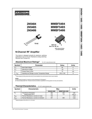
SlideShare a Scribd company logo
G
D
S
2N5484
2N5485
2N5486
MMBF5484
MMBF5485
MMBF5486
N-Channel RF Amplifier
This device is designed primarily for electronic switching
applications such as low On Resistance analog switching.
Sourced from Process 50.
Absolute Maximum Ratings* TA = 25°C unless otherwise noted
Symbol Parameter Value Units
VDG Drain-Gate Voltage 25 V
VGS Gate-Source Voltage - 25 V
IGF Forward Gate Current 10 mA
TJ ,Tstg Operating and Storage Junction Temperature Range -55 to +150 °C
G
S
D
TO-92
SOT-23
Mark: 6B / 6M / 6H
*These ratings are limiting values above which the serviceability of any semiconductor device may be impaired.
NOTES:
1) These ratings are based on a maximum junction temperature of 150 degrees C.
2) These are steady state limits. The factory should be consulted on applications involving pulsed or low duty cycle operations.
Thermal Characteristics TA = 25°C unless otherwise noted
*Device mounted on FR-4 PCB 1.6" X 1.6" X 0.06."
1997 Fairchild Semiconductor Corporation
NOTE: Source & Drain
are interchangeable
2N5484/5485/5486/MMBF5484/5485/5486
Symbol Characteristic Max Units
2N5484-5486 *MMBF5484-5486
PD Total Device Dissipation
Derate above 25°C
350
2.8
225
1.8
mW
mW/°C
RθJC Thermal Resistance, Junction to Case 125 °C/W
RθJA Thermal Resistance, Junction to Ambient 357 556 °C/W
5
Electrical Characteristics TA = 25°C unless otherwise noted
OFF CHARACTERISTICS
Symbol Parameter Test Conditions Min Typ Max Units
ONCHARACTERISTICS
V(BR)GSS Gate-Source Breakdown Voltage IG = - 1.0 µA, VDS = 0 - 25 V
IGSS Gate Reverse Current VGS = - 20 V, VDS = 0
VGS= - 20 V, VDS= 0, TA= 100°C
- 1.0
- 0.2
nA
µA
VGS(off) Gate-Source Cutoff Voltage VDS = 15 V, ID = 10 nA 5484
5485
5486
- 0.3
- 0.5
- 2.0
- 3.0
- 4.0
- 6.0
V
V
V
IDSS Zero-Gate Voltage Drain Current* VDS = 15 V, VGS = 0 5484
5485
5486
1.0
4.0
8.0
5.0
10
20
mA
mA
mA
SMALL SIGNAL CHARACTERISTICS
gfs Forward Transfer Conductance VDS = 15 V, VGS = 0, f = 1.0 kHz
5484
5485
5486
3000
3500
4000
6000
7000
8000
µmhos
µmhos
µmhos
Re(yis) Input Conductance VDS = 15 V, VGS = 0, f = 100 MHz
5484
VDS = 15 V, VGS = 0, f = 400 MHz
5485 / 5486
100
1000
µmhos
µmhos
gos Output Conductance VDS = 15 V, VGS = 0, f = 1.0 kHz
5484
5485
5486
50
60
75
µmhos
µmhos
µmhos
Re(yos) Output Conductance VDS = 15 V, VGS = 0, f = 100 MHz
5484
VDS = 15 V, VGS = 0, f = 400 MHz
5485 / 5486
75
100
µmhos
µmhos
Re(yfs) Forward Transconductance VDS = 15 V, VGS = 0, f = 100 MHz
5484
VDS = 15 V, VGS = 0, f = 400 MHz
5485
5486
2500
3000
3500
µmhos
µmhos
µmhos
Ciss Input Capacitance VDS = 15 V, VGS = 0, f = 1.0 MHz 5.0 pF
Crss Reverse Transfer Capacitance VDS = 15 V, VGS = 0, f = 1.0 MHz 1.0 pF
Coss Output Capacitance VDS = 15 V, VGS = 0, f = 1.0 MHz 2.0 pF
NF Noise Figure VDS= 15 V, RG = 1.0 kΩ,
f = 100 MHz 5484
VDS= 15 V, RG = 1.0 kΩ,
f = 400 MHz 5484
VDS= 15 V , RG = 1.0 kΩ,
f = 100 MHz 5485 / 5486
VDS= 15 V, RG = 1.0 kΩ,
f = 400 MHz 5485 / 5486
4.0
3.0
2.0
4.0
dB
dB
dB
dB
*Pulse Test: Pulse Width ≤ 300 ms, Duty Cycle ≤ 2%
2N5484/5485/5486/MMBF5484/5485/5486
N-Channel RF Amplifier
(continued)
2N5484/5485/5486/MMBF5484/5485/5486
Typical Characteristics
°°°°°
Transfer Characteristics
-5-4-3-2-10
0
4
8
12
16
20
V - GATE-SOURCE VOLTAGE(V)
I-DRAINCURRENT(mA)D
GS(OFF)V = -4.5V V = 15VDS
T = +25 CA
O
-2.5 V
T = -55 C
O
A
T = +125 CA
O
T = -55 C
O
A
T = +25 CA
O
T = +125 CA
O
GS
Channel Resistance vs Temperature
-50 0 50 100 150
10
20
30
50
100
200
300
500
1000
T - AMBIENT TEMPERATURE ( C)
r-DRAINONRESISTANCE()Ω
V = -1.0VGS(OFF)
-2.5 V
-5.0V
-8.0 V
V = 100mVDS
V = 0 V
GS
DS
A
Transconductance
Characteristics
-5-4-3-2-10
0
1
2
3
4
5
6
7
V - GATE-SOURCE VOLTAGE(V)
gfs--TRANSCONDUCTANCE(mmhos)
V = -4.5VGS(OFF)
V = 15VDS
T = +25 CA
O
-2.5 V
T = -55 C
O
A
T = +125 CA
O
T = -55 C
O
A
T = +25 CA
O
T = +125 CA
O
GS
Common Drain-Source
Characteristics
0 0.2 0.4 0.6 0.8 1
0
1
2
3
4
5
V - DRAIN-SOURCE VOLTAGE(V)
I--DRAINCURRENT(mA)
V
=
0V
GS
-2.5V
DS
-0.5V
-4.0V
-2.0V
-1.0V
-3.5V
-3.0V
-1.5V
T = +25 CA
O
TYP V = -5.0VGS(OFF)
D
Transconductance
Parameter Interactions
1 2 3 5 7 10
10
20
1
2
3
5
10
20
30
50
100
V - GATE-SOURCE VOLTAGE(V)
r--DRAIN"ON"RESISTANCE()
gfs---TRANSCONDUCTANCE(mmhos)
GS
I--DRAINCURRENT(mA)
DSS
DSΩ
gfs, I @ V = 15 V, V = 0 PULSEGSDSDSS
r @ V = 100mV, V = 0GSDSDS
V @ V = 15V, I = 1nAGS(OFF) GS D
- -----
Output Conductance vs
Drain Current
0.01 0.02 0.05 0.1 0.2 0.5 1 2 5 10
0.1
0.5
1
5
10
20
I -- DRAIN CURRENT (mA)
gos--OUTPUTCONDUCTANCE(umhos)
D
15
10
T = +25 CA
O
f = 1.0 kHz
15
10
5
20
15V
10V
5.0V
20V
20
V = 5v
DG
V = -5.5VGS(OFF)
V = -3.5VGS(OFF)
V = -1.5VGS(OFF)
N-Channel RF Amplifier
(continued)
5
Noise Voltage vs Frequency
0.01 0.03 0.1 0.3 1 3 10 30 100
1
5
10
f -- FREQUENCY (kHz)
e-NOISEVOLTAGE(nV/Hz)
V = 15VDG
BW = 6.0 Hz @ f = 10 Hz, 100 Hz
= 0.2 f @ f > 1.0 kHz
I = 0.5 mAD
I = 3 mAD
n
Noise Figure Frequency
10 20 30 50 100 200 300 500 1000
0
1
2
3
4
5
f -- FREQUENCY (MHz)
NF--NOISEFIGURE(dB)
V = 15VDS
I = 5.0 mA
R = 1.0 k
T = +25 CA
O
Ω
D
g
Typical Characteristics (continued)
Power Dissipation vs.
Ambient Temperature
0 25 50 75 100 125 150
0
50
100
150
200
250
300
350
TEMPERATURE ( C)
P-POWERDISSIPATION(mW)
º
D
SOT-23
TO-92
Capacitance vs Voltage
-20-15-10-50
1
5
10
V -- GATE-SOURCE VOLTAGE(V)
C(C)--CAPACITANCE(pF)
GS
isrs
C ( V = 0 V)
C ( V = 15 V)DS
DS
is
rs
f = 0.1 - 1.0 MHz
Transconductance vs
Drain Current
0.1
0.5
1
5
10
gfs--TRANSCONDUCTANCE(mmhos)
0.01 0.02 0.05 0.1 0.2 0.5 1 2 5 10
I - DRAIN CURRENT (mA)D
V = - 5VGS(OFF)
V = - 1.5VGS(OFF)
T = -55 C
O
A
T = +25 CA
O
T = +125 CA
O
T = -55 C
O
A
T = +25 CA
O
T = +125 CA
O
V = 15V
f = 1.0 kHz
DG
2N5484/5485/5486/MMBF5484/5485/5486
N-Channel RF Amplifier
(continued)
2N5484/5485/5486/MMBF5484/5485/5486
Common Source Characteristics
Input Admittance
100 200 300 500 700 1000
1
5
10
f -- FREQUENCY (MHz)
Y--INPUTADMITTANCE(mmhos)
V = 15V
V = 0GS
DS
(CS)
g iss
iss
b iss
Output Admittance
100 200 300 500 700 1000
1
f -- FREQUENCY (MHz)
Y--OUTPUTCONDUCTANCE(mmhos)
V = 15V
V = 0GS
DS
(CS)
OSS
b (x 10)OSS
g OSS
Forward Transadmittance
100 200 300 500 700 1000
1
5
10
f -- FREQUENCY (MHz)
Y--FORWARDTRANSFER(mmhos)
V = 15V
V = 0GS
DS
(CS)
-b fss
fss
+g
fss
Reverse Transadmittance
100 200 300 500 700 1000
1
5
10
f -- FREQUENCY (MHz)
Y--REVERSETRANSFER(mmhos)rss
V = 15V
V = 0GS
DS
(CS)
- b
-g ( X 0.1)rss
rss
N-Channel RF Amplifier
(continued)
5
Common Gate Characteristics
Input Admittance
100 200 300 500 700 1000
1
5
10
f -- FREQUENCY (MHz)
Y--INPUTADMITTANCE(mmhos)
V = 15V
V = 0GS
DS
(CG)
g igs
igs
b igs
Forward Transadmittance
100 200 300 500 700 1000
1
5
10
f -- FREQUENCY (MHz)
Y--FORWARDTRANSFER(mmhos)
V = 15V
V = 0GS
DS
(CG)
-b fgs
fgs
+g fgs
Reverse Transadmittance
100 200 300 500 700 1000
1
f -- FREQUENCY (MHz)
Y--REVERSETRANSFER(mmhos)rgs
V = 15V
V = 0GS
DS
(CG)
g
rgs
- brgs
Output Admittance
100 200 300 500 700 1000
1
f -- FREQUENCY (MHz)
Y--OUTPUTCONDUCTANCE(mmhos)
V = 15V
V = 0GS
DS
(CG)
ogs
b (x 10)OgS
g Ogs
2N5484/5485/5486/MMBF5484/5485/5486
N-Channel RF Amplifier
(continued)
TO-92 Tape and Reel Data
March 2001, Rev. B1©2001 Fairchild Semiconductor Corporation
TO-92 Packaging
Configuration: Figure 1.0
AMMO PACK OPTION
See Fig 3.0 for 2 Ammo
Pack Options
2000 units per
EO70 box for
std option
FSCINT Label
530mm x 130mm x 83mm
Intermediate box
10,000 units maximum
per intermediate box
for std option
FSCINT Label
114mm x 102mm x 51mm
Immediate Box
Anti-static
Bubble Sheets
(TO-92) BULK PACKING INFORMATION
EOL
CODE
DESCRIPTION
LEADCLIP
DIMENSION
QUANTITY
J18Z TO-18 OPTION STD NO LEAD CLIP 2.0 K / BOX
J05Z TO-5 OPTION STD NO LEAD CLIP 1.5 K / BOX
NO EOL
CODE
TO-92 STANDARD
STRAIGHT FOR: PKG 92,
NO LEADCLIP 2.0 K / BOX
BULK OPTION
See Bulk Packing
Information table
375mm x 267mm x 375mm
Intermediate Box
FSCINT
Label
Customized
Label
333mm x 231mm x 183mm
Intermediate Box
FSCINT
Label
Customized
Label
TO-92 TNR/AMMO PACKING INFROMATION
Packing Style Quantity EOL code
Reel A 2,000 D26Z
E 2,000 D27Z
Ammo M 2,000 D74Z
P 2,000 D75Z
Unit weight = 0.22 gm
Reel weight with components = 1.04 kg
Ammo weight with components = 1.02 kg
Max quantity per intermediate box = 10,000 units
F63TNR
Label
5 Ammo boxes per
Intermediate Box
Customized
Label
327mm x 158mm x 135mm
Immediate Box
LOT: CBVK741B019
NSID: PN2222N
D/C1: D9842 SPEC REV: B2
SPEC:
QTY: 10000
QA REV:
FAIRCHILD SEMICONDUCTOR CORPORATION HTB:B
(FSCINT)
F63TNR
Label
Customized
Label
5 Reels per
Intermediate Box
TAPE and REEL OPTION
See Fig 2.0 for various
Reeling Styles
LOT: CBVK741B019
FSID: PN222N
D/C1: D9842 QTY1: SPEC REV:
SPEC:
QTY: 2000
D/C2: QTY2: CPN:
N/F: F (F63TNR)3
F63TNR Label sample
FSCINT Label sample
C
5 EO70 boxes per
intermediate Box
ustomized
Label
94 (NON PROELECTRON
SERIES), 96
L34Z TO-92 STANDARD
STRAIGHT FOR: PKG 94
NO LEADCLIP 2.0 K / BOX
(PROELECTRON SERIES
BCXXX, BFXXX, BSRXXX),
97, 98
TO-92 Tape and Reel Data, continued
September 1999, Rev. B
TO-92 Reeling Style
Configuration: Figure 2.0
Style “A”, D26Z, D70Z (s/h)
Machine Option “A” (H)
Style “E”, D27Z, D71Z (s/h)
Machine Option “E” (J)
FIRST WIRE OFF IS EMITTER
ADHESIVE TAPE IS ON THE TOP SIDE
FLAT OF TRANSISTOR IS ON BOTTOM
ORDER STYLE
D75Z (P)
FIRST WIRE OFF IS COLLECTOR
ADHESIVE TAPE IS ON THE TOP SIDE
FLAT OF TRANSISTOR IS ON TOP
ORDER STYLE
D74Z (M)
TO-92 Radial Ammo Packaging
Configuration: Figure 3.0
FIRST WIRE OFF IS EMITTER (ON PKG. 92)
ADHESIVE TAPE IS ON BOTTOM SIDE
FLAT OF TRANSISTOR IS ON BOTTOM
FIRST WIRE OFF IS COLLECTOR (ON PKG. 92)
ADHESIVE TAPE IS ON BOTTOM SIDE
FLAT OF TRANSISTOR IS ON TOP
ITEM DESCRIPTION
Base of Package to Lead Bend
Component Height
Lead Clinch Height
Component Base Height
Component Alignment ( side/side )
Component Alignment ( front/back )
Component Pitch
Feed Hole Pitch
Hole Center to First Lead
Hole Center to Component Center
Lead Spread
Lead Thickness
Cut Lead Length
Taped Lead Length
Taped Lead Thickness
Carrier Tape Thickness
Carrier Tape Width
Hold - down Tape Width
Hold - down Tape position
Feed Hole Position
Sprocket Hole Diameter
Lead Spring Out
SYMBOL
b
Ha
HO
H1
Pd
Hd
P
PO
P1
P2
F1/F2
d
L
L1
t
t1
W
WO
W1
W2
DO
S
DIMENSION
0.098 (max)
0.928 (+/- 0.025)
0.630 (+/- 0.020)
0.748 (+/- 0.020)
0.040 (max)
0.031 (max)
0.500 (+/- 0.020)
0.500 (+/- 0.008)
0.150 (+0.009, -0.010)
0.247 (+/- 0.007)
0.104 (+/- 0 .010)
0.018 (+0.002, -0.003)
0.429 (max)
0.209 (+0.051, -0.052)
0.032 (+/- 0.006)
0.021 (+/- 0.006)
0.708 (+0.020, -0.019)
0.236 (+/- 0.012)
0.035 (max)
0.360 (+/- 0.025)
0.157 (+0.008, -0.007)
0.004 (max)
Note : All dimensions are in inches.
ITEM DESCRIPTION SYSMBOL MINIMUM MAXIMUM
Reel Diameter D1 13.975 14.025
Arbor Hole Diameter (Standard) D2 1.160 1.200
(Small Hole) D2 0.650 0.700
Core Diameter D3 3.100 3.300
Hub Recess Inner Diameter D4 2.700 3.100
Hub Recess Depth W1 0.370 0.570
Flange to Flange Inner Width W2 1.630 1.690
Hub to Hub Center Width W3 2.090
Note: All dimensions are inches
TO-92 Tape and Reel Taping
Dimension Configuration: Figure 4.0
Ha
H1 HO
PO
P2
P1 F1
DO
P Pd
b
d
L1
L
S
WO
W2
W
t
t1
Hd
W1
TO-92 Reel
Configuration: Figure 5.0
User Direction of Feed
SEN SITIVE D EVICES
ELECTROSTATIC
D1
D3
Customized Label
W2
W1
W3
F63TNR Label
D4
D2
TO-92 Tape and Reel Data, continued
July 1999, Rev. A
TO-92 (FS PKG Code 92, 94, 96)
TO-92 Package Dimensions
January 2000, Rev. B
1:1
Scale 1:1 on letter size paper
Dimensions shown below are in:
inches [millimeters]
Part Weight per unit (gram): 0.1977
©2000 Fairchild Semiconductor International
SOT-23 Packaging
Configuration: Figure 1.0
Components
Leader Tape
500mm minimumor
125 empty pockets
Trailer Tape
300mm minimumor
75 empty pockets
SOT-23 Tape Leader and Trailer
Configuration: Figure 2.0
Cover Tape
Carrier Tape
Note/Comments
PackagingOption
SOT-23 PackagingInformation
Standard
(no flow code)
D87Z
Packagingtype
Reel Size
TNR
7" Dia
TNR
13"
Qty per Reel/Tube/Bag 3,000 10,000
Box Dimension (mm) 187x107x183 343x343x64
Max qty per Box 24,000 30,000
Weight per unit (gm) 0.0082 0.0082
Weight per Reel (kg) 0.1175 0.4006
Human readable
Label
Human Readable Label
Human Readable Label sample
343mmx 342mmx 64mm
Intermediate box for L87Z Option
187mmx 107mmx 183mm
Intermediate Box forStandard Option
SOT-23 Unit Orientation
3P 3P 3P 3P
Human Readable
Label
Customized Label
Embossed
Carrier Tape
Antistatic Cover Tape
Packaging Description:
SOT-23
made from a dissipative (carbon filled) polycarbonate
resin. The cover tape is a multilayer film (Heat Activated
Adhesive in nature) primarily composed of polyester film,
adhesive layer, sealant, and anti-static sprayed agent.
These reeled parts in standard option are shipped with
3,000 units per 7" or 177cm diameter reel. The reels are
dark bluein color and is made of polystyrene plastic (anti-
static coated). Other option comes in 10,000 units per 13"
or 330cm diameter reel. This and some other options are
described in the Packaging Information table.
These full reels are individually labeled and placed inside
a standard intermediate made of recyclable corrugated
brown paper with aFairchild logo printing. One pizza box
contains eight reels maximum. And these intermediate
boxes are placed inside a labeled shipping box which
comesin different sizes depending on the number of parts
shipped.
parts are shipped in tape. The carrier tape is
SOT-23 Tape and Reel Data
September 1999, Rev. C©2000 Fairchild Semiconductor International
Dimensions are in millimeter
Pkg type A0 B0 W D0 D1 E1 E2 F P1 P0 K0 T Wc Tc
SOT-23
(8mm)
3.15
+/-0.10
2.77
+/-0.10
8.0
+/-0.3
1.55
+/-0.05
1.125
+/-0.125
1.75
+/-0.10
6.25
min
3.50
+/-0.05
4.0
+/-0.1
4.0
+/-0.1
1.30
+/-0.10
0.228
+/-0.013
5.2
+/-0.3
0.06
+/-0.02
Dimensions are in inches and millimeters
Tape Size
Reel
Option
Dim A Dim B Dim C Dim D Dim N Dim W1 Dim W2 Dim W3 (LSL-USL)
8mm 7" Dia
7.00
177.8
0.059
1.5
512 +0.020/-0.008
13 +0.5/-0.2
0.795
20.2
2.165
55
0.331 +0.059/-0.000
8.4 +1.5/0
0.567
14.4
0.311 – 0.429
7.9 – 10.9
8mm 13" Dia
13.00
330
0.059
1.5
512 +0.020/-0.008
13 +0.5/-0.2
0.795
20.2
4.00
100
0.331 +0.059/-0.000
8.4 +1.5/0
0.567
14.4
0.311 – 0.429
7.9 – 10.9
See detail AA
Dim A
max
13" Diameter Option
7"Diameter Option
Dim A
Max
See detail AA
W3
W2 max Measured at Hub
W1 Measured at Hub
Dim N
Dim D
min
Dim C
B Min
DETAIL AA
Notes: A0, B0, and K0 dimensions are determined with respect to the EIA/Jedec RS-481
rotational and lateral movement requirements (see sketches A, B, and C).
20 deg maximum component rotation
0.5mm
maximum
0.5mm
maximum
Sketch C (Top View)
Component lateral movement
Typical
component
cavity
center line
20 deg maximum
Typical
component
center line
B0
A0
Sketch B (Top View)
Component Rotation
Sketch A (Side or Front Sectional View)
Component Rotation
User Direction of Feed
SOT-23 Embossed Carrier Tape
Configuration: Figure 3.0
SOT-23 Reel Configuration: Figure 4.0
P1 A0
D1
F W
E1
E2
Tc
Wc
K0
T
B0
D0P0 P2
SOT-23 Tape and Reel Data, continued
September 1999, Rev. C
SOT-23 (FS PKG Code 49)
SOT-23 Package Dimensions
September 1998, Rev. A1
1:1
Scale 1:1 on letter size paper
Dimensions shown below are in:
inches [millimeters]
Part Weight per unit (gram): 0.0082
©2000 Fairchild Semiconductor International
TRADEMARKS
The following are registered and unregistered trademarks Fairchild Semiconductor owns or is authorized to use and is
not intended to be an exhaustive list of all such trademarks.
LIFE SUPPORT POLICY
FAIRCHILD’S PRODUCTS ARE NOT AUTHORIZED FOR USE AS CRITICAL COMPONENTS IN LIFE SUPPORT
DEVICESORSYSTEMSWITHOUTTHEEXPRESSWRITTENAPPROVALOFFAIRCHILDSEMICONDUCTORCORPORATION.
As used herein:
1. Life support devices or systems are devices or
systems which, (a) are intended for surgical implant into
the body, or (b) support or sustain life, or (c) whose
failure to perform when properly used in accordance
with instructions for use provided in the labeling, can be
reasonably expected to result in significant injury to the
user.
2. A critical component is any component of a life
support device or system whose failure to perform can
be reasonably expected to cause the failure of the life
support device or system, or to affect its safety or
effectiveness.
PRODUCT STATUS DEFINITIONS
Definition of Terms
Datasheet Identification Product Status Definition
Advance Information
Preliminary
No Identification Needed
Obsolete
This datasheet contains the design specifications for
product development. Specifications may change in
any manner without notice.
This datasheet contains preliminary data, and
supplementary data will be published at a later date.
Fairchild Semiconductor reserves the right to make
changes at any time without notice in order to improve
design.
This datasheet contains final specifications. Fairchild
Semiconductor reserves the right to make changes at
any time without notice in order to improve design.
This datasheet contains specifications on a product
that has been discontinued by Fairchild semiconductor.
The datasheet is printed for reference information only.
Formative or
In Design
First Production
Full Production
Not In Production
DISCLAIMER
FAIRCHILD SEMICONDUCTOR RESERVES THE RIGHT TO MAKE CHANGES WITHOUT FURTHER
NOTICE TOANY PRODUCTS HEREIN TO IMPROVE RELIABILITY, FUNCTION OR DESIGN. FAIRCHILD
DOES NOTASSUMEANY LIABILITYARISING OUT OF THE APPLICATION OR USE OFANY PRODUCT
OR CIRCUIT DESCRIBED HEREIN; NEITHER DOES IT CONVEY ANY LICENSE UNDER ITS PATENT
RIGHTS, NOR THE RIGHTS OF OTHERS.
PowerTrench
QFET™
QS™
QT Optoelectronics™
Quiet Series™
SILENT SWITCHER
SMART START™
SuperSOT™-3
SuperSOT™-6
SuperSOT™-8
FASTr™
GlobalOptoisolator™
GTO™
HiSeC™
ISOPLANAR™
MICROWIRE™
OPTOLOGIC™
OPTOPLANAR™
PACMAN™
POP™
Rev. G

ACEx™
Bottomless™
CoolFET™
CROSSVOLT™
DOME™
E2
CMOSTM
EnSignaTM
FACT™
FACT Quiet Series™
FAST
SyncFET™
TinyLogic™
UHC™
VCX™



More Related Content

What's hot

Original PNP Transistors PZT2907A PZT2907 2907 P2F SOT22-3 New On Semiconductor
Original PNP Transistors PZT2907A PZT2907 2907 P2F SOT22-3 New On SemiconductorOriginal PNP Transistors PZT2907A PZT2907 2907 P2F SOT22-3 New On Semiconductor
Original PNP Transistors PZT2907A PZT2907 2907 P2F SOT22-3 New On Semiconductorauthelectroniccom
 
Original Dual P-Channel Mosfet RF7316TRPBF IRF7316 F7316 7316 SOP-8 New IR
Original Dual P-Channel Mosfet RF7316TRPBF IRF7316 F7316 7316 SOP-8 New IROriginal Dual P-Channel Mosfet RF7316TRPBF IRF7316 F7316 7316 SOP-8 New IR
Original Dual P-Channel Mosfet RF7316TRPBF IRF7316 F7316 7316 SOP-8 New IRAUTHELECTRONIC
 
Original Mosfet N FDPF8N50NZ 8N50 8N50NZ 10V 4A TO-220 New Fairchild
Original Mosfet N FDPF8N50NZ 8N50 8N50NZ 10V 4A TO-220 New FairchildOriginal Mosfet N FDPF8N50NZ 8N50 8N50NZ 10V 4A TO-220 New Fairchild
Original Mosfet N FDPF8N50NZ 8N50 8N50NZ 10V 4A TO-220 New FairchildAUTHELECTRONIC
 
Original N-channel Mosfet PHB108NQ03LT PHB108 NQ03LT 25V 75A TO-252 New NXP
Original N-channel Mosfet PHB108NQ03LT PHB108 NQ03LT 25V 75A TO-252 New  NXPOriginal N-channel Mosfet PHB108NQ03LT PHB108 NQ03LT 25V 75A TO-252 New  NXP
Original N-channel Mosfet PHB108NQ03LT PHB108 NQ03LT 25V 75A TO-252 New NXPAUTHELECTRONIC
 
Original IGBT STGP6NC60HD GP6NC60 6N60 600V 15A TO-220 New STMicroelectronics
Original IGBT STGP6NC60HD GP6NC60 6N60 600V 15A TO-220 New STMicroelectronicsOriginal IGBT STGP6NC60HD GP6NC60 6N60 600V 15A TO-220 New STMicroelectronics
Original IGBT STGP6NC60HD GP6NC60 6N60 600V 15A TO-220 New STMicroelectronicsAUTHELECTRONIC
 
Original IGBT STGP6NC60HD 6N60 600V 15A TO-220 New STMicroelectronics
Original IGBT STGP6NC60HD 6N60 600V 15A TO-220 New STMicroelectronicsOriginal IGBT STGP6NC60HD 6N60 600V 15A TO-220 New STMicroelectronics
Original IGBT STGP6NC60HD 6N60 600V 15A TO-220 New STMicroelectronicsauthelectroniccom
 
Original N-Channel Mosfet STF9NK90Z F9NK90Z 8A 900V TO-220F New STMicroelectr...
Original N-Channel Mosfet STF9NK90Z F9NK90Z 8A 900V TO-220F New STMicroelectr...Original N-Channel Mosfet STF9NK90Z F9NK90Z 8A 900V TO-220F New STMicroelectr...
Original N-Channel Mosfet STF9NK90Z F9NK90Z 8A 900V TO-220F New STMicroelectr...AUTHELECTRONIC
 
Kollmorgen xt 150 specsheet
Kollmorgen  xt 150 specsheetKollmorgen  xt 150 specsheet
Kollmorgen xt 150 specsheetElectromate
 
Mrf6 s18100n pwrmosfet
Mrf6 s18100n pwrmosfetMrf6 s18100n pwrmosfet
Mrf6 s18100n pwrmosfetdreamboxsat
 
Original N Channel Mosfet PHP45N03LTA PHP45N03LT 45N03LTA 45N03 TO-220 New
Original N Channel Mosfet PHP45N03LTA PHP45N03LT 45N03LTA 45N03 TO-220 NewOriginal N Channel Mosfet PHP45N03LTA PHP45N03LT 45N03LTA 45N03 TO-220 New
Original N Channel Mosfet PHP45N03LTA PHP45N03LT 45N03LTA 45N03 TO-220 NewAUTHELECTRONIC
 
Original Opto LTV-354T LTV354T 354T 354 SOP-4 New
Original Opto LTV-354T LTV354T 354T 354 SOP-4 NewOriginal Opto LTV-354T LTV354T 354T 354 SOP-4 New
Original Opto LTV-354T LTV354T 354T 354 SOP-4 NewAUTHELECTRONIC
 
Original P Channel Mosfet IRF9Z34 IRF9Z34N IRF9Z34NPBF 9Z34 60V 18A TO 220 New
Original P Channel Mosfet IRF9Z34 IRF9Z34N IRF9Z34NPBF 9Z34 60V 18A TO 220 NewOriginal P Channel Mosfet IRF9Z34 IRF9Z34N IRF9Z34NPBF 9Z34 60V 18A TO 220 New
Original P Channel Mosfet IRF9Z34 IRF9Z34N IRF9Z34NPBF 9Z34 60V 18A TO 220 NewAUTHELECTRONIC
 
Original Mosfet N-Channel SVF740T 740 400V 10A TO-220 New
Original Mosfet N-Channel SVF740T 740 400V 10A TO-220 NewOriginal Mosfet N-Channel SVF740T 740 400V 10A TO-220 New
Original Mosfet N-Channel SVF740T 740 400V 10A TO-220 NewAUTHELECTRONIC
 
Original N-channel TrenchMOS transistor PHB95N03LT 95N03LT 25V 75A SOT-404 Ne...
Original N-channel TrenchMOS transistor PHB95N03LT 95N03LT 25V 75A SOT-404 Ne...Original N-channel TrenchMOS transistor PHB95N03LT 95N03LT 25V 75A SOT-404 Ne...
Original N-channel TrenchMOS transistor PHB95N03LT 95N03LT 25V 75A SOT-404 Ne...AUTHELECTRONIC
 
Original Opto TLP620GB TLP620 P620 620 DIP-4 New ToshibaOriginal Opto TLP620G...
Original Opto TLP620GB TLP620 P620 620 DIP-4 New ToshibaOriginal Opto TLP620G...Original Opto TLP620GB TLP620 P620 620 DIP-4 New ToshibaOriginal Opto TLP620G...
Original Opto TLP620GB TLP620 P620 620 DIP-4 New ToshibaOriginal Opto TLP620G...authelectroniccom
 
Datasheet Layout for Semiconductor Companies
Datasheet Layout for Semiconductor CompaniesDatasheet Layout for Semiconductor Companies
Datasheet Layout for Semiconductor CompaniesAyça Little
 
EL4093 Datasheet
EL4093 DatasheetEL4093 Datasheet
EL4093 DatasheetChris Siu
 
Torque systems 4100_series_specsheet
Torque systems 4100_series_specsheetTorque systems 4100_series_specsheet
Torque systems 4100_series_specsheetElectromate
 
Original P-Channel Mosfet MDD3752RH 3752 43A 40V TO-252 New MagnaChip Semicon...
Original P-Channel Mosfet MDD3752RH 3752 43A 40V TO-252 New MagnaChip Semicon...Original P-Channel Mosfet MDD3752RH 3752 43A 40V TO-252 New MagnaChip Semicon...
Original P-Channel Mosfet MDD3752RH 3752 43A 40V TO-252 New MagnaChip Semicon...AUTHELECTRONIC
 

What's hot (20)

Original PNP Transistors PZT2907A PZT2907 2907 P2F SOT22-3 New On Semiconductor
Original PNP Transistors PZT2907A PZT2907 2907 P2F SOT22-3 New On SemiconductorOriginal PNP Transistors PZT2907A PZT2907 2907 P2F SOT22-3 New On Semiconductor
Original PNP Transistors PZT2907A PZT2907 2907 P2F SOT22-3 New On Semiconductor
 
Mcc132 14io1
Mcc132 14io1Mcc132 14io1
Mcc132 14io1
 
Original Dual P-Channel Mosfet RF7316TRPBF IRF7316 F7316 7316 SOP-8 New IR
Original Dual P-Channel Mosfet RF7316TRPBF IRF7316 F7316 7316 SOP-8 New IROriginal Dual P-Channel Mosfet RF7316TRPBF IRF7316 F7316 7316 SOP-8 New IR
Original Dual P-Channel Mosfet RF7316TRPBF IRF7316 F7316 7316 SOP-8 New IR
 
Original Mosfet N FDPF8N50NZ 8N50 8N50NZ 10V 4A TO-220 New Fairchild
Original Mosfet N FDPF8N50NZ 8N50 8N50NZ 10V 4A TO-220 New FairchildOriginal Mosfet N FDPF8N50NZ 8N50 8N50NZ 10V 4A TO-220 New Fairchild
Original Mosfet N FDPF8N50NZ 8N50 8N50NZ 10V 4A TO-220 New Fairchild
 
Original N-channel Mosfet PHB108NQ03LT PHB108 NQ03LT 25V 75A TO-252 New NXP
Original N-channel Mosfet PHB108NQ03LT PHB108 NQ03LT 25V 75A TO-252 New  NXPOriginal N-channel Mosfet PHB108NQ03LT PHB108 NQ03LT 25V 75A TO-252 New  NXP
Original N-channel Mosfet PHB108NQ03LT PHB108 NQ03LT 25V 75A TO-252 New NXP
 
Original IGBT STGP6NC60HD GP6NC60 6N60 600V 15A TO-220 New STMicroelectronics
Original IGBT STGP6NC60HD GP6NC60 6N60 600V 15A TO-220 New STMicroelectronicsOriginal IGBT STGP6NC60HD GP6NC60 6N60 600V 15A TO-220 New STMicroelectronics
Original IGBT STGP6NC60HD GP6NC60 6N60 600V 15A TO-220 New STMicroelectronics
 
Original IGBT STGP6NC60HD 6N60 600V 15A TO-220 New STMicroelectronics
Original IGBT STGP6NC60HD 6N60 600V 15A TO-220 New STMicroelectronicsOriginal IGBT STGP6NC60HD 6N60 600V 15A TO-220 New STMicroelectronics
Original IGBT STGP6NC60HD 6N60 600V 15A TO-220 New STMicroelectronics
 
Original N-Channel Mosfet STF9NK90Z F9NK90Z 8A 900V TO-220F New STMicroelectr...
Original N-Channel Mosfet STF9NK90Z F9NK90Z 8A 900V TO-220F New STMicroelectr...Original N-Channel Mosfet STF9NK90Z F9NK90Z 8A 900V TO-220F New STMicroelectr...
Original N-Channel Mosfet STF9NK90Z F9NK90Z 8A 900V TO-220F New STMicroelectr...
 
Kollmorgen xt 150 specsheet
Kollmorgen  xt 150 specsheetKollmorgen  xt 150 specsheet
Kollmorgen xt 150 specsheet
 
Mrf6 s18100n pwrmosfet
Mrf6 s18100n pwrmosfetMrf6 s18100n pwrmosfet
Mrf6 s18100n pwrmosfet
 
Original N Channel Mosfet PHP45N03LTA PHP45N03LT 45N03LTA 45N03 TO-220 New
Original N Channel Mosfet PHP45N03LTA PHP45N03LT 45N03LTA 45N03 TO-220 NewOriginal N Channel Mosfet PHP45N03LTA PHP45N03LT 45N03LTA 45N03 TO-220 New
Original N Channel Mosfet PHP45N03LTA PHP45N03LT 45N03LTA 45N03 TO-220 New
 
Original Opto LTV-354T LTV354T 354T 354 SOP-4 New
Original Opto LTV-354T LTV354T 354T 354 SOP-4 NewOriginal Opto LTV-354T LTV354T 354T 354 SOP-4 New
Original Opto LTV-354T LTV354T 354T 354 SOP-4 New
 
Original P Channel Mosfet IRF9Z34 IRF9Z34N IRF9Z34NPBF 9Z34 60V 18A TO 220 New
Original P Channel Mosfet IRF9Z34 IRF9Z34N IRF9Z34NPBF 9Z34 60V 18A TO 220 NewOriginal P Channel Mosfet IRF9Z34 IRF9Z34N IRF9Z34NPBF 9Z34 60V 18A TO 220 New
Original P Channel Mosfet IRF9Z34 IRF9Z34N IRF9Z34NPBF 9Z34 60V 18A TO 220 New
 
Original Mosfet N-Channel SVF740T 740 400V 10A TO-220 New
Original Mosfet N-Channel SVF740T 740 400V 10A TO-220 NewOriginal Mosfet N-Channel SVF740T 740 400V 10A TO-220 New
Original Mosfet N-Channel SVF740T 740 400V 10A TO-220 New
 
Original N-channel TrenchMOS transistor PHB95N03LT 95N03LT 25V 75A SOT-404 Ne...
Original N-channel TrenchMOS transistor PHB95N03LT 95N03LT 25V 75A SOT-404 Ne...Original N-channel TrenchMOS transistor PHB95N03LT 95N03LT 25V 75A SOT-404 Ne...
Original N-channel TrenchMOS transistor PHB95N03LT 95N03LT 25V 75A SOT-404 Ne...
 
Original Opto TLP620GB TLP620 P620 620 DIP-4 New ToshibaOriginal Opto TLP620G...
Original Opto TLP620GB TLP620 P620 620 DIP-4 New ToshibaOriginal Opto TLP620G...Original Opto TLP620GB TLP620 P620 620 DIP-4 New ToshibaOriginal Opto TLP620G...
Original Opto TLP620GB TLP620 P620 620 DIP-4 New ToshibaOriginal Opto TLP620G...
 
Datasheet Layout for Semiconductor Companies
Datasheet Layout for Semiconductor CompaniesDatasheet Layout for Semiconductor Companies
Datasheet Layout for Semiconductor Companies
 
EL4093 Datasheet
EL4093 DatasheetEL4093 Datasheet
EL4093 Datasheet
 
Torque systems 4100_series_specsheet
Torque systems 4100_series_specsheetTorque systems 4100_series_specsheet
Torque systems 4100_series_specsheet
 
Original P-Channel Mosfet MDD3752RH 3752 43A 40V TO-252 New MagnaChip Semicon...
Original P-Channel Mosfet MDD3752RH 3752 43A 40V TO-252 New MagnaChip Semicon...Original P-Channel Mosfet MDD3752RH 3752 43A 40V TO-252 New MagnaChip Semicon...
Original P-Channel Mosfet MDD3752RH 3752 43A 40V TO-252 New MagnaChip Semicon...
 

Similar to 5485

Original P-Channel Mosfet IRFR5305TRPBF FR5305 5305 FR530S 55V 31A TO-252 New IR
Original P-Channel Mosfet IRFR5305TRPBF FR5305 5305 FR530S 55V 31A TO-252 New IROriginal P-Channel Mosfet IRFR5305TRPBF FR5305 5305 FR530S 55V 31A TO-252 New IR
Original P-Channel Mosfet IRFR5305TRPBF FR5305 5305 FR530S 55V 31A TO-252 New IRAUTHELECTRONIC
 
IRFZ48N.pdf
IRFZ48N.pdfIRFZ48N.pdf
IRFZ48N.pdfivan ion
 
Original MOSFET N-CHANNEL IRF530NPBF IRF530N IRF530 17A 100V TO-220 New
Original MOSFET N-CHANNEL IRF530NPBF IRF530N IRF530 17A 100V TO-220 NewOriginal MOSFET N-CHANNEL IRF530NPBF IRF530N IRF530 17A 100V TO-220 New
Original MOSFET N-CHANNEL IRF530NPBF IRF530N IRF530 17A 100V TO-220 NewAUTHELECTRONIC
 
Original Mosfet IRF4905PBF IRF4905 IRF4905 4905 55V 74A TO-220 New Internatio...
Original Mosfet IRF4905PBF IRF4905 IRF4905 4905 55V 74A TO-220 New Internatio...Original Mosfet IRF4905PBF IRF4905 IRF4905 4905 55V 74A TO-220 New Internatio...
Original Mosfet IRF4905PBF IRF4905 IRF4905 4905 55V 74A TO-220 New Internatio...AUTHELECTRONIC
 
Original Power MOSFET IRFP140PBF IRFP140 IRFP140N 100V 33A TO-247 New Intern...
Original  Power MOSFET IRFP140PBF IRFP140 IRFP140N 100V 33A TO-247 New Intern...Original  Power MOSFET IRFP140PBF IRFP140 IRFP140N 100V 33A TO-247 New Intern...
Original Power MOSFET IRFP140PBF IRFP140 IRFP140N 100V 33A TO-247 New Intern...AUTHELECTRONIC
 
Original P-CHANNEL MOSFET IRF5210PBF IRF5210 5210 100V 38A TO-220 New IR
Original P-CHANNEL MOSFET IRF5210PBF IRF5210 5210 100V 38A TO-220 New IROriginal P-CHANNEL MOSFET IRF5210PBF IRF5210 5210 100V 38A TO-220 New IR
Original P-CHANNEL MOSFET IRF5210PBF IRF5210 5210 100V 38A TO-220 New IRAUTHELECTRONIC
 
Original Mosfet IRL3713PBF 3713 30V 180A TO-220 New IR
Original Mosfet IRL3713PBF 3713 30V 180A TO-220 New IROriginal Mosfet IRL3713PBF 3713 30V 180A TO-220 New IR
Original Mosfet IRL3713PBF 3713 30V 180A TO-220 New IRAUTHELECTRONIC
 
Original Mosfet IRF9530N TO220 14A 100V New
Original Mosfet IRF9530N TO220 14A 100V NewOriginal Mosfet IRF9530N TO220 14A 100V New
Original Mosfet IRF9530N TO220 14A 100V NewAUTHELECTRONIC
 
Original N-Channel Mosfet IRFZ24N IRFZ24 TO-220 New Infineon Technologies
Original N-Channel Mosfet IRFZ24N IRFZ24 TO-220 New Infineon TechnologiesOriginal N-Channel Mosfet IRFZ24N IRFZ24 TO-220 New Infineon Technologies
Original N-Channel Mosfet IRFZ24N IRFZ24 TO-220 New Infineon TechnologiesAUTHELECTRONIC
 
2N03L05.pdf
2N03L05.pdf2N03L05.pdf
2N03L05.pdfivan ion
 
Original Mosfet F3205S 3205 IRF3205S IRF3205 55V 110A D2Pak New
Original Mosfet F3205S 3205 IRF3205S IRF3205 55V 110A D2Pak NewOriginal Mosfet F3205S 3205 IRF3205S IRF3205 55V 110A D2Pak New
Original Mosfet F3205S 3205 IRF3205S IRF3205 55V 110A D2Pak NewAUTHELECTRONIC
 
Original P-Channel Mosfet IRF9520NPBF 9520N TO-220F New IR
Original P-Channel Mosfet IRF9520NPBF 9520N TO-220F New IROriginal P-Channel Mosfet IRF9520NPBF 9520N TO-220F New IR
Original P-Channel Mosfet IRF9520NPBF 9520N TO-220F New IRAUTHELECTRONIC
 
Original N-Channel Mosfet IRF520N 520 100V 9.2A TO-220 New IR
Original N-Channel Mosfet IRF520N 520 100V 9.2A TO-220 New IROriginal N-Channel Mosfet IRF520N 520 100V 9.2A TO-220 New IR
Original N-Channel Mosfet IRF520N 520 100V 9.2A TO-220 New IRAUTHELECTRONIC
 
Original N-Channel Mosfet IRFI4019H-117P 4019 8A 150V TO-220 New
Original N-Channel Mosfet IRFI4019H-117P 4019 8A 150V TO-220 NewOriginal N-Channel Mosfet IRFI4019H-117P 4019 8A 150V TO-220 New
Original N-Channel Mosfet IRFI4019H-117P 4019 8A 150V TO-220 NewAUTHELECTRONIC
 
Original N-Channel Mosfet IRFI4019H-117P 4019 8A 150V TO-220 New
Original N-Channel Mosfet IRFI4019H-117P 4019 8A 150V TO-220 NewOriginal N-Channel Mosfet IRFI4019H-117P 4019 8A 150V TO-220 New
Original N-Channel Mosfet IRFI4019H-117P 4019 8A 150V TO-220 NewAUTHELECTRONIC
 
Original Mosfet L3705N L3705 3705 55V 75A TO-220 New
Original Mosfet L3705N L3705 3705 55V 75A TO-220 NewOriginal Mosfet L3705N L3705 3705 55V 75A TO-220 New
Original Mosfet L3705N L3705 3705 55V 75A TO-220 NewAUTHELECTRONIC
 

Similar to 5485 (20)

Original P-Channel Mosfet IRFR5305TRPBF FR5305 5305 FR530S 55V 31A TO-252 New IR
Original P-Channel Mosfet IRFR5305TRPBF FR5305 5305 FR530S 55V 31A TO-252 New IROriginal P-Channel Mosfet IRFR5305TRPBF FR5305 5305 FR530S 55V 31A TO-252 New IR
Original P-Channel Mosfet IRFR5305TRPBF FR5305 5305 FR530S 55V 31A TO-252 New IR
 
M33078
M33078M33078
M33078
 
Mrf1535 t1
Mrf1535 t1Mrf1535 t1
Mrf1535 t1
 
IRFZ48N.pdf
IRFZ48N.pdfIRFZ48N.pdf
IRFZ48N.pdf
 
Original MOSFET N-CHANNEL IRF530NPBF IRF530N IRF530 17A 100V TO-220 New
Original MOSFET N-CHANNEL IRF530NPBF IRF530N IRF530 17A 100V TO-220 NewOriginal MOSFET N-CHANNEL IRF530NPBF IRF530N IRF530 17A 100V TO-220 New
Original MOSFET N-CHANNEL IRF530NPBF IRF530N IRF530 17A 100V TO-220 New
 
Original Mosfet IRF4905PBF IRF4905 IRF4905 4905 55V 74A TO-220 New Internatio...
Original Mosfet IRF4905PBF IRF4905 IRF4905 4905 55V 74A TO-220 New Internatio...Original Mosfet IRF4905PBF IRF4905 IRF4905 4905 55V 74A TO-220 New Internatio...
Original Mosfet IRF4905PBF IRF4905 IRF4905 4905 55V 74A TO-220 New Internatio...
 
Original Power MOSFET IRFP140PBF IRFP140 IRFP140N 100V 33A TO-247 New Intern...
Original  Power MOSFET IRFP140PBF IRFP140 IRFP140N 100V 33A TO-247 New Intern...Original  Power MOSFET IRFP140PBF IRFP140 IRFP140N 100V 33A TO-247 New Intern...
Original Power MOSFET IRFP140PBF IRFP140 IRFP140N 100V 33A TO-247 New Intern...
 
Original P-CHANNEL MOSFET IRF5210PBF IRF5210 5210 100V 38A TO-220 New IR
Original P-CHANNEL MOSFET IRF5210PBF IRF5210 5210 100V 38A TO-220 New IROriginal P-CHANNEL MOSFET IRF5210PBF IRF5210 5210 100V 38A TO-220 New IR
Original P-CHANNEL MOSFET IRF5210PBF IRF5210 5210 100V 38A TO-220 New IR
 
Original Mosfet IRL3713PBF 3713 30V 180A TO-220 New IR
Original Mosfet IRL3713PBF 3713 30V 180A TO-220 New IROriginal Mosfet IRL3713PBF 3713 30V 180A TO-220 New IR
Original Mosfet IRL3713PBF 3713 30V 180A TO-220 New IR
 
Original Mosfet IRF9530N TO220 14A 100V New
Original Mosfet IRF9530N TO220 14A 100V NewOriginal Mosfet IRF9530N TO220 14A 100V New
Original Mosfet IRF9530N TO220 14A 100V New
 
Original N-Channel Mosfet IRFZ24N IRFZ24 TO-220 New Infineon Technologies
Original N-Channel Mosfet IRFZ24N IRFZ24 TO-220 New Infineon TechnologiesOriginal N-Channel Mosfet IRFZ24N IRFZ24 TO-220 New Infineon Technologies
Original N-Channel Mosfet IRFZ24N IRFZ24 TO-220 New Infineon Technologies
 
Lf353
Lf353Lf353
Lf353
 
2N03L05.pdf
2N03L05.pdf2N03L05.pdf
2N03L05.pdf
 
Original Mosfet F3205S 3205 IRF3205S IRF3205 55V 110A D2Pak New
Original Mosfet F3205S 3205 IRF3205S IRF3205 55V 110A D2Pak NewOriginal Mosfet F3205S 3205 IRF3205S IRF3205 55V 110A D2Pak New
Original Mosfet F3205S 3205 IRF3205S IRF3205 55V 110A D2Pak New
 
Original P-Channel Mosfet IRF9520NPBF 9520N TO-220F New IR
Original P-Channel Mosfet IRF9520NPBF 9520N TO-220F New IROriginal P-Channel Mosfet IRF9520NPBF 9520N TO-220F New IR
Original P-Channel Mosfet IRF9520NPBF 9520N TO-220F New IR
 
Original N-Channel Mosfet IRF520N 520 100V 9.2A TO-220 New IR
Original N-Channel Mosfet IRF520N 520 100V 9.2A TO-220 New IROriginal N-Channel Mosfet IRF520N 520 100V 9.2A TO-220 New IR
Original N-Channel Mosfet IRF520N 520 100V 9.2A TO-220 New IR
 
Original N-Channel Mosfet IRFI4019H-117P 4019 8A 150V TO-220 New
Original N-Channel Mosfet IRFI4019H-117P 4019 8A 150V TO-220 NewOriginal N-Channel Mosfet IRFI4019H-117P 4019 8A 150V TO-220 New
Original N-Channel Mosfet IRFI4019H-117P 4019 8A 150V TO-220 New
 
Original N-Channel Mosfet IRFI4019H-117P 4019 8A 150V TO-220 New
Original N-Channel Mosfet IRFI4019H-117P 4019 8A 150V TO-220 NewOriginal N-Channel Mosfet IRFI4019H-117P 4019 8A 150V TO-220 New
Original N-Channel Mosfet IRFI4019H-117P 4019 8A 150V TO-220 New
 
Original Mosfet L3705N L3705 3705 55V 75A TO-220 New
Original Mosfet L3705N L3705 3705 55V 75A TO-220 NewOriginal Mosfet L3705N L3705 3705 55V 75A TO-220 New
Original Mosfet L3705N L3705 3705 55V 75A TO-220 New
 
2 n5401
2 n54012 n5401
2 n5401
 

Recently uploaded

Additional Benefits for Employee Website.pdf
Additional Benefits for Employee Website.pdfAdditional Benefits for Employee Website.pdf
Additional Benefits for Employee Website.pdfjoachimlavalley1
 
Accounting and finance exit exam 2016 E.C.pdf
Accounting and finance exit exam 2016 E.C.pdfAccounting and finance exit exam 2016 E.C.pdf
Accounting and finance exit exam 2016 E.C.pdfYibeltalNibretu
 
aaaaaaaaaaaaaaaaaaaaaaaaaaaaaaaaaaaaaaaaa
aaaaaaaaaaaaaaaaaaaaaaaaaaaaaaaaaaaaaaaaaaaaaaaaaaaaaaaaaaaaaaaaaaaaaaaaaaaaaaaaaa
aaaaaaaaaaaaaaaaaaaaaaaaaaaaaaaaaaaaaaaaasiemaillard
 
Salient features of Environment protection Act 1986.pptx
Salient features of Environment protection Act 1986.pptxSalient features of Environment protection Act 1986.pptx
Salient features of Environment protection Act 1986.pptxakshayaramakrishnan21
 
The geography of Taylor Swift - some ideas
The geography of Taylor Swift - some ideasThe geography of Taylor Swift - some ideas
The geography of Taylor Swift - some ideasGeoBlogs
 
Embracing GenAI - A Strategic Imperative
Embracing GenAI - A Strategic ImperativeEmbracing GenAI - A Strategic Imperative
Embracing GenAI - A Strategic ImperativePeter Windle
 
INU_CAPSTONEDESIGN_비밀번호486_업로드용 발표자료.pdf
INU_CAPSTONEDESIGN_비밀번호486_업로드용 발표자료.pdfINU_CAPSTONEDESIGN_비밀번호486_업로드용 발표자료.pdf
INU_CAPSTONEDESIGN_비밀번호486_업로드용 발표자료.pdfbu07226
 
Basic phrases for greeting and assisting costumers
Basic phrases for greeting and assisting costumersBasic phrases for greeting and assisting costumers
Basic phrases for greeting and assisting costumersPedroFerreira53928
 
The Challenger.pdf DNHS Official Publication
The Challenger.pdf DNHS Official PublicationThe Challenger.pdf DNHS Official Publication
The Challenger.pdf DNHS Official PublicationDelapenabediema
 
Supporting (UKRI) OA monographs at Salford.pptx
Supporting (UKRI) OA monographs at Salford.pptxSupporting (UKRI) OA monographs at Salford.pptx
Supporting (UKRI) OA monographs at Salford.pptxJisc
 
How to Break the cycle of negative Thoughts
How to Break the cycle of negative ThoughtsHow to Break the cycle of negative Thoughts
How to Break the cycle of negative ThoughtsCol Mukteshwar Prasad
 
How libraries can support authors with open access requirements for UKRI fund...
How libraries can support authors with open access requirements for UKRI fund...How libraries can support authors with open access requirements for UKRI fund...
How libraries can support authors with open access requirements for UKRI fund...Jisc
 
The Roman Empire A Historical Colossus.pdf
The Roman Empire A Historical Colossus.pdfThe Roman Empire A Historical Colossus.pdf
The Roman Empire A Historical Colossus.pdfkaushalkr1407
 
Jose-Rizal-and-Philippine-Nationalism-National-Symbol-2.pptx
Jose-Rizal-and-Philippine-Nationalism-National-Symbol-2.pptxJose-Rizal-and-Philippine-Nationalism-National-Symbol-2.pptx
Jose-Rizal-and-Philippine-Nationalism-National-Symbol-2.pptxricssacare
 
MARUTI SUZUKI- A Successful Joint Venture in India.pptx
MARUTI SUZUKI- A Successful Joint Venture in India.pptxMARUTI SUZUKI- A Successful Joint Venture in India.pptx
MARUTI SUZUKI- A Successful Joint Venture in India.pptxbennyroshan06
 
Sha'Carri Richardson Presentation 202345
Sha'Carri Richardson Presentation 202345Sha'Carri Richardson Presentation 202345
Sha'Carri Richardson Presentation 202345beazzy04
 
How to Split Bills in the Odoo 17 POS Module
How to Split Bills in the Odoo 17 POS ModuleHow to Split Bills in the Odoo 17 POS Module
How to Split Bills in the Odoo 17 POS ModuleCeline George
 
The Art Pastor's Guide to Sabbath | Steve Thomason
The Art Pastor's Guide to Sabbath | Steve ThomasonThe Art Pastor's Guide to Sabbath | Steve Thomason
The Art Pastor's Guide to Sabbath | Steve ThomasonSteve Thomason
 
The approach at University of Liverpool.pptx
The approach at University of Liverpool.pptxThe approach at University of Liverpool.pptx
The approach at University of Liverpool.pptxJisc
 

Recently uploaded (20)

Additional Benefits for Employee Website.pdf
Additional Benefits for Employee Website.pdfAdditional Benefits for Employee Website.pdf
Additional Benefits for Employee Website.pdf
 
Accounting and finance exit exam 2016 E.C.pdf
Accounting and finance exit exam 2016 E.C.pdfAccounting and finance exit exam 2016 E.C.pdf
Accounting and finance exit exam 2016 E.C.pdf
 
aaaaaaaaaaaaaaaaaaaaaaaaaaaaaaaaaaaaaaaaa
aaaaaaaaaaaaaaaaaaaaaaaaaaaaaaaaaaaaaaaaaaaaaaaaaaaaaaaaaaaaaaaaaaaaaaaaaaaaaaaaaa
aaaaaaaaaaaaaaaaaaaaaaaaaaaaaaaaaaaaaaaaa
 
Salient features of Environment protection Act 1986.pptx
Salient features of Environment protection Act 1986.pptxSalient features of Environment protection Act 1986.pptx
Salient features of Environment protection Act 1986.pptx
 
The geography of Taylor Swift - some ideas
The geography of Taylor Swift - some ideasThe geography of Taylor Swift - some ideas
The geography of Taylor Swift - some ideas
 
Embracing GenAI - A Strategic Imperative
Embracing GenAI - A Strategic ImperativeEmbracing GenAI - A Strategic Imperative
Embracing GenAI - A Strategic Imperative
 
INU_CAPSTONEDESIGN_비밀번호486_업로드용 발표자료.pdf
INU_CAPSTONEDESIGN_비밀번호486_업로드용 발표자료.pdfINU_CAPSTONEDESIGN_비밀번호486_업로드용 발표자료.pdf
INU_CAPSTONEDESIGN_비밀번호486_업로드용 발표자료.pdf
 
Basic phrases for greeting and assisting costumers
Basic phrases for greeting and assisting costumersBasic phrases for greeting and assisting costumers
Basic phrases for greeting and assisting costumers
 
The Challenger.pdf DNHS Official Publication
The Challenger.pdf DNHS Official PublicationThe Challenger.pdf DNHS Official Publication
The Challenger.pdf DNHS Official Publication
 
Supporting (UKRI) OA monographs at Salford.pptx
Supporting (UKRI) OA monographs at Salford.pptxSupporting (UKRI) OA monographs at Salford.pptx
Supporting (UKRI) OA monographs at Salford.pptx
 
How to Break the cycle of negative Thoughts
How to Break the cycle of negative ThoughtsHow to Break the cycle of negative Thoughts
How to Break the cycle of negative Thoughts
 
How libraries can support authors with open access requirements for UKRI fund...
How libraries can support authors with open access requirements for UKRI fund...How libraries can support authors with open access requirements for UKRI fund...
How libraries can support authors with open access requirements for UKRI fund...
 
Introduction to Quality Improvement Essentials
Introduction to Quality Improvement EssentialsIntroduction to Quality Improvement Essentials
Introduction to Quality Improvement Essentials
 
The Roman Empire A Historical Colossus.pdf
The Roman Empire A Historical Colossus.pdfThe Roman Empire A Historical Colossus.pdf
The Roman Empire A Historical Colossus.pdf
 
Jose-Rizal-and-Philippine-Nationalism-National-Symbol-2.pptx
Jose-Rizal-and-Philippine-Nationalism-National-Symbol-2.pptxJose-Rizal-and-Philippine-Nationalism-National-Symbol-2.pptx
Jose-Rizal-and-Philippine-Nationalism-National-Symbol-2.pptx
 
MARUTI SUZUKI- A Successful Joint Venture in India.pptx
MARUTI SUZUKI- A Successful Joint Venture in India.pptxMARUTI SUZUKI- A Successful Joint Venture in India.pptx
MARUTI SUZUKI- A Successful Joint Venture in India.pptx
 
Sha'Carri Richardson Presentation 202345
Sha'Carri Richardson Presentation 202345Sha'Carri Richardson Presentation 202345
Sha'Carri Richardson Presentation 202345
 
How to Split Bills in the Odoo 17 POS Module
How to Split Bills in the Odoo 17 POS ModuleHow to Split Bills in the Odoo 17 POS Module
How to Split Bills in the Odoo 17 POS Module
 
The Art Pastor's Guide to Sabbath | Steve Thomason
The Art Pastor's Guide to Sabbath | Steve ThomasonThe Art Pastor's Guide to Sabbath | Steve Thomason
The Art Pastor's Guide to Sabbath | Steve Thomason
 
The approach at University of Liverpool.pptx
The approach at University of Liverpool.pptxThe approach at University of Liverpool.pptx
The approach at University of Liverpool.pptx
 

5485

  • 1. G D S 2N5484 2N5485 2N5486 MMBF5484 MMBF5485 MMBF5486 N-Channel RF Amplifier This device is designed primarily for electronic switching applications such as low On Resistance analog switching. Sourced from Process 50. Absolute Maximum Ratings* TA = 25°C unless otherwise noted Symbol Parameter Value Units VDG Drain-Gate Voltage 25 V VGS Gate-Source Voltage - 25 V IGF Forward Gate Current 10 mA TJ ,Tstg Operating and Storage Junction Temperature Range -55 to +150 °C G S D TO-92 SOT-23 Mark: 6B / 6M / 6H *These ratings are limiting values above which the serviceability of any semiconductor device may be impaired. NOTES: 1) These ratings are based on a maximum junction temperature of 150 degrees C. 2) These are steady state limits. The factory should be consulted on applications involving pulsed or low duty cycle operations. Thermal Characteristics TA = 25°C unless otherwise noted *Device mounted on FR-4 PCB 1.6" X 1.6" X 0.06." 1997 Fairchild Semiconductor Corporation NOTE: Source & Drain are interchangeable 2N5484/5485/5486/MMBF5484/5485/5486 Symbol Characteristic Max Units 2N5484-5486 *MMBF5484-5486 PD Total Device Dissipation Derate above 25°C 350 2.8 225 1.8 mW mW/°C RθJC Thermal Resistance, Junction to Case 125 °C/W RθJA Thermal Resistance, Junction to Ambient 357 556 °C/W
  • 2. 5 Electrical Characteristics TA = 25°C unless otherwise noted OFF CHARACTERISTICS Symbol Parameter Test Conditions Min Typ Max Units ONCHARACTERISTICS V(BR)GSS Gate-Source Breakdown Voltage IG = - 1.0 µA, VDS = 0 - 25 V IGSS Gate Reverse Current VGS = - 20 V, VDS = 0 VGS= - 20 V, VDS= 0, TA= 100°C - 1.0 - 0.2 nA µA VGS(off) Gate-Source Cutoff Voltage VDS = 15 V, ID = 10 nA 5484 5485 5486 - 0.3 - 0.5 - 2.0 - 3.0 - 4.0 - 6.0 V V V IDSS Zero-Gate Voltage Drain Current* VDS = 15 V, VGS = 0 5484 5485 5486 1.0 4.0 8.0 5.0 10 20 mA mA mA SMALL SIGNAL CHARACTERISTICS gfs Forward Transfer Conductance VDS = 15 V, VGS = 0, f = 1.0 kHz 5484 5485 5486 3000 3500 4000 6000 7000 8000 µmhos µmhos µmhos Re(yis) Input Conductance VDS = 15 V, VGS = 0, f = 100 MHz 5484 VDS = 15 V, VGS = 0, f = 400 MHz 5485 / 5486 100 1000 µmhos µmhos gos Output Conductance VDS = 15 V, VGS = 0, f = 1.0 kHz 5484 5485 5486 50 60 75 µmhos µmhos µmhos Re(yos) Output Conductance VDS = 15 V, VGS = 0, f = 100 MHz 5484 VDS = 15 V, VGS = 0, f = 400 MHz 5485 / 5486 75 100 µmhos µmhos Re(yfs) Forward Transconductance VDS = 15 V, VGS = 0, f = 100 MHz 5484 VDS = 15 V, VGS = 0, f = 400 MHz 5485 5486 2500 3000 3500 µmhos µmhos µmhos Ciss Input Capacitance VDS = 15 V, VGS = 0, f = 1.0 MHz 5.0 pF Crss Reverse Transfer Capacitance VDS = 15 V, VGS = 0, f = 1.0 MHz 1.0 pF Coss Output Capacitance VDS = 15 V, VGS = 0, f = 1.0 MHz 2.0 pF NF Noise Figure VDS= 15 V, RG = 1.0 kΩ, f = 100 MHz 5484 VDS= 15 V, RG = 1.0 kΩ, f = 400 MHz 5484 VDS= 15 V , RG = 1.0 kΩ, f = 100 MHz 5485 / 5486 VDS= 15 V, RG = 1.0 kΩ, f = 400 MHz 5485 / 5486 4.0 3.0 2.0 4.0 dB dB dB dB *Pulse Test: Pulse Width ≤ 300 ms, Duty Cycle ≤ 2% 2N5484/5485/5486/MMBF5484/5485/5486 N-Channel RF Amplifier (continued)
  • 3. 2N5484/5485/5486/MMBF5484/5485/5486 Typical Characteristics °°°°° Transfer Characteristics -5-4-3-2-10 0 4 8 12 16 20 V - GATE-SOURCE VOLTAGE(V) I-DRAINCURRENT(mA)D GS(OFF)V = -4.5V V = 15VDS T = +25 CA O -2.5 V T = -55 C O A T = +125 CA O T = -55 C O A T = +25 CA O T = +125 CA O GS Channel Resistance vs Temperature -50 0 50 100 150 10 20 30 50 100 200 300 500 1000 T - AMBIENT TEMPERATURE ( C) r-DRAINONRESISTANCE()Ω V = -1.0VGS(OFF) -2.5 V -5.0V -8.0 V V = 100mVDS V = 0 V GS DS A Transconductance Characteristics -5-4-3-2-10 0 1 2 3 4 5 6 7 V - GATE-SOURCE VOLTAGE(V) gfs--TRANSCONDUCTANCE(mmhos) V = -4.5VGS(OFF) V = 15VDS T = +25 CA O -2.5 V T = -55 C O A T = +125 CA O T = -55 C O A T = +25 CA O T = +125 CA O GS Common Drain-Source Characteristics 0 0.2 0.4 0.6 0.8 1 0 1 2 3 4 5 V - DRAIN-SOURCE VOLTAGE(V) I--DRAINCURRENT(mA) V = 0V GS -2.5V DS -0.5V -4.0V -2.0V -1.0V -3.5V -3.0V -1.5V T = +25 CA O TYP V = -5.0VGS(OFF) D Transconductance Parameter Interactions 1 2 3 5 7 10 10 20 1 2 3 5 10 20 30 50 100 V - GATE-SOURCE VOLTAGE(V) r--DRAIN"ON"RESISTANCE() gfs---TRANSCONDUCTANCE(mmhos) GS I--DRAINCURRENT(mA) DSS DSΩ gfs, I @ V = 15 V, V = 0 PULSEGSDSDSS r @ V = 100mV, V = 0GSDSDS V @ V = 15V, I = 1nAGS(OFF) GS D - ----- Output Conductance vs Drain Current 0.01 0.02 0.05 0.1 0.2 0.5 1 2 5 10 0.1 0.5 1 5 10 20 I -- DRAIN CURRENT (mA) gos--OUTPUTCONDUCTANCE(umhos) D 15 10 T = +25 CA O f = 1.0 kHz 15 10 5 20 15V 10V 5.0V 20V 20 V = 5v DG V = -5.5VGS(OFF) V = -3.5VGS(OFF) V = -1.5VGS(OFF) N-Channel RF Amplifier (continued)
  • 4. 5 Noise Voltage vs Frequency 0.01 0.03 0.1 0.3 1 3 10 30 100 1 5 10 f -- FREQUENCY (kHz) e-NOISEVOLTAGE(nV/Hz) V = 15VDG BW = 6.0 Hz @ f = 10 Hz, 100 Hz = 0.2 f @ f > 1.0 kHz I = 0.5 mAD I = 3 mAD n Noise Figure Frequency 10 20 30 50 100 200 300 500 1000 0 1 2 3 4 5 f -- FREQUENCY (MHz) NF--NOISEFIGURE(dB) V = 15VDS I = 5.0 mA R = 1.0 k T = +25 CA O Ω D g Typical Characteristics (continued) Power Dissipation vs. Ambient Temperature 0 25 50 75 100 125 150 0 50 100 150 200 250 300 350 TEMPERATURE ( C) P-POWERDISSIPATION(mW) º D SOT-23 TO-92 Capacitance vs Voltage -20-15-10-50 1 5 10 V -- GATE-SOURCE VOLTAGE(V) C(C)--CAPACITANCE(pF) GS isrs C ( V = 0 V) C ( V = 15 V)DS DS is rs f = 0.1 - 1.0 MHz Transconductance vs Drain Current 0.1 0.5 1 5 10 gfs--TRANSCONDUCTANCE(mmhos) 0.01 0.02 0.05 0.1 0.2 0.5 1 2 5 10 I - DRAIN CURRENT (mA)D V = - 5VGS(OFF) V = - 1.5VGS(OFF) T = -55 C O A T = +25 CA O T = +125 CA O T = -55 C O A T = +25 CA O T = +125 CA O V = 15V f = 1.0 kHz DG 2N5484/5485/5486/MMBF5484/5485/5486 N-Channel RF Amplifier (continued)
  • 5. 2N5484/5485/5486/MMBF5484/5485/5486 Common Source Characteristics Input Admittance 100 200 300 500 700 1000 1 5 10 f -- FREQUENCY (MHz) Y--INPUTADMITTANCE(mmhos) V = 15V V = 0GS DS (CS) g iss iss b iss Output Admittance 100 200 300 500 700 1000 1 f -- FREQUENCY (MHz) Y--OUTPUTCONDUCTANCE(mmhos) V = 15V V = 0GS DS (CS) OSS b (x 10)OSS g OSS Forward Transadmittance 100 200 300 500 700 1000 1 5 10 f -- FREQUENCY (MHz) Y--FORWARDTRANSFER(mmhos) V = 15V V = 0GS DS (CS) -b fss fss +g fss Reverse Transadmittance 100 200 300 500 700 1000 1 5 10 f -- FREQUENCY (MHz) Y--REVERSETRANSFER(mmhos)rss V = 15V V = 0GS DS (CS) - b -g ( X 0.1)rss rss N-Channel RF Amplifier (continued)
  • 6. 5 Common Gate Characteristics Input Admittance 100 200 300 500 700 1000 1 5 10 f -- FREQUENCY (MHz) Y--INPUTADMITTANCE(mmhos) V = 15V V = 0GS DS (CG) g igs igs b igs Forward Transadmittance 100 200 300 500 700 1000 1 5 10 f -- FREQUENCY (MHz) Y--FORWARDTRANSFER(mmhos) V = 15V V = 0GS DS (CG) -b fgs fgs +g fgs Reverse Transadmittance 100 200 300 500 700 1000 1 f -- FREQUENCY (MHz) Y--REVERSETRANSFER(mmhos)rgs V = 15V V = 0GS DS (CG) g rgs - brgs Output Admittance 100 200 300 500 700 1000 1 f -- FREQUENCY (MHz) Y--OUTPUTCONDUCTANCE(mmhos) V = 15V V = 0GS DS (CG) ogs b (x 10)OgS g Ogs 2N5484/5485/5486/MMBF5484/5485/5486 N-Channel RF Amplifier (continued)
  • 7. TO-92 Tape and Reel Data March 2001, Rev. B1©2001 Fairchild Semiconductor Corporation TO-92 Packaging Configuration: Figure 1.0 AMMO PACK OPTION See Fig 3.0 for 2 Ammo Pack Options 2000 units per EO70 box for std option FSCINT Label 530mm x 130mm x 83mm Intermediate box 10,000 units maximum per intermediate box for std option FSCINT Label 114mm x 102mm x 51mm Immediate Box Anti-static Bubble Sheets (TO-92) BULK PACKING INFORMATION EOL CODE DESCRIPTION LEADCLIP DIMENSION QUANTITY J18Z TO-18 OPTION STD NO LEAD CLIP 2.0 K / BOX J05Z TO-5 OPTION STD NO LEAD CLIP 1.5 K / BOX NO EOL CODE TO-92 STANDARD STRAIGHT FOR: PKG 92, NO LEADCLIP 2.0 K / BOX BULK OPTION See Bulk Packing Information table 375mm x 267mm x 375mm Intermediate Box FSCINT Label Customized Label 333mm x 231mm x 183mm Intermediate Box FSCINT Label Customized Label TO-92 TNR/AMMO PACKING INFROMATION Packing Style Quantity EOL code Reel A 2,000 D26Z E 2,000 D27Z Ammo M 2,000 D74Z P 2,000 D75Z Unit weight = 0.22 gm Reel weight with components = 1.04 kg Ammo weight with components = 1.02 kg Max quantity per intermediate box = 10,000 units F63TNR Label 5 Ammo boxes per Intermediate Box Customized Label 327mm x 158mm x 135mm Immediate Box LOT: CBVK741B019 NSID: PN2222N D/C1: D9842 SPEC REV: B2 SPEC: QTY: 10000 QA REV: FAIRCHILD SEMICONDUCTOR CORPORATION HTB:B (FSCINT) F63TNR Label Customized Label 5 Reels per Intermediate Box TAPE and REEL OPTION See Fig 2.0 for various Reeling Styles LOT: CBVK741B019 FSID: PN222N D/C1: D9842 QTY1: SPEC REV: SPEC: QTY: 2000 D/C2: QTY2: CPN: N/F: F (F63TNR)3 F63TNR Label sample FSCINT Label sample C 5 EO70 boxes per intermediate Box ustomized Label 94 (NON PROELECTRON SERIES), 96 L34Z TO-92 STANDARD STRAIGHT FOR: PKG 94 NO LEADCLIP 2.0 K / BOX (PROELECTRON SERIES BCXXX, BFXXX, BSRXXX), 97, 98
  • 8. TO-92 Tape and Reel Data, continued September 1999, Rev. B TO-92 Reeling Style Configuration: Figure 2.0 Style “A”, D26Z, D70Z (s/h) Machine Option “A” (H) Style “E”, D27Z, D71Z (s/h) Machine Option “E” (J) FIRST WIRE OFF IS EMITTER ADHESIVE TAPE IS ON THE TOP SIDE FLAT OF TRANSISTOR IS ON BOTTOM ORDER STYLE D75Z (P) FIRST WIRE OFF IS COLLECTOR ADHESIVE TAPE IS ON THE TOP SIDE FLAT OF TRANSISTOR IS ON TOP ORDER STYLE D74Z (M) TO-92 Radial Ammo Packaging Configuration: Figure 3.0 FIRST WIRE OFF IS EMITTER (ON PKG. 92) ADHESIVE TAPE IS ON BOTTOM SIDE FLAT OF TRANSISTOR IS ON BOTTOM FIRST WIRE OFF IS COLLECTOR (ON PKG. 92) ADHESIVE TAPE IS ON BOTTOM SIDE FLAT OF TRANSISTOR IS ON TOP
  • 9. ITEM DESCRIPTION Base of Package to Lead Bend Component Height Lead Clinch Height Component Base Height Component Alignment ( side/side ) Component Alignment ( front/back ) Component Pitch Feed Hole Pitch Hole Center to First Lead Hole Center to Component Center Lead Spread Lead Thickness Cut Lead Length Taped Lead Length Taped Lead Thickness Carrier Tape Thickness Carrier Tape Width Hold - down Tape Width Hold - down Tape position Feed Hole Position Sprocket Hole Diameter Lead Spring Out SYMBOL b Ha HO H1 Pd Hd P PO P1 P2 F1/F2 d L L1 t t1 W WO W1 W2 DO S DIMENSION 0.098 (max) 0.928 (+/- 0.025) 0.630 (+/- 0.020) 0.748 (+/- 0.020) 0.040 (max) 0.031 (max) 0.500 (+/- 0.020) 0.500 (+/- 0.008) 0.150 (+0.009, -0.010) 0.247 (+/- 0.007) 0.104 (+/- 0 .010) 0.018 (+0.002, -0.003) 0.429 (max) 0.209 (+0.051, -0.052) 0.032 (+/- 0.006) 0.021 (+/- 0.006) 0.708 (+0.020, -0.019) 0.236 (+/- 0.012) 0.035 (max) 0.360 (+/- 0.025) 0.157 (+0.008, -0.007) 0.004 (max) Note : All dimensions are in inches. ITEM DESCRIPTION SYSMBOL MINIMUM MAXIMUM Reel Diameter D1 13.975 14.025 Arbor Hole Diameter (Standard) D2 1.160 1.200 (Small Hole) D2 0.650 0.700 Core Diameter D3 3.100 3.300 Hub Recess Inner Diameter D4 2.700 3.100 Hub Recess Depth W1 0.370 0.570 Flange to Flange Inner Width W2 1.630 1.690 Hub to Hub Center Width W3 2.090 Note: All dimensions are inches TO-92 Tape and Reel Taping Dimension Configuration: Figure 4.0 Ha H1 HO PO P2 P1 F1 DO P Pd b d L1 L S WO W2 W t t1 Hd W1 TO-92 Reel Configuration: Figure 5.0 User Direction of Feed SEN SITIVE D EVICES ELECTROSTATIC D1 D3 Customized Label W2 W1 W3 F63TNR Label D4 D2 TO-92 Tape and Reel Data, continued July 1999, Rev. A
  • 10. TO-92 (FS PKG Code 92, 94, 96) TO-92 Package Dimensions January 2000, Rev. B 1:1 Scale 1:1 on letter size paper Dimensions shown below are in: inches [millimeters] Part Weight per unit (gram): 0.1977 ©2000 Fairchild Semiconductor International
  • 11. SOT-23 Packaging Configuration: Figure 1.0 Components Leader Tape 500mm minimumor 125 empty pockets Trailer Tape 300mm minimumor 75 empty pockets SOT-23 Tape Leader and Trailer Configuration: Figure 2.0 Cover Tape Carrier Tape Note/Comments PackagingOption SOT-23 PackagingInformation Standard (no flow code) D87Z Packagingtype Reel Size TNR 7" Dia TNR 13" Qty per Reel/Tube/Bag 3,000 10,000 Box Dimension (mm) 187x107x183 343x343x64 Max qty per Box 24,000 30,000 Weight per unit (gm) 0.0082 0.0082 Weight per Reel (kg) 0.1175 0.4006 Human readable Label Human Readable Label Human Readable Label sample 343mmx 342mmx 64mm Intermediate box for L87Z Option 187mmx 107mmx 183mm Intermediate Box forStandard Option SOT-23 Unit Orientation 3P 3P 3P 3P Human Readable Label Customized Label Embossed Carrier Tape Antistatic Cover Tape Packaging Description: SOT-23 made from a dissipative (carbon filled) polycarbonate resin. The cover tape is a multilayer film (Heat Activated Adhesive in nature) primarily composed of polyester film, adhesive layer, sealant, and anti-static sprayed agent. These reeled parts in standard option are shipped with 3,000 units per 7" or 177cm diameter reel. The reels are dark bluein color and is made of polystyrene plastic (anti- static coated). Other option comes in 10,000 units per 13" or 330cm diameter reel. This and some other options are described in the Packaging Information table. These full reels are individually labeled and placed inside a standard intermediate made of recyclable corrugated brown paper with aFairchild logo printing. One pizza box contains eight reels maximum. And these intermediate boxes are placed inside a labeled shipping box which comesin different sizes depending on the number of parts shipped. parts are shipped in tape. The carrier tape is SOT-23 Tape and Reel Data September 1999, Rev. C©2000 Fairchild Semiconductor International
  • 12. Dimensions are in millimeter Pkg type A0 B0 W D0 D1 E1 E2 F P1 P0 K0 T Wc Tc SOT-23 (8mm) 3.15 +/-0.10 2.77 +/-0.10 8.0 +/-0.3 1.55 +/-0.05 1.125 +/-0.125 1.75 +/-0.10 6.25 min 3.50 +/-0.05 4.0 +/-0.1 4.0 +/-0.1 1.30 +/-0.10 0.228 +/-0.013 5.2 +/-0.3 0.06 +/-0.02 Dimensions are in inches and millimeters Tape Size Reel Option Dim A Dim B Dim C Dim D Dim N Dim W1 Dim W2 Dim W3 (LSL-USL) 8mm 7" Dia 7.00 177.8 0.059 1.5 512 +0.020/-0.008 13 +0.5/-0.2 0.795 20.2 2.165 55 0.331 +0.059/-0.000 8.4 +1.5/0 0.567 14.4 0.311 – 0.429 7.9 – 10.9 8mm 13" Dia 13.00 330 0.059 1.5 512 +0.020/-0.008 13 +0.5/-0.2 0.795 20.2 4.00 100 0.331 +0.059/-0.000 8.4 +1.5/0 0.567 14.4 0.311 – 0.429 7.9 – 10.9 See detail AA Dim A max 13" Diameter Option 7"Diameter Option Dim A Max See detail AA W3 W2 max Measured at Hub W1 Measured at Hub Dim N Dim D min Dim C B Min DETAIL AA Notes: A0, B0, and K0 dimensions are determined with respect to the EIA/Jedec RS-481 rotational and lateral movement requirements (see sketches A, B, and C). 20 deg maximum component rotation 0.5mm maximum 0.5mm maximum Sketch C (Top View) Component lateral movement Typical component cavity center line 20 deg maximum Typical component center line B0 A0 Sketch B (Top View) Component Rotation Sketch A (Side or Front Sectional View) Component Rotation User Direction of Feed SOT-23 Embossed Carrier Tape Configuration: Figure 3.0 SOT-23 Reel Configuration: Figure 4.0 P1 A0 D1 F W E1 E2 Tc Wc K0 T B0 D0P0 P2 SOT-23 Tape and Reel Data, continued September 1999, Rev. C
  • 13. SOT-23 (FS PKG Code 49) SOT-23 Package Dimensions September 1998, Rev. A1 1:1 Scale 1:1 on letter size paper Dimensions shown below are in: inches [millimeters] Part Weight per unit (gram): 0.0082 ©2000 Fairchild Semiconductor International
  • 14. TRADEMARKS The following are registered and unregistered trademarks Fairchild Semiconductor owns or is authorized to use and is not intended to be an exhaustive list of all such trademarks. LIFE SUPPORT POLICY FAIRCHILD’S PRODUCTS ARE NOT AUTHORIZED FOR USE AS CRITICAL COMPONENTS IN LIFE SUPPORT DEVICESORSYSTEMSWITHOUTTHEEXPRESSWRITTENAPPROVALOFFAIRCHILDSEMICONDUCTORCORPORATION. As used herein: 1. Life support devices or systems are devices or systems which, (a) are intended for surgical implant into the body, or (b) support or sustain life, or (c) whose failure to perform when properly used in accordance with instructions for use provided in the labeling, can be reasonably expected to result in significant injury to the user. 2. A critical component is any component of a life support device or system whose failure to perform can be reasonably expected to cause the failure of the life support device or system, or to affect its safety or effectiveness. PRODUCT STATUS DEFINITIONS Definition of Terms Datasheet Identification Product Status Definition Advance Information Preliminary No Identification Needed Obsolete This datasheet contains the design specifications for product development. Specifications may change in any manner without notice. This datasheet contains preliminary data, and supplementary data will be published at a later date. Fairchild Semiconductor reserves the right to make changes at any time without notice in order to improve design. This datasheet contains final specifications. Fairchild Semiconductor reserves the right to make changes at any time without notice in order to improve design. This datasheet contains specifications on a product that has been discontinued by Fairchild semiconductor. The datasheet is printed for reference information only. Formative or In Design First Production Full Production Not In Production DISCLAIMER FAIRCHILD SEMICONDUCTOR RESERVES THE RIGHT TO MAKE CHANGES WITHOUT FURTHER NOTICE TOANY PRODUCTS HEREIN TO IMPROVE RELIABILITY, FUNCTION OR DESIGN. FAIRCHILD DOES NOTASSUMEANY LIABILITYARISING OUT OF THE APPLICATION OR USE OFANY PRODUCT OR CIRCUIT DESCRIBED HEREIN; NEITHER DOES IT CONVEY ANY LICENSE UNDER ITS PATENT RIGHTS, NOR THE RIGHTS OF OTHERS. PowerTrench QFET™ QS™ QT Optoelectronics™ Quiet Series™ SILENT SWITCHER SMART START™ SuperSOT™-3 SuperSOT™-6 SuperSOT™-8 FASTr™ GlobalOptoisolator™ GTO™ HiSeC™ ISOPLANAR™ MICROWIRE™ OPTOLOGIC™ OPTOPLANAR™ PACMAN™ POP™ Rev. G  ACEx™ Bottomless™ CoolFET™ CROSSVOLT™ DOME™ E2 CMOSTM EnSignaTM FACT™ FACT Quiet Series™ FAST SyncFET™ TinyLogic™ UHC™ VCX™  