The document summarizes research on the chemical solution deposition of CaCu3Ti4O12 (CCTO) thin films. Key findings include:
1) Polycrystalline pure phase CCTO thin films with preferential (220) orientation were obtained after sintering at 750°C. The films exhibited a bimodal grain size distribution.
2) The dielectric constant (k) of a film sintered at 750°C was approximately 2000 and the loss factor (tan δ) was approximately 0.05, as measured at 1 kHz.
3) X-ray diffraction and scanning electron microscopy analysis showed the films had a polycrystalline cubic perovskite structure with exaggerated grain growth
This paper reports the effect of the different deposition methods towards the ZnO nanostructure crystal quality and film thickness on the polyimide substrate. The ZnO film has been deposited by using the spray pyrolysis technique, sol-gel and RF Sputtering. Different methods give a different nanostructure of the ZnO thin film. Sol gel methods, results of nanoflowers ZnO thin film with the thickness of thin film is 600nm. It also produces the best of the piezoelectric effect in term of electrical performance, which is 5.0 V and 12 MHz of frequency which is higher than other frequency obtained by spray pyrolysis and RF sputtering.
EFFECT OF ZN CONCENTRATION ON STRUCTURAL AND OPTICAL PROPRIETIES OF ZNO THIN ...AEIJjournal2
ZnO thin film were deposited by spray pyrolysis on glass substrates, using zinc nitrate as precursor with
different molar concentrations varying from 0.05M to 0.2 M. To study the structural proprieties of the film ,
the different technique was used as the X-ray diffraction, atomic force microscopy (AFM), Raman
scattering , and FTIR . The optical properties were explored by transmission, reflectivity and
Photoluminescence techniques. The ZnO thin films obtained in this paper are polycrystallines, the grain
size increases when the molar concentration of Zn precursor was increasing. The films are transparent in
visible region, this transmission values decreases when the molar concentration increase caused by the
increasing of surface roughness
Effect of Temperature on Structural, Morphological and Optical Properties of ...RSIS International
The Pure zinc oxide (ZnO) thin films of different substrate temperature have been prepared on well cleaned glass substrate by improved spray pyrolysis technique. The gross structure of the annealed films have been examined by X- ray diffraction (XRD) technique using powder X- ray diffractometer which reveals the enhancement of crystallinity with increase in the deposition temperature. Surface morphology of the synthesized ZnO thin films have been analyzed by means of atomic force microscopy (AFM) which reveals average particle size of as synthesize ZnO thin films has been found to be 79 nm. The band gap as deposited ZnO have been examined by UV-Vis spectroscopy carried out in absorption mode by Double Beam UV- VIS Spectrophotometer with radiations in the range of 훌= 190 nm to 1100 nm which is in the range of 3.03 eV to 3.16 eV.
Studies on in-Doped Zno Transparent Conducting thin FilmsIJRESJOURNAL
ABSTRACT: In this manuscript we have investigated the influences of indium dopants on zinc oxide (ZnO) thin films regarding physico-chemical properties for application in modern conducting devices. As a starting material, Indium (III) chloride, and Zn(CH3COO)2⋅2H2O were used. The complex TSDC spectrum was obtained by submitting the sample to a constant electrical field Ep = 10M V/m during 2 min at a varing polarization temperature of Tmax = 1500C. A minimal sheet resistance with electrical resistivity as low in the range of 10-3 Ω·cm was found for this thin film.
Electrical Properties of Thermally Evaporated In40 Se60 Thin Filmsiosrjce
In40 Se60 thin films with different thicknesses (300,500, and 700nm) have been deposited by single
source vacuum thermal evaporation onto glass substrates at ambient temperature to study the effect of thickness
and on its structural morphology, and electrical properties. AFM study revealed that microstructure parameters
such as crystallite size, and roughness found to depend upon deposition conditions. The DC conductivity of the
vacuum evaporated In40 Se60thin films was measured in the temperature range (293-473)K and was found to
increase on order of magnitude with increase of thickness. The plot of conductivity with reciprocal temperature
suggests, there are two activation energies Ea1and Ea2 for In40 Se60 for all thicknesses which decreases with
increasing thickness .Hall effect measurement showed that low thickness In40 Se60 film exhibit p-type
conductance whereas the film exhibit n-type towards the higher thickness. The electric carrier concentration
and mobility show opposite dependence upon thickness.
Dielectric Constant of nano- CCTO / Epoxy CompositeIOSR Journals
Nanocrystalline multiphase CaCu3Ti4O12 (CCTO) was prepared using Ca(NO3)2.4H2O, Cu(NO3)2.3H2O, TiO2 and C2H2O4.2H2O. The X-Ray differection and SEM analysed of the prepared CCTO powder sintered at 900oC and 950oC. A homogeneous ceramics-polymer nanocomposites consisting of CCTO particles as fillers and epoxy polymer as matrix have been prepared using a casting process. The nanocomposites exhibit enhanced dielectric constant and dielectric loss. Dielectric properties of CCTO ceramics were characterized in a broad frequency range (100 Hz-1 MHz) and at a temperature ranged from 25 oC to 150 oC. As a result of increasing the content of CCTO, the dielectric constant and dielectric loss of composites are increased. The increase of dielectric loss at high frequencies is due to the relaxation process in the polymer matrix.
Structure, microstructure and dielectric study of (ba0.6 sr0.4)(zr0.6ti0.4)o3...eSAT Publishing House
IJRET : International Journal of Research in Engineering and Technology is an international peer reviewed, online journal published by eSAT Publishing House for the enhancement of research in various disciplines of Engineering and Technology. The aim and scope of the journal is to provide an academic medium and an important reference for the advancement and dissemination of research results that support high-level learning, teaching and research in the fields of Engineering and Technology. We bring together Scientists, Academician, Field Engineers, Scholars and Students of related fields of Engineering and Technology.
OPTICAL BEHAVIOUR OF SYNTHESIZED ZNO NANOTABLETS AND ITS TRANSFORMED NANORODS...antjjournal
We are reporting the preparation of ZnO nanotablets at relatively low temperature (1500C) using zinc acetate [Zn(Ac)2], NaOH, cetyltrimethylammonium bromide (CTAB) by solvothermal method. By adjusting
the molar ratio of the reactants we obtained nanorods and we also obtained the variation of the dimension
of the nanorods using hydrazine hydrate as capping reagent. The prepared samples were morphologically
recognized as well crystallized. The average diameter of the ZnO nanotablets were ranging from 500 to 600 nm and the average thickness of the nanotablets were ranging from 85 to 90 nm. The length of ZnO nanorods were ranging from 300 to several micrometers and breadth of the ZnO nanorods were ranging from 80 to 160 nm. The optical properties of the prepared materials have also been studied with the exhibition of its interesting behavior.
International Journal of Engineering Research and Applications (IJERA) is an open access online peer reviewed international journal that publishes research and review articles in the fields of Computer Science, Neural Networks, Electrical Engineering, Software Engineering, Information Technology, Mechanical Engineering, Chemical Engineering, Plastic Engineering, Food Technology, Textile Engineering, Nano Technology & science, Power Electronics, Electronics & Communication Engineering, Computational mathematics, Image processing, Civil Engineering, Structural Engineering, Environmental Engineering, VLSI Testing & Low Power VLSI Design etc.
IOSR Journal of Applied Physics (IOSR-JAP) is an open access international journal that provides rapid publication (within a month) of articles in all areas of physics and its applications. The journal welcomes publications of high quality papers on theoretical developments and practical applications in applied physics. Original research papers, state-of-the-art reviews, and high quality technical notes are invited for publications.
Annealing and Microstructural Characterization of Tin-Oxide Based Thick Film ...Anis Rahman
Abstract. The sheet resistance of tin oxide based thick-film resistors exhibits two regions of temperature dependence,
described by hopping (23°C-200°C) and diffusion mechanisms (200°C-350°C), respectively.
Annealing these samples causes the sheet resistance to increase in both regions. In the post-annealed samples,
the hopping conduction range is extended by 50°C (23°C-250°C) while the hopping parameter, To, is decreased by
more than 50%. The activation energy of diffusion (0.60 eV) is the same for both pre- and post annealed samples, but
the magnitude of resistance in the diffusion controlled region is increased significantly as a result of annealing. These
changes are explained in terms of a net decrease in the concentration of tin ions in the glass matrix. From a careful
microstructural study it was found that a conduction path composed of tin-oxide grains or their clusters in contact
with each other does not exist in the present system. HREM micrographs showed the presence of nanocrystalline
tin-oxide particles in the glass phase separating the tin-oxide grain clusters. Estimated average separation between
the nanocrystals in 4 nm, consistent with a variable-range hopping conduction via the dissolved tin ions in the glass
matrix.
Physical Properties and Compressive Strength of Zinc Oxide Nanopowder as a Po...IJAAS Team
In this study, the application of nanotechnology was applied in the dentistry field, especially in the innovation of dental amalgam material. To date, mercury (Hg) has been used widely as dental amalgam material with consideration of the cheap price, ease of use, and good mechanical strength. However, last few years, many problems have been faced in the dentistry field due to the use of mercury. Hence, new material is needed as an innovation to eliminate the mercury from dental amalgam composition. This research was conducted to analyze the physical properties and compressive strength of zinc oxide (ZnO) nanopowder as a potential dental amalgam material. The physical properties such as morphology and dimensions were analyzed by SEM and XRD. Further, the compression test was conducted by using hydraulic press machine. The results showed that the ZnO nanopowder analyzed has the particle size of 14.34 nm with the morphology classified as nanorods type. On the compression load of 500 kg, the average of ZnO green density is 3.170 g/cm3. This value experienced the increase of 4.763% when the load was set to 1000 kg, and 7.539% at 2000 kg. The dwelling time also took the same effect. At 30 seconds, the average of ZnO green density is 3.260 g/cm3. This value experienced the increase of 0.583% at 60 seconds and 3.098% at 90 seconds.
Effect of Bi Content on Optical Properties of Se-Sb-Bi Chalcogenide Amorphous...ijsrd.com
Se90-xSb10Bix (x=0, 2, 4, 6, 8 & 10) chalcogenide glasses were prepared by well-established melt quenching technique. The glassy nature was verified by X-ray diffraction (XRD). Thin films of these samples were deposited on glass substrate using thermal evaporation technique at room temperature. The transmission spectra of thin films have been taken using UV-VIS-NIR spectrophotometer (Varian Cary 500) in the wavelength range 200 nm to 1500 nm. The refractive index and film thickness are calculated by using envelope method proposed by Swanepoel. The results indicate that n increases with the increasing Bi content which is related to the increased polarizability of the larger Bi atomic radius 1.46 Å compared with the Se atomic radius 1.16 Å. The value of absorption coefficient (α) and hence extinction coefficient (k) has been determined from transmission spectra. Optical band gap (Eg) is estimated using Tauc's extrapolation and is found to decrease from 1.46eV to 1.24 eV with the Bi addition. This behavior of optical band gap is interpreted in terms of electronegativity difference of the atoms involved and cohesive energy of the system. The variation of optical band gap with Bi content has been studied. This study is aiming to examine such structures if they are employed as photonic devices such as photo-detectors, LED's and optical switches.
Synthesis Of Nanostructured TiO2 Thin Films By Pulsed Laser Deposition (PLD) ...sarmad
Sarmad Sabih Al-Obaidi
Ali Ahmed Yousif
Abstract
In this work, nanostructured TiO2 thin films were grown by pulsed laser deposition (PLD) technique on glass substrates. TiO2 thin films then were annealed at 400-600 °C in air for a period of 2 hours. Effect of annealing on the structural and morphological were studied. Many growth parameters have been considered to specify the optimum conditions, namely substrate temperature (300 °C), oxygen pressure (10-2 Torr), laser fluence energy density (0.4 J/cm2), using double frequency Q-switching Nd:YAG laser beam (wavelength 532nm), repetition rate (1-6 Hz) and the pulse duration of 10 ns. The results of the X-ray test show that all nanostructures tetragonal are polycrystalline. These results show that grain size increase from 19.5 nm to 29.5 with the increase of annealing temperature. The XRD results also reveal that the deposited thin film, annealed at 400 °C of TiO2 have anatase phase. Thin films annealed at 500 °C and 600 °C have mixed anatase and rutile phases. Full Width at Half Maximum (FWHM) values of the (101) peaks of these films decrease from 0.450° to 0.301° with the increase of annealing temperature. Surface morphology of the thin films have been studied by using atomic force microscopes (AFM). AFM measurements confirmed that the films have good crystalline and homogeneous surface. The Root Mean Square (RMS) value of thin films surface roughness are increased with the increase of annealing temperature.
الخلاصة
على (PLD) النانویة بوساطة تقنیة ترسیب اللیزر النبضي (TiO في ھذا البحث، تم انماء أغشیة اوكسید التیتانیوم ( 2
الرقیقة من 400 الى 600 درجة مئویة في الھواء مدة ساعتین . ودرس تأثیر TiO قواعد زجاجیة. ومن ثم لدنت أغشیة 2
التلدین في الخصائص التركیبیة والطبوغرافیة. عوامل عدیدة لأنماء الأغشیة اخذت بنظر الاعتبار لتحدید الحالة المثلى مثل
0.4 ) باستخدام J/cm 10-2 ) ،كثافة طاقة الفیض اللیزري( 2 Torr) 300 ) ،ضغط الأوكسجین ºC) درجة حرارة القاعدة
532 بمعدل تكراریة - 1 nm التردد المضاعف للیزر النیدیمیوم- یاك الذي یعمل بتقنیة عامل النوعیة عند الطول الموجي
6 ھرتز) وامد نبضة 10 نانوثانیة. تظُھر نتائج فحوصات الأشعة السینیة أن جمیع التراكیب النانویة رباعیة متعددة )
التبلور. وان ھذه النتائج تظھر زیادة في حجم الحبیبات من 19.5 نانومتر الى 29.5 نانومترمع زیادة درجة حرارة التلدین.
نتائج الأشعة السینیة اظھرت ایضا ان الغشاء المرسب والملدن في 400 درجة مئویة لثنائي اوكسید
IJERA (International journal of Engineering Research and Applications) is International online, ... peer reviewed journal. For more detail or submit your article, please visit www.ijera.com
Electrochemical Supercapacitive Performance of Sprayed Co3O4 ElectrodesIJERA Editor
Nanocrystalline cobalt oxide (Co3O4) thin film electrodes were fabricated by spray pyrolysis method on conducting fluorine doped tin oxide (FTO) substrates using ammonia complexed with cobalt chloride (CoCl2. 6H2O) solution. The structural and morphological properties of Co3O4electrodes were studied using X-ray diffraction (XRD) and scanning electron microscopy (SEM).The surface morphology study showed the film formation of porous surface with clusters. The electrochemical supercapacitive properties ofCo3O4 electrodes were evaluated using cyclic voltammetry and galvanostatic charge-discharge method. The Co3O4electrodes showed maximum specific capacitance of 168 F/g in 1 M aqueous KOH electrolyte at the scan rate of 20 mV/s. The maximum specific energy and specific power of the cell are 2.2Wh/kg and 0.23 kW/kg, respectively.
Detecting of NH3, CO2 polluted gases by using ZnO- In2O3 thin filmsijceronline
International Journal of Computational Engineering Research (IJCER) is dedicated to protecting personal information and will make every reasonable effort to handle collected information appropriately. All information collected, as well as related requests, will be handled as carefully and efficiently as possible in accordance with IJCER standards for integrity and objectivity.
Influence of Thickness on Electrical and Structural Properties of Zinc Oxide ...paperpublications3
Abstract: Zinc Oxide (ZnO) thin films were prepared on corning (7059) glass substrates at a thickness of 75.5 and 130.5nm by RF sputtering technique. The deposition was carried out at room temperature after which the samples were annealed in open air at 1500C. The electrical and structural properties of these films were studied. The electrical properties of the films were monitored by four-point probe method while the structural properties were studied by X-ray diffraction (XRD). It was found that the electrical resistance of the films decreases with increase in the thickness of the films. The XRD analysis of the films showed that the films have a peak located at 〖34.31^0-34.35〗^0with hkl (002). Other parameters calculated include the stress ( ) and the grain size (D).
In this work, we synthesized and characterized mesoporous thin fims
of SiO 2 and NiTiO3 structured by a surfactant called Brij58. These fims
were fabricated by the method of dip coating and the best conditions for
well-structured thin fims were investigated as a function of surfactant
concentration and diffrent types of substrates. These fims have been
characterized by X-ray reflctivity which was calculated using the matrix
formalism. We demonstrated that the silicon substrate had a great effct
on the structure and porosity of the fabricated fims for both SiO2 and
NiTiO3. Furthermore, we found that mesoporosity has been increased
as a function of the surfactant concentration in the solution. This experimental procedure allows also to produce NiTiO3 powders which have
been characterized by X-ray diffaction. The XRD coupled to the crystallographic software “Maud”shows that the samples are constituted by 98,
2% NiTiO 3 powders.
Effect of sintering time on the particle size and dielectric properties of La...ijceronline
International Journal of Computational Engineering Research (IJCER) is dedicated to protecting personal information and will make every reasonable effort to handle collected information appropriately. All information collected, as well as related requests, will be handled as carefully and efficiently as possible in accordance with IJCER standards for integrity and objectivity.
Surface Morphological and Electrical Properties of Sputtered Tio2 Thin FilmsIOSR Journals
Titanium dioxide films were formed on quartz and crystalline p-Si (100) substrates by DC reactive magnetron sputtering method. Pure titanium target was sputtered at a constant oxygen partial pressure of 5x10⁻² Pa, and at different sputtering powers in the range 80 – 200 W. The as-deposited films were annealed in air for 1 hour at 1023 K. The deposited films were characterized by studying the surface morphology by atomic force microscopy (AFM), electrical and dielectric properties from current-voltage and capacitance-voltage measurements. Atomic force micrographs of the films showed that the Rrms and Ra increased with the increase of sputter power from 80 to 200 W. The leakage current density was increased by increasing the sputtering power.
Improving Fracture Toughness of Mullite Ceramics with Metal ReinforcementsIJRES Journal
Mullite/Metal composite ceramics were fabricated by the use of mechanical milling and pressureless sintering. Al2O3 + 10 vol.% of Co, Ni, or Ti were mixed and milled during 12 h at 300 rpm in a horizontal mill, then with the powder mixture it was conformed cylindrical samples by uniaxial pressing using 300 MPa. Pressed samples were sintered during 2 h in an electrical furnace at 1500°C. During sintered it was used an argon atmosphere inside the furnace in order to inhibit metal oxidation. XRD results indicate that alumina and metals retain its crystalline structure. Measurements of densities indicate that they were achieved relative densities between 90% and 98% in the manufacture composites. Optical microscopy observations show mullite’s microstructure with very fine and homogeneous distributions of metal particles. Used metals (Co, Ni and Ti) to reinforce mullite, have yielded favorable results improving the fracture toughness of the mullite. However, it should be made more dense materials with them to better explore this potential.
Software Delivery At the Speed of AI: Inflectra Invests In AI-Powered QualityInflectra
In this insightful webinar, Inflectra explores how artificial intelligence (AI) is transforming software development and testing. Discover how AI-powered tools are revolutionizing every stage of the software development lifecycle (SDLC), from design and prototyping to testing, deployment, and monitoring.
Learn about:
• The Future of Testing: How AI is shifting testing towards verification, analysis, and higher-level skills, while reducing repetitive tasks.
• Test Automation: How AI-powered test case generation, optimization, and self-healing tests are making testing more efficient and effective.
• Visual Testing: Explore the emerging capabilities of AI in visual testing and how it's set to revolutionize UI verification.
• Inflectra's AI Solutions: See demonstrations of Inflectra's cutting-edge AI tools like the ChatGPT plugin and Azure Open AI platform, designed to streamline your testing process.
Whether you're a developer, tester, or QA professional, this webinar will give you valuable insights into how AI is shaping the future of software delivery.
State of ICS and IoT Cyber Threat Landscape Report 2024 previewPrayukth K V
The IoT and OT threat landscape report has been prepared by the Threat Research Team at Sectrio using data from Sectrio, cyber threat intelligence farming facilities spread across over 85 cities around the world. In addition, Sectrio also runs AI-based advanced threat and payload engagement facilities that serve as sinks to attract and engage sophisticated threat actors, and newer malware including new variants and latent threats that are at an earlier stage of development.
The latest edition of the OT/ICS and IoT security Threat Landscape Report 2024 also covers:
State of global ICS asset and network exposure
Sectoral targets and attacks as well as the cost of ransom
Global APT activity, AI usage, actor and tactic profiles, and implications
Rise in volumes of AI-powered cyberattacks
Major cyber events in 2024
Malware and malicious payload trends
Cyberattack types and targets
Vulnerability exploit attempts on CVEs
Attacks on counties – USA
Expansion of bot farms – how, where, and why
In-depth analysis of the cyber threat landscape across North America, South America, Europe, APAC, and the Middle East
Why are attacks on smart factories rising?
Cyber risk predictions
Axis of attacks – Europe
Systemic attacks in the Middle East
Download the full report from here:
https://sectrio.com/resources/ot-threat-landscape-reports/sectrio-releases-ot-ics-and-iot-security-threat-landscape-report-2024/
UiPath Test Automation using UiPath Test Suite series, part 4DianaGray10
Welcome to UiPath Test Automation using UiPath Test Suite series part 4. In this session, we will cover Test Manager overview along with SAP heatmap.
The UiPath Test Manager overview with SAP heatmap webinar offers a concise yet comprehensive exploration of the role of a Test Manager within SAP environments, coupled with the utilization of heatmaps for effective testing strategies.
Participants will gain insights into the responsibilities, challenges, and best practices associated with test management in SAP projects. Additionally, the webinar delves into the significance of heatmaps as a visual aid for identifying testing priorities, areas of risk, and resource allocation within SAP landscapes. Through this session, attendees can expect to enhance their understanding of test management principles while learning practical approaches to optimize testing processes in SAP environments using heatmap visualization techniques
What will you get from this session?
1. Insights into SAP testing best practices
2. Heatmap utilization for testing
3. Optimization of testing processes
4. Demo
Topics covered:
Execution from the test manager
Orchestrator execution result
Defect reporting
SAP heatmap example with demo
Speaker:
Deepak Rai, Automation Practice Lead, Boundaryless Group and UiPath MVP
Smart TV Buyer Insights Survey 2024 by 91mobiles.pdf91mobiles
91mobiles recently conducted a Smart TV Buyer Insights Survey in which we asked over 3,000 respondents about the TV they own, aspects they look at on a new TV, and their TV buying preferences.
Let's dive deeper into the world of ODC! Ricardo Alves (OutSystems) will join us to tell all about the new Data Fabric. After that, Sezen de Bruijn (OutSystems) will get into the details on how to best design a sturdy architecture within ODC.
Key Trends Shaping the Future of Infrastructure.pdfCheryl Hung
Keynote at DIGIT West Expo, Glasgow on 29 May 2024.
Cheryl Hung, ochery.com
Sr Director, Infrastructure Ecosystem, Arm.
The key trends across hardware, cloud and open-source; exploring how these areas are likely to mature and develop over the short and long-term, and then considering how organisations can position themselves to adapt and thrive.
The Art of the Pitch: WordPress Relationships and SalesLaura Byrne
Clients don’t know what they don’t know. What web solutions are right for them? How does WordPress come into the picture? How do you make sure you understand scope and timeline? What do you do if sometime changes?
All these questions and more will be explored as we talk about matching clients’ needs with what your agency offers without pulling teeth or pulling your hair out. Practical tips, and strategies for successful relationship building that leads to closing the deal.
Slack (or Teams) Automation for Bonterra Impact Management (fka Social Soluti...Jeffrey Haguewood
Sidekick Solutions uses Bonterra Impact Management (fka Social Solutions Apricot) and automation solutions to integrate data for business workflows.
We believe integration and automation are essential to user experience and the promise of efficient work through technology. Automation is the critical ingredient to realizing that full vision. We develop integration products and services for Bonterra Case Management software to support the deployment of automations for a variety of use cases.
This video focuses on the notifications, alerts, and approval requests using Slack for Bonterra Impact Management. The solutions covered in this webinar can also be deployed for Microsoft Teams.
Interested in deploying notification automations for Bonterra Impact Management? Contact us at sales@sidekicksolutionsllc.com to discuss next steps.
Epistemic Interaction - tuning interfaces to provide information for AI supportAlan Dix
Paper presented at SYNERGY workshop at AVI 2024, Genoa, Italy. 3rd June 2024
https://alandix.com/academic/papers/synergy2024-epistemic/
As machine learning integrates deeper into human-computer interactions, the concept of epistemic interaction emerges, aiming to refine these interactions to enhance system adaptability. This approach encourages minor, intentional adjustments in user behaviour to enrich the data available for system learning. This paper introduces epistemic interaction within the context of human-system communication, illustrating how deliberate interaction design can improve system understanding and adaptation. Through concrete examples, we demonstrate the potential of epistemic interaction to significantly advance human-computer interaction by leveraging intuitive human communication strategies to inform system design and functionality, offering a novel pathway for enriching user-system engagements.
Connector Corner: Automate dynamic content and events by pushing a buttonDianaGray10
Here is something new! In our next Connector Corner webinar, we will demonstrate how you can use a single workflow to:
Create a campaign using Mailchimp with merge tags/fields
Send an interactive Slack channel message (using buttons)
Have the message received by managers and peers along with a test email for review
But there’s more:
In a second workflow supporting the same use case, you’ll see:
Your campaign sent to target colleagues for approval
If the “Approve” button is clicked, a Jira/Zendesk ticket is created for the marketing design team
But—if the “Reject” button is pushed, colleagues will be alerted via Slack message
Join us to learn more about this new, human-in-the-loop capability, brought to you by Integration Service connectors.
And...
Speakers:
Akshay Agnihotri, Product Manager
Charlie Greenberg, Host
Essentials of Automations: Optimizing FME Workflows with ParametersSafe Software
Are you looking to streamline your workflows and boost your projects’ efficiency? Do you find yourself searching for ways to add flexibility and control over your FME workflows? If so, you’re in the right place.
Join us for an insightful dive into the world of FME parameters, a critical element in optimizing workflow efficiency. This webinar marks the beginning of our three-part “Essentials of Automation” series. This first webinar is designed to equip you with the knowledge and skills to utilize parameters effectively: enhancing the flexibility, maintainability, and user control of your FME projects.
Here’s what you’ll gain:
- Essentials of FME Parameters: Understand the pivotal role of parameters, including Reader/Writer, Transformer, User, and FME Flow categories. Discover how they are the key to unlocking automation and optimization within your workflows.
- Practical Applications in FME Form: Delve into key user parameter types including choice, connections, and file URLs. Allow users to control how a workflow runs, making your workflows more reusable. Learn to import values and deliver the best user experience for your workflows while enhancing accuracy.
- Optimization Strategies in FME Flow: Explore the creation and strategic deployment of parameters in FME Flow, including the use of deployment and geometry parameters, to maximize workflow efficiency.
- Pro Tips for Success: Gain insights on parameterizing connections and leveraging new features like Conditional Visibility for clarity and simplicity.
We’ll wrap up with a glimpse into future webinars, followed by a Q&A session to address your specific questions surrounding this topic.
Don’t miss this opportunity to elevate your FME expertise and drive your projects to new heights of efficiency.
2. Viswanathan S Saji and Han Cheol Choe204
99⋅95%; Aldrich, USA), copper nitrate (Cu(NO3)2⋅3H2O,
99%; Junsei, Japan) and titanium butoxide (Ti(O(CH2)3
CH3)4; 97%, Sigma-Aldrich, USA). The precursor chemi-
cals were weighed and mixed in the molar ratio of
Ca : Cu : Ti = 1 : 3 : 4. The solvent used was 2-methoxy
ethanol (C3H8O2, 99⋅9%, Sigma-Aldrich, USA). The
selection of the precursor chemicals was done with a
view to favour maximum chelating effect. The total vol-
ume of the reagents to the solvent was kept in a ratio of
1 : 2. The mixed solution was subjected to stirring using a
magnetic stirrer for 10 h. Spin coating was carried out at
3000 rpm for 20 s. The substrate used was commercially
available heavily boron-doped silicon. The coated film
was subjected to pyrolysis at a temperature of 500°C for
2 min in air. The heating rate used from room tempera-
ture to the pyrolysis temperature was ~ 50°C/s (time of
heating, 10 s). The procedure of coating and pyrolysis
was repeated two to three times in order to obtain a
desired film thickness of ~ 500 nm. Lastly the film was
subjected to sintering at different temperatures ranging
from 700–800°C for 8 min in air. A heating rate of
~ 75°C/min was used from the pyrolysis temperature to
the sintering temperature (time of heating from 500–
800°C, 4 min). The final pyrolysis and sintering were
performed in a single step. Rapid thermal annealing
(RTA, ULVAC-RIKO, MILA-3000) was employed. The
cooling rate was ~25°C/min. Selection of the pyrolysis and
sintering temperature was in accordance with the TG/
DTA studies of the dried precursor solution (not shown
here). Selection of optimized temperature, time and heat-
ing rate for both pyrolysis and sintering was essential for
getting pure phase CCTO. Figure 1 shows a flow chart of
the film processing.
2.2 Phase and microstructure
The crystalline structure of sintered films was examined
using X-ray diffraction (XRD, X’pert Pro, Philips) using
CuKα radiation. Scanning electron microscope was used
to study the film surface morphology as well as for film
thickness measurements (FE–SEM, Hitachi 4800). Before
SEM observation, thin gold film was deposited on the
sample surface.
2.3 Dielectric properties
An impedance analyzer (HP 4194A, Hewlett-Packard)
was used to measure the capacitance and dielectric loss of
the film in the frequency range 1 kHz–1 MHz at room
temperature, 25 ± 1°C. Dielectric constant was calculated
from the obtained capacitance values and the film thick-
ness. Top platinum electrodes with an area of 5 × 10⁻⁸
m2
were deposited by d.c. magnetron sputtering on the film
surface using a shadow mask for the dielectric measure-
ments. The time of platinum sputtering was 20 min.
3. Results and discussion
3.1 Phase and microstructure
Figure 2 represents the XRD patterns recorded for the
CCTO films as a function of sintering temperature. At the
temperature range of 600–700°C, CuO was the main
constituent of the crystallized phase. Along with the CuO
phase, anatase and rutile forms of TiO2 were detected.
The unidentified peaks may correspond to titanium or
Figure 1. Flow chart for CCTO thin film processing.
Figure 2. XRD pattern recorded as a function of sintering
temperature. The substrate peak was removed for clarity.
3. Chemical solution deposition of CaCu3Ti4O12 thin film 205
Figure 3. SEM images of CCTO thin films as a function of sintering temperature.
silicon based compounds. However, when the sintering
temperature was increased to 750°C, the second phases
disappeared and pure phase CCTO thin film was
obtained. The film exhibited (220) preferential orientation.
The diffraction patterns showed distinct (220), (400),
(422) and (440) peaks along with low intensity peaks.
The peaks match with the corresponding peaks in bulk
CCTO, revealing polycrystalline nature of the film with
cubic perovskite structure (space group, Im3) (Bochu
et al 1979). With further increase in sintering temperature
and sintering time, no major structural changes were
observed.
Representative SEM surface and lateral images
obtained for the CCTO films as a function of sintering
temperature is shown in figure 3. The SEM images sup-
port the XRD results revealing polycrystalline nature.
The film exhibited exaggerated grain growth and duplex
microstructure consisting of large grains in excess of
400 nm in length and small grains of < 200 nm. The
exaggerated grain growth may be attributed to the CuO
based liquid phase sintering (Leret et al 2007). Trapped
pores were observed in large grains and in grain bounda-
ries when the sintering temperature was above 900°C.
The pores may have developed from the abnormal grain
growth and the grain boundaries moving quickly during
the sintering process (Liu et al 2007). Due to the exa-
ggerated grain growth, any significant variation in grain
growth with sintering temperature was not observed. Lat-
eral view image in the figure corresponds to a three-time
spin coated film sintered at 800°C. The image indicates a
well densified structure with some columnar grains. The
average thickness of a three-time spin coated film was
~ 400 nm. The interface between the CCTO film and
bottom electrode was sharp implying negligible inter-
diffusion across the interface.
3.2 Dielectric properties
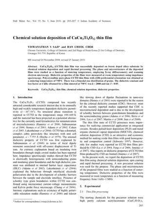
The variation of k and the dielectric loss recorded for the
films as a function of frequency of measurement is shown
in figure 4. The dielectric measurements were carried out
in four selected frequencies, viz. 1 kHz, 100 kHz,
500 kHz and 1 MHz. The CCTO film sintered at 750°C
showed a k value of ~ 2100 and a loss tangent of ~ 0⋅06 at
1 kHz. The decrease in k when sintering temperature was
above 900°C is associated with the trapped porosity as
observed by SEM. At higher measuring frequencies, k
decreased gradually, accompanied by a corresponding
increase in loss factor.
The large k at lower frequencies is suggested to be
associated with the Maxwell-Wagner contributions of
4. Viswanathan S Saji and Han Cheol Choe206
Figure 4. Dielectric constant and dielectric loss of CCTO thin film at different sintering temperatures
as a function of measuring frequency.
depletion layers at grain boundaries or interfaces between
the sample and contacts (Adams et al 2002; Lukenheimer
et al 2004). So far, the internal barrier layer capacitor
(IBLC) model has been widely accepted as the most
likely mechanism to elucidate the CDC in CCTO. The
difference of conductivity between grain boundary and
grain volume causes the charge accumulation on the grain
boundary on a mesoscopic scale, which results in large
quantity boundary barrier layer capacitors. On a macro-
scopic scale, the electrode contact effect may play a
significant role in CDC. Liu et al (2008) showed that
electrode and grain boundary act as two depletion layers
with distinct relaxation. On increasing the frequency, the
space charge polarization relaxes leading to decrease in k.
It has been shown that the frequency of dielectric relaxa-
tion was much lower in the case of CCTO film when
compared to that of the bulk ceramic (Shri Prakash et al
2008). The dielectric properties of the film obtained in
the present work is comparable with that reported for
polycrystalline CCTO thin films (Si et al 2002; Fang and
Shen 2003; Fang et al 2004; Shri Prakash et al 2008).
The high dielectric constant obtained for the CCTO film
in the present study indicates its possible application in
microelectronic devices.
4. Conclusions
Highly oriented CCTO thin films were successfully
deposited on boron doped silica substrate at a sintering
temperature of 750°C. Effect of sintering temperature on
the phase and microstructure of the film was investigated.
The film formed was polycrystalline in nature with (220)
preferential orientation. SEM microstructures of the films
revealed a bimodal size distribution of grains. Dielectric
constant and loss tangent at 1 kHz obtained for the film
sintered at 750°C was k ~ 2000 and tanδ ~ 0⋅05, respec-
tively.
Acknowledgement
The authors express their sincere gratitude to Professor
Yong Soo Cho, Department of Materials Science and
Engineering, Yonsei University, Korea.
5. Chemical solution deposition of CaCu3Ti4O12 thin film 207
References
Adams T B, Sinclair D C and West A R 2002 Adv. Mater. 14
1321
Adams T B, Sinclair D C and West A R 2006 Phys. Rev. B73
094124
Bochu B, Deschizeaux M N and Joubert J C 1979 J. Solid State
Chem. 29 291
Briźe V, Gruener G, Wolfman J, Fstyeyeva K, Tabellout M and
Gervais F 2006 Mater. Sci. Eng. B129 135
Chung S Y, Kim I L and Kang S J L 2004 Nat. Mater. 3 774
Cohen M H, Neaton J B, He L and Vanderbilt D 2003 J. Appl.
Phys. 94 3299
Fang L and Shen M 2003 Thin Solid Films 440 60
Fang L, Shen M and Cao W 2004 J. Appl. Phys. 95 6483
Feng L, Wang Y, Yan Y, Cao G and Jiao Z 2006 Appl. Surf.
Sci. 253 2268
Homes C C, Vogt T, Shapiro S M, Wakimoto S and Ramirez
A P 2001 Science 293 673
Jiménez R, Calzada M L, Bretos I, Goes J C and Sombra A S B
2007 J. Eur. Ceram. Soc. 27 3829
Leret P, Fernandez J F, de Frutos J and Fernandez-Hevia D
2007 J. Eur. Ceram. Soc. 27 3901
Liu L, Fan H, Fang P and Jin L 2007 Solid State Commun. 142
573
Liu L, Fan H, Wang L, Chen X and Fang P 2008 Philos. Mag.
88 537
Lu W, Feng L, Cao G and Jiao Z 2004 J. Mater. Sci. 39 3523
Lukenheimer P, Fichtl R, Ebbinghaus S G and Loidl A 2004
Phys. Rev. B70 172102.
Martin L, Guillemet-Fritsch S, Durand B, Levchenko A A,
Navrotsky A and Lebey T 2008 J. Am. Ceram. Soc. 91 485
Ramirez A P, Subramanian M A, Gardel M G, Blumberg G, Li
D, Vogt T and Shapiro S M 2000 Solid State Commun. 115 217
Schwartz R W 1997 Chem. Mater. 9 2325
Shri Prakash B, Varma K B R, Michau D and Maglione M 2008
Thin Solid Films 516 2874
Si W, Cruz E M, Johnson P D, Barnes P W, Woodward P and
Ramirez A P 2002 Appl. Phys. Lett. 81 2056
Subramanian M A, Li D, Duan N, Reisner B A and Sleight A W
2000 J. Solid State Chem. 151 323
Sun D L, Wu A Y and Yin S T 2008 J. Am. Ceram. Soc. 91 169