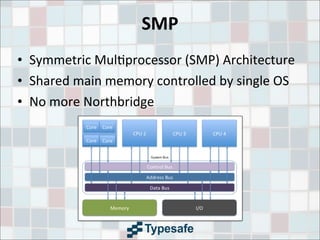
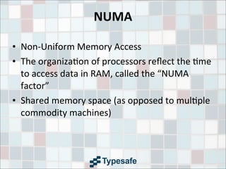
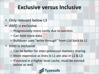
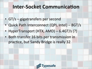
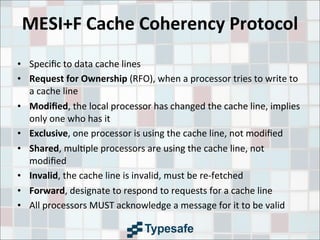
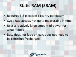
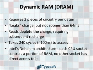
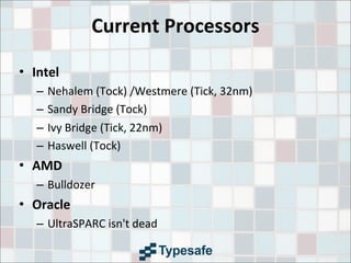
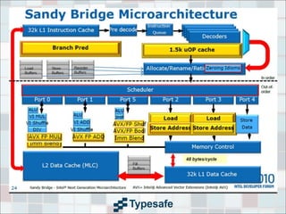
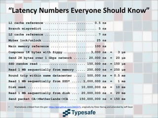
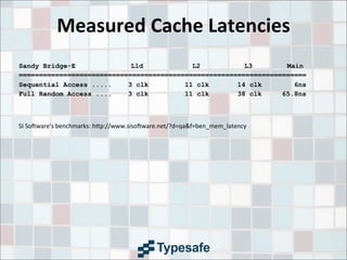
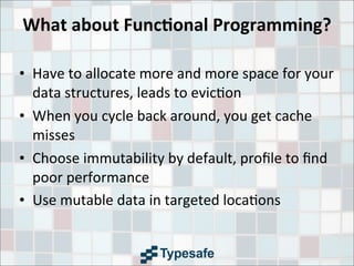
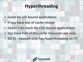
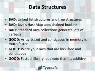
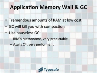
CPU	
  Caches
Jamie	
  Allen
Director	
  of	
  Consul3ng
@jamie_allen
h9p://github.com/jamie-­‐allen
Agenda
• Goal
• Defini3ons
• Architectures
• Development	
  Tips
• The	
  Future
Goal
Provide	
  you	
  with	
  the	
  informa3on	
  you	
  need	
  
about	
  CPU	
  caches	
  so	
  that	
  you	
  can	
  improve	
  the	
  
performance	
  of	
  your	
  applica3ons
Why?
• Increased	
  virtualiza3on	
  
– Run3me	
  (JVM,	
  RVM)
– PlaRorms/Environments	
  (cloud)
• Disruptor,	
  2011
Deni7ons
SMP
• Symmetric	
  Mul3processor	
  (SMP)	
  Architecture
• Shared	
  main	
  memory	
  controlled	
  by	
  single	
  OS
• No	
  more	
  Northbridge
NUMA
• Non-­‐Uniform	
  Memory	
  Access
• The	
  organiza3on	
  of	
  processors	
  reflect	
  the	
  3me	
  
to	
  access	
  data	
  in	
  RAM,	
  called	
  the	
  “NUMA	
  
factor”
• Shared	
  memory	
  space	
  (as	
  opposed	
  to	
  mul3ple	
  
commodity	
  machines)
Data	
  Locality
• The	
  most	
  cri3cal	
  factor	
  in	
  performance?	
  	
  
Google	
  argues	
  otherwise!
• Not	
  guaranteed	
  by	
  a	
  JVM
• Spa7al	
  -­‐	
  reused	
  over	
  and	
  over	
  in	
  a	
  loop,	
  data	
  
accessed	
  in	
  small	
  regions
• Temporal	
  -­‐	
  high	
  probability	
  it	
  will	
  be	
  reused	
  
before	
  long
Memory	
  Controller
• Manages	
  communica3on	
  of	
  reads/writes	
  
between	
  the	
  CPU	
  and	
  RAM
• Integrated	
  Memory	
  Controller	
  on	
  die
Cache	
  Lines
• 32-­‐256	
  con3guous	
  bytes,	
  most	
  commonly	
  64
• Beware	
  “false	
  sharing”
• Use	
  padding	
  to	
  ensure	
  unshared	
  lines
• Transferred	
  in	
  64-­‐bit	
  blocks	
  (8x	
  for	
  64	
  byte	
  
lines),	
  arriving	
  every	
  ~4	
  cycles
• Posi3on	
  in	
  the	
  line	
  of	
  the	
  “cri3cal	
  word”	
  
ma9ers,	
  but	
  not	
  if	
  pre-­‐fetched
• @Contended	
  annota3on	
  coming	
  in	
  Java	
  8!
Cache	
  Associa7vity
• Fully	
  Associa7ve:	
  Put	
  it	
  anywhere
• Somewhere	
  in	
  the	
  middle:	
  n-­‐way	
  set-­‐
associa3ve,	
  2-­‐way	
  skewed-­‐associa3ve
• Direct	
  Mapped:	
  Each	
  entry	
  can	
  only	
  go	
  in	
  one	
  
specic	
  place	
  
Cache	
  Evic7on	
  Strategies
• Least	
  Recently	
  Used	
  (LRU)
• Pseudo-­‐LRU	
  (PLRU):	
  for	
  large	
  associa3vity	
  
caches
• 2-­‐Way	
  Set	
  Associa7ve
• Direct	
  Mapped
• Others
Cache	
  Write	
  Strategies
• Write	
  through:	
  changed	
  cache	
  line	
  
immediately	
  goes	
  back	
  to	
  main	
  memory
• Write	
  back:	
  cache	
  line	
  is	
  marked	
  when	
  dirty,	
  
evic3on	
  sends	
  back	
  to	
  main	
  memory
• Write	
  combining:	
  grouped	
  writes	
  of	
  cache	
  
lines	
  back	
  to	
  main	
  memory
• Uncacheable:	
  dynamic	
  values	
  that	
  can	
  change	
  
without	
  warning
Exclusive	
  versus	
  Inclusive
• Only	
  relevant	
  below	
  L3
• AMD	
  is	
  exclusive
– Progressively	
  more	
  costly	
  due	
  to	
  evic3on
– Can	
  hold	
  more	
  data
– Bulldozer	
  uses	
  "write	
  through"	
  from	
  L1d	
  back	
  to	
  L2
• Intel	
  is	
  inclusive
– Can	
  be	
  be9er	
  for	
  inter-­‐processor	
  memory	
  sharing
– More	
  expensive	
  as	
  lines	
  in	
  L1	
  are	
  also	
  in	
  L2	
  &	
  L3
– If	
  evicted	
  in	
  a	
  higher	
  level	
  cache,	
  must	
  be	
  evicted	
  
below	
  as	
  well
Inter-­‐Socket	
  Communica7on
• GT/s	
  –	
  gigatransfers	
  per	
  second
• Quick	
  Path	
  Interconnect	
  (QPI,	
  Intel)	
  –	
  8GT/s
• HyperTransport	
  (HTX,	
  AMD)	
  –	
  6.4GT/s	
  (?)
• Both	
  transfer	
  16	
  bits	
  per	
  transmission	
  in	
  
prac3ce,	
  but	
  Sandy	
  Bridge	
  is	
  really	
  32
MESI+F	
  Cache	
  Coherency	
  Protocol
• Specific	
  to	
  data	
  cache	
  lines
• Request	
  for	
  Ownership	
  (RFO),	
  when	
  a	
  processor	
  tries	
  to	
  write	
  to	
  
a	
  cache	
  line
• Modified,	
  the	
  local	
  processor	
  has	
  changed	
  the	
  cache	
  line,	
  implies	
  
only	
  one	
  who	
  has	
  it
• Exclusive,	
  one	
  processor	
  is	
  using	
  the	
  cache	
  line,	
  not	
  modied
• Shared,	
  mul3ple	
  processors	
  are	
  using	
  the	
  cache	
  line,	
  not	
  
modied
• Invalid,	
  the	
  cache	
  line	
  is	
  invalid,	
  must	
  be	
  re-­‐fetched
• Forward,	
  designate	
  to	
  respond	
  to	
  requests	
  for	
  a	
  cache	
  line
• All	
  processors	
  MUST	
  acknowledge	
  a	
  message	
  for	
  it	
  to	
  be	
  valid
Sta7c	
  RAM	
  (SRAM)
• Requires	
  6-­‐8	
  pieces	
  of	
  circuitry	
  per	
  datum
• Cycle	
  rate	
  access,	
  not	
  quite	
  measurable	
  in	
  3me
• Uses	
  a	
  rela3vely	
  large	
  amount	
  of	
  power	
  for	
  
what	
  it	
  does
• Data	
  does	
  not	
  fade	
  or	
  leak,	
  does	
  not	
  need	
  to	
  
be	
  refreshed/recharged
Dynamic	
  RAM	
  (DRAM)
• Requires	
  2	
  pieces	
  of	
  circuitry	
  per	
  datum
• “Leaks”	
  charge,	
  but	
  not	
  sooner	
  than	
  64ms
• Reads	
  deplete	
  the	
  charge,	
  requiring	
  
subsequent	
  recharge
• Takes	
  240	
  cycles	
  (~100ns)	
  to	
  access
• Intel's	
  Nehalem	
  architecture	
  -­‐	
  each	
  CPU	
  socket	
  
controls	
  a	
  por3on	
  of	
  RAM,	
  no	
  other	
  socket	
  has	
  
direct	
  access	
  to	
  it
Architectures
Current	
  Processors
• Intel
– Nehalem	
  (Tock)	
  /Westmere	
  (Tick,	
  32nm)
– Sandy	
  Bridge	
  (Tock)
– Ivy	
  Bridge	
  (Tick,	
  22nm)
– Haswell	
  (Tock)
• AMD
– Bulldozer
• Oracle
– UltraSPARC	
  isn't	
  dead
“Latency	
  Numbers	
  Everyone	
  Should	
  Know”
L1 cache reference ......................... 0.5 ns
Branch mispredict ............................ 5 ns
L2 cache reference ........................... 7 ns
Mutex lock/unlock ........................... 25 ns
Main memory reference ...................... 100 ns
Compress 1K bytes with Zippy ............. 3,000 ns = 3 Âľs
Send 2K bytes over 1 Gbps network ....... 20,000 ns = 20 Âľs
SSD random read ........................ 150,000 ns = 150 Âľs
Read 1 MB sequentially from memory ..... 250,000 ns = 250 Âľs
Round trip within same datacenter ...... 500,000 ns = 0.5 ms
Read 1 MB sequentially from SSD* ..... 1,000,000 ns = 1 ms
Disk seek ........................... 10,000,000 ns = 10 ms
Read 1 MB sequentially from disk .... 20,000,000 ns = 20 ms
Send packet CA->Netherlands->CA .... 150,000,000 ns = 150 ms
• Shamelessly	
  cribbed	
  from	
  this	
  gist:	
  h9ps://gist.github.com/2843375,	
  originally	
  by	
  Peter	
  Norvig	
  and	
  amended	
  by	
  Jeff	
  Dean
Measured	
  Cache	
  Latencies
Sandy Bridge-E L1d L2 L3 Main
=======================================================================
Sequential Access ..... 3 clk 11 clk 14 clk 6ns
Full Random Access .... 3 clk 11 clk 38 clk 65.8ns
SI	
  Sotware's	
  benchmarks:	
  h9p://www.sisotware.net/?d=qa&f=ben_mem_latency
Registers
• On-­‐core	
  for	
  instruc3ons	
  being	
  executed	
  and	
  
their	
  operands
• Can	
  be	
  accessed	
  in	
  a	
  single	
  cycle
• There	
  are	
  many	
  different	
  types
• A	
  64-­‐bit	
  Intel	
  Nehalem	
  CPU	
  had	
  128	
  Integer	
  &	
  
128	
  floa3ng	
  point	
  registers
Store	
  Buffers
• Hold	
  data	
  for	
  Out	
  of	
  Order	
  (OoO)	
  execu3on
• Fully	
  associa3ve
• Prevent	
  “stalls”	
  in	
  execu3on	
  on	
  a	
  thread	
  when	
  
the	
  cache	
  line	
  is	
  not	
  local	
  to	
  a	
  core	
  on	
  a	
  write
• ~1	
  cycle
Level	
  Zero	
  (L0)
• Added	
  in	
  Sandy	
  Bridge
• A	
  cache	
  of	
  the	
  last	
  1536	
  uops	
  decoded
• Well-­‐suited	
  for	
  hot	
  loops
• Not	
  the	
  same	
  as	
  the	
  older	
  "trace"	
  cache
Level	
  One	
  (L1)
• Divided	
  into	
  data	
  and	
  instruc3ons
• 32K	
  data	
  (L1d),	
  32K	
  instruc3ons	
  (L1i)	
  per	
  core	
  
on	
  a	
  Sandy	
  Bridge,	
  Ivy	
  Bridge	
  and	
  Haswell
• Sandy	
  Bridge	
  loads	
  data	
  at	
  256	
  bits	
  per	
  cycle,	
  
double	
  that	
  of	
  Nehalem
• 3-­‐4	
  cycles	
  to	
  access	
  L1d
Level	
  Two	
  (L2)
• 256K	
  per	
  core	
  on	
  a	
  Sandy	
  Bridge,	
  Ivy	
  Bridge	
  &	
  
Haswell
• 2MB	
  per	
  “module”	
  on	
  AMD's	
  Bulldozer	
  
architecture
• ~11	
  cycles	
  to	
  access
• Unified	
  data	
  and	
  instruc3on	
  caches	
  from	
  here	
  
up
• If	
  the	
  working	
  set	
  size	
  is	
  larger	
  than	
  L2,	
  misses	
  
grow
Level	
  Three	
  (L3)
• Was	
  a	
  “unified”	
  cache	
  up	
  un3l	
  Sandy	
  Bridge,	
  
shared	
  between	
  cores
• Varies	
  in	
  size	
  with	
  different	
  processors	
  and	
  
versions	
  of	
  an	
  architecture.	
  	
  Laptops	
  might	
  
have	
  6-­‐8MB,	
  but	
  server-­‐class	
  might	
  have	
  
30MB.
• 14-­‐38	
  cycles	
  to	
  access
Level	
  Four???	
  (L4)
• Some	
  versions	
  of	
  Haswell	
  will	
  have	
  a	
  128	
  MB	
  
L4	
  cache!
• No	
  latency	
  benchmarks	
  for	
  this	
  yet
Programming	
  Tips
Striding	
  &	
  Pre-­‐fetching
• Predictable	
  memory	
  access	
  is	
  really	
  important
• Hardware	
  pre-­‐fetcher	
  on	
  the	
  core	
  looks	
  for	
  
pa9erns	
  of	
  memory	
  access
• Can	
  be	
  counter-­‐produc3ve	
  if	
  the	
  access	
  
pa9ern	
  is	
  not	
  predictable
• Mar3n	
  Thompson	
  blog	
  post:	
  “Memory	
  Access	
  
Pa9erns	
  are	
  Important”
• Shows	
  the	
  importance	
  of	
  locality	
  and	
  striding
Cache	
  Misses
• Cost	
  hundreds	
  of	
  cycles
• Keep	
  your	
  code	
  simple
• Instruc3on	
  read	
  misses	
  are	
  most	
  expensive
• Data	
  read	
  miss	
  are	
  less	
  so,	
  but	
  s3ll	
  hurt	
  performance
• Write	
  misses	
  are	
  okay	
  unless	
  using	
  Write	
  Through
• Miss	
  types:
– Compulsory
– Capacity
– Conflict
Programming	
  Op7miza7ons
• Stack	
  allocated	
  data	
  is	
  cheap
• Pointer	
  interac3on	
  -­‐	
  you	
  have	
  to	
  retrieve	
  data	
  
being	
  pointed	
  to,	
  even	
  in	
  registers
• Avoid	
  locking	
  and	
  resultant	
  kernel	
  arbitra3on
• CAS	
  is	
  be9er	
  and	
  occurs	
  on-­‐thread,	
  but	
  
algorithms	
  become	
  more	
  complex
• Match	
  workload	
  to	
  the	
  size	
  of	
  the	
  last	
  level	
  
cache	
  (LLC,	
  L3/L4)
What	
  about	
  Func7onal	
  Programming?
• Have	
  to	
  allocate	
  more	
  and	
  more	
  space	
  for	
  your	
  
data	
  structures,	
  leads	
  to	
  evic3on
• When	
  you	
  cycle	
  back	
  around,	
  you	
  get	
  cache	
  
misses
• Choose	
  immutability	
  by	
  default,	
  prole	
  to	
  nd	
  
poor	
  performance
• Use	
  mutable	
  data	
  in	
  targeted	
  loca3ons
Hyperthreading
• Great	
  for	
  I/O-­‐bound	
  applica3ons
• If	
  you	
  have	
  lots	
  of	
  cache	
  misses
• Doesn't	
  do	
  much	
  for	
  CPU-­‐bound	
  applica3ons
• You	
  have	
  half	
  of	
  the	
  cache	
  resources	
  per	
  core
• NOTE	
  -­‐	
  Haswell	
  only	
  has	
  Hyperthreading	
  on	
  i7!
Data	
  Structures
• BAD:	
  Linked	
  list	
  structures	
  and	
  tree	
  structures
• BAD:	
  Java's	
  HashMap	
  uses	
  chained	
  buckets
• BAD:	
  Standard	
  Java	
  collec3ons	
  generate	
  lots	
  of	
  
garbage
• GOOD:	
  Array-­‐based	
  and	
  con3guous	
  in	
  memory	
  is	
  
much	
  faster
• GOOD:	
  Write	
  your	
  own	
  that	
  are	
  lock-­‐free	
  and	
  
con3guous
• GOOD:	
  Fastu3l	
  library,	
  but	
  note	
  that	
  it's	
  addi3ve
Applica7on	
  Memory	
  Wall	
  &	
  GC
• Tremendous	
  amounts	
  of	
  RAM	
  at	
  low	
  cost
• GC	
  will	
  kill	
  you	
  with	
  compac3on
• Use	
  pauseless	
  GC
– IBM's	
  Metronome,	
  very	
  predictable
– Azul's	
  C4,	
  very	
  performant
Using	
  GPUs
• Remember,	
  locality	
  ma9ers!
• Need	
  to	
  be	
  able	
  to	
  export	
  a	
  task	
  with	
  data	
  that	
  
does	
  not	
  need	
  to	
  update
• AMD	
  has	
  the	
  new	
  HSA	
  plaRorm	
  which	
  
communicates	
  between	
  GPUs	
  and	
  CPUs	
  via	
  
shared	
  L3
The	
  Future
ManyCore
• David	
  Ungar	
  says	
  >	
  24	
  cores,	
  generally	
  many	
  
10s	
  of	
  cores
• Really	
  gets	
  interes3ng	
  above	
  1000	
  cores
• Cache	
  coherency	
  won't	
  be	
  possible
• Non-­‐determinis3c
Memristor
• Non-­‐vola3le,	
  sta3c	
  RAM,	
  same	
  write	
  
endurance	
  as	
  Flash
• 200-­‐300	
  MB	
  on	
  chip
• Sub-­‐nanosecond	
  writes
• Able	
  to	
  perform	
  processing?	
  	
  (Probably	
  not)
• Mul3state,	
  not	
  binary
Phase	
  Change	
  Memory	
  (PRAM)
• Higher	
  performance	
  than	
  today's	
  DRAM
• Intel	
  seems	
  more	
  fascinated	
  by	
  this,	
  released	
  
its	
  "neuromorphic"	
  chip	
  design	
  last	
  Fall
• Not	
  able	
  to	
  perform	
  processing
• Write	
  degrada3on	
  is	
  supposedly	
  much	
  slower
• Was	
  considered	
  suscep3ble	
  to	
  uninten3onal	
  
change,	
  maybe	
  xed?
Thanks!
Credits!
• What	
  Every	
  Programmer	
  Should	
  Know	
  About	
  Memory,	
  Ulrich	
  Drepper	
  of	
  
RedHat,	
  2007
• Java	
  Performance,	
  Charlie	
  Hunt
• Wikipedia/Wikimedia	
  Commons
• AnandTech
• The	
  Microarchitecture	
  of	
  AMD,	
  Intel	
  and	
  VIA	
  CPUs
• Everything	
  You	
  Need	
  to	
  Know	
  about	
  the	
  Quick	
  Path	
  Interconnect,	
  Gabriel	
  
Torres/Hardware	
  Secrets
• Inside	
  the	
  Sandy	
  Bridge	
  Architecture,	
  Gabriel	
  Torres/Hardware	
  Secrets
• Mar3n	
  Thompson's	
  Mechanical	
  Sympathy	
  blog	
  and	
  Disruptor	
  presenta3ons
• The	
  Applica3on	
  Memory	
  Wall,	
  Gil	
  Tene,	
  CTO	
  of	
  Azul	
  Systems
• AMD	
  Bulldozer/Intel	
  Sandy	
  Bridge	
  Comparison,	
  Gionatan	
  Dan3
• SI	
  Sotware's	
  Memory	
  Latency	
  Benchmarks
• Mar3n	
  Thompson	
  and	
  Cliff	
  Click	
  provided	
  feedback	
  &addi3onal	
  content

Cpu Caches

  • 1.
    CPU  Caches Jamie  Allen Director  of  Consul3ng @jamie_allen h9p://github.com/jamie-­‐allen
  • 2.
    Agenda • Goal • Defini3ons •Architectures • Development  Tips • The  Future
  • 3.
    Goal Provide  you  with  the  informa3on  you  need   about  CPU  caches  so  that  you  can  improve  the   performance  of  your  applica3ons
  • 4.
    Why? • Increased  virtualiza3on   – Run3me  (JVM,  RVM) – PlaRorms/Environments  (cloud) • Disruptor,  2011
  • 5.
  • 6.
    SMP • Symmetric  Mul3processor  (SMP)  Architecture • Shared  main  memory  controlled  by  single  OS • No  more  Northbridge
  • 7.
    NUMA • Non-­‐Uniform  Memory  Access • The  organiza3on  of  processors  reflect  the  3me   to  access  data  in  RAM,  called  the  “NUMA   factor” • Shared  memory  space  (as  opposed  to  mul3ple   commodity  machines)
  • 8.
    Data  Locality • The  most  cri3cal  factor  in  performance?     Google  argues  otherwise! • Not  guaranteed  by  a  JVM • Spa7al  -­‐  reused  over  and  over  in  a  loop,  data   accessed  in  small  regions • Temporal  -­‐  high  probability  it  will  be  reused   before  long
  • 9.
    Memory  Controller • Manages  communica3on  of  reads/writes   between  the  CPU  and  RAM • Integrated  Memory  Controller  on  die
  • 10.
    Cache  Lines • 32-­‐256  con3guous  bytes,  most  commonly  64 • Beware  “false  sharing” • Use  padding  to  ensure  unshared  lines • Transferred  in  64-­‐bit  blocks  (8x  for  64  byte   lines),  arriving  every  ~4  cycles • Posi3on  in  the  line  of  the  “cri3cal  word”   ma9ers,  but  not  if  pre-­‐fetched • @Contended  annota3on  coming  in  Java  8!
  • 11.
    Cache  Associa7vity • Fully  Associa7ve:  Put  it  anywhere • Somewhere  in  the  middle:  n-­‐way  set-­‐ associa3ve,  2-­‐way  skewed-­‐associa3ve • Direct  Mapped:  Each  entry  can  only  go  in  one   specific  place  
  • 12.
    Cache  Evic7on  Strategies •Least  Recently  Used  (LRU) • Pseudo-­‐LRU  (PLRU):  for  large  associa3vity   caches • 2-­‐Way  Set  Associa7ve • Direct  Mapped • Others
  • 13.
    Cache  Write  Strategies •Write  through:  changed  cache  line   immediately  goes  back  to  main  memory • Write  back:  cache  line  is  marked  when  dirty,   evic3on  sends  back  to  main  memory • Write  combining:  grouped  writes  of  cache   lines  back  to  main  memory • Uncacheable:  dynamic  values  that  can  change   without  warning
  • 14.
    Exclusive  versus  Inclusive •Only  relevant  below  L3 • AMD  is  exclusive – Progressively  more  costly  due  to  evic3on – Can  hold  more  data – Bulldozer  uses  "write  through"  from  L1d  back  to  L2 • Intel  is  inclusive – Can  be  be9er  for  inter-­‐processor  memory  sharing – More  expensive  as  lines  in  L1  are  also  in  L2  &  L3 – If  evicted  in  a  higher  level  cache,  must  be  evicted   below  as  well
  • 15.
    Inter-­‐Socket  Communica7on • GT/s  –  gigatransfers  per  second • Quick  Path  Interconnect  (QPI,  Intel)  –  8GT/s • HyperTransport  (HTX,  AMD)  –  6.4GT/s  (?) • Both  transfer  16  bits  per  transmission  in   prac3ce,  but  Sandy  Bridge  is  really  32
  • 16.
    MESI+F  Cache  Coherency  Protocol • Specific  to  data  cache  lines • Request  for  Ownership  (RFO),  when  a  processor  tries  to  write  to   a  cache  line • Modified,  the  local  processor  has  changed  the  cache  line,  implies   only  one  who  has  it • Exclusive,  one  processor  is  using  the  cache  line,  not  modified • Shared,  mul3ple  processors  are  using  the  cache  line,  not   modified • Invalid,  the  cache  line  is  invalid,  must  be  re-­‐fetched • Forward,  designate  to  respond  to  requests  for  a  cache  line • All  processors  MUST  acknowledge  a  message  for  it  to  be  valid
  • 17.
    Sta7c  RAM  (SRAM) •Requires  6-­‐8  pieces  of  circuitry  per  datum • Cycle  rate  access,  not  quite  measurable  in  3me • Uses  a  rela3vely  large  amount  of  power  for   what  it  does • Data  does  not  fade  or  leak,  does  not  need  to   be  refreshed/recharged
  • 18.
    Dynamic  RAM  (DRAM) •Requires  2  pieces  of  circuitry  per  datum • “Leaks”  charge,  but  not  sooner  than  64ms • Reads  deplete  the  charge,  requiring   subsequent  recharge • Takes  240  cycles  (~100ns)  to  access • Intel's  Nehalem  architecture  -­‐  each  CPU  socket   controls  a  por3on  of  RAM,  no  other  socket  has   direct  access  to  it
  • 19.
  • 20.
    Current  Processors • Intel –Nehalem  (Tock)  /Westmere  (Tick,  32nm) – Sandy  Bridge  (Tock) – Ivy  Bridge  (Tick,  22nm) – Haswell  (Tock) • AMD – Bulldozer • Oracle – UltraSPARC  isn't  dead
  • 22.
    “Latency  Numbers  Everyone  Should  Know” L1 cache reference ......................... 0.5 ns Branch mispredict ............................ 5 ns L2 cache reference ........................... 7 ns Mutex lock/unlock ........................... 25 ns Main memory reference ...................... 100 ns Compress 1K bytes with Zippy ............. 3,000 ns = 3 µs Send 2K bytes over 1 Gbps network ....... 20,000 ns = 20 µs SSD random read ........................ 150,000 ns = 150 µs Read 1 MB sequentially from memory ..... 250,000 ns = 250 µs Round trip within same datacenter ...... 500,000 ns = 0.5 ms Read 1 MB sequentially from SSD* ..... 1,000,000 ns = 1 ms Disk seek ........................... 10,000,000 ns = 10 ms Read 1 MB sequentially from disk .... 20,000,000 ns = 20 ms Send packet CA->Netherlands->CA .... 150,000,000 ns = 150 ms • Shamelessly  cribbed  from  this  gist:  h9ps://gist.github.com/2843375,  originally  by  Peter  Norvig  and  amended  by  Jeff  Dean
  • 23.
    Measured  Cache  Latencies SandyBridge-E L1d L2 L3 Main ======================================================================= Sequential Access ..... 3 clk 11 clk 14 clk 6ns Full Random Access .... 3 clk 11 clk 38 clk 65.8ns SI  Sotware's  benchmarks:  h9p://www.sisotware.net/?d=qa&f=ben_mem_latency
  • 24.
    Registers • On-­‐core  for  instruc3ons  being  executed  and   their  operands • Can  be  accessed  in  a  single  cycle • There  are  many  different  types • A  64-­‐bit  Intel  Nehalem  CPU  had  128  Integer  &   128  floa3ng  point  registers
  • 25.
    Store  Buffers • Hold  data  for  Out  of  Order  (OoO)  execu3on • Fully  associa3ve • Prevent  “stalls”  in  execu3on  on  a  thread  when   the  cache  line  is  not  local  to  a  core  on  a  write • ~1  cycle
  • 26.
    Level  Zero  (L0) •Added  in  Sandy  Bridge • A  cache  of  the  last  1536  uops  decoded • Well-­‐suited  for  hot  loops • Not  the  same  as  the  older  "trace"  cache
  • 27.
    Level  One  (L1) •Divided  into  data  and  instruc3ons • 32K  data  (L1d),  32K  instruc3ons  (L1i)  per  core   on  a  Sandy  Bridge,  Ivy  Bridge  and  Haswell • Sandy  Bridge  loads  data  at  256  bits  per  cycle,   double  that  of  Nehalem • 3-­‐4  cycles  to  access  L1d
  • 28.
    Level  Two  (L2) •256K  per  core  on  a  Sandy  Bridge,  Ivy  Bridge  &   Haswell • 2MB  per  “module”  on  AMD's  Bulldozer   architecture • ~11  cycles  to  access • Unified  data  and  instruc3on  caches  from  here   up • If  the  working  set  size  is  larger  than  L2,  misses   grow
  • 29.
    Level  Three  (L3) •Was  a  “unified”  cache  up  un3l  Sandy  Bridge,   shared  between  cores • Varies  in  size  with  different  processors  and   versions  of  an  architecture.    Laptops  might   have  6-­‐8MB,  but  server-­‐class  might  have   30MB. • 14-­‐38  cycles  to  access
  • 30.
    Level  Four???  (L4) •Some  versions  of  Haswell  will  have  a  128  MB   L4  cache! • No  latency  benchmarks  for  this  yet
  • 31.
  • 32.
    Striding  &  Pre-­‐fetching •Predictable  memory  access  is  really  important • Hardware  pre-­‐fetcher  on  the  core  looks  for   pa9erns  of  memory  access • Can  be  counter-­‐produc3ve  if  the  access   pa9ern  is  not  predictable • Mar3n  Thompson  blog  post:  “Memory  Access   Pa9erns  are  Important” • Shows  the  importance  of  locality  and  striding
  • 33.
    Cache  Misses • Cost  hundreds  of  cycles • Keep  your  code  simple • Instruc3on  read  misses  are  most  expensive • Data  read  miss  are  less  so,  but  s3ll  hurt  performance • Write  misses  are  okay  unless  using  Write  Through • Miss  types: – Compulsory – Capacity – Conflict
  • 34.
    Programming  Op7miza7ons • Stack  allocated  data  is  cheap • Pointer  interac3on  -­‐  you  have  to  retrieve  data   being  pointed  to,  even  in  registers • Avoid  locking  and  resultant  kernel  arbitra3on • CAS  is  be9er  and  occurs  on-­‐thread,  but   algorithms  become  more  complex • Match  workload  to  the  size  of  the  last  level   cache  (LLC,  L3/L4)
  • 35.
    What  about  Func7onal  Programming? • Have  to  allocate  more  and  more  space  for  your   data  structures,  leads  to  evic3on • When  you  cycle  back  around,  you  get  cache   misses • Choose  immutability  by  default,  profile  to  find   poor  performance • Use  mutable  data  in  targeted  loca3ons
  • 36.
    Hyperthreading • Great  for  I/O-­‐bound  applica3ons • If  you  have  lots  of  cache  misses • Doesn't  do  much  for  CPU-­‐bound  applica3ons • You  have  half  of  the  cache  resources  per  core • NOTE  -­‐  Haswell  only  has  Hyperthreading  on  i7!
  • 37.
    Data  Structures • BAD:  Linked  list  structures  and  tree  structures • BAD:  Java's  HashMap  uses  chained  buckets • BAD:  Standard  Java  collec3ons  generate  lots  of   garbage • GOOD:  Array-­‐based  and  con3guous  in  memory  is   much  faster • GOOD:  Write  your  own  that  are  lock-­‐free  and   con3guous • GOOD:  Fastu3l  library,  but  note  that  it's  addi3ve
  • 38.
    Applica7on  Memory  Wall  &  GC • Tremendous  amounts  of  RAM  at  low  cost • GC  will  kill  you  with  compac3on • Use  pauseless  GC – IBM's  Metronome,  very  predictable – Azul's  C4,  very  performant
  • 39.
    Using  GPUs • Remember,  locality  ma9ers! • Need  to  be  able  to  export  a  task  with  data  that   does  not  need  to  update • AMD  has  the  new  HSA  plaRorm  which   communicates  between  GPUs  and  CPUs  via   shared  L3
  • 40.
  • 41.
    ManyCore • David  Ungar  says  >  24  cores,  generally  many   10s  of  cores • Really  gets  interes3ng  above  1000  cores • Cache  coherency  won't  be  possible • Non-­‐determinis3c
  • 42.
    Memristor • Non-­‐vola3le,  sta3c  RAM,  same  write   endurance  as  Flash • 200-­‐300  MB  on  chip • Sub-­‐nanosecond  writes • Able  to  perform  processing?    (Probably  not) • Mul3state,  not  binary
  • 43.
    Phase  Change  Memory  (PRAM) • Higher  performance  than  today's  DRAM • Intel  seems  more  fascinated  by  this,  released   its  "neuromorphic"  chip  design  last  Fall • Not  able  to  perform  processing • Write  degrada3on  is  supposedly  much  slower • Was  considered  suscep3ble  to  uninten3onal   change,  maybe  fixed?
  • 44.
  • 45.
    Credits! • What  Every  Programmer  Should  Know  About  Memory,  Ulrich  Drepper  of   RedHat,  2007 • Java  Performance,  Charlie  Hunt • Wikipedia/Wikimedia  Commons • AnandTech • The  Microarchitecture  of  AMD,  Intel  and  VIA  CPUs • Everything  You  Need  to  Know  about  the  Quick  Path  Interconnect,  Gabriel   Torres/Hardware  Secrets • Inside  the  Sandy  Bridge  Architecture,  Gabriel  Torres/Hardware  Secrets • Mar3n  Thompson's  Mechanical  Sympathy  blog  and  Disruptor  presenta3ons • The  Applica3on  Memory  Wall,  Gil  Tene,  CTO  of  Azul  Systems • AMD  Bulldozer/Intel  Sandy  Bridge  Comparison,  Gionatan  Dan3 • SI  Sotware's  Memory  Latency  Benchmarks • Mar3n  Thompson  and  Cliff  Click  provided  feedback  &addi3onal  content