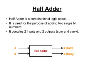
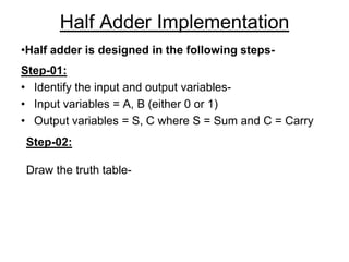
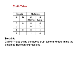
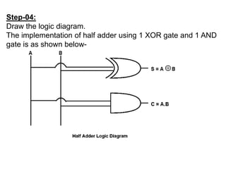
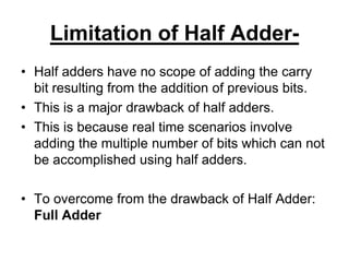
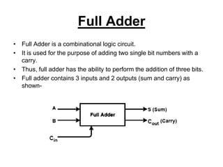
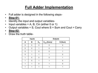
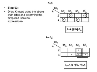
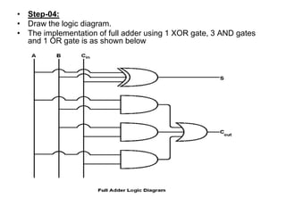
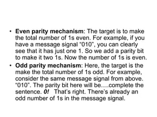
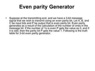
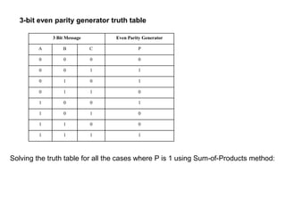
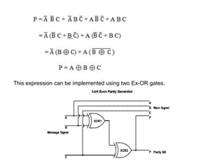
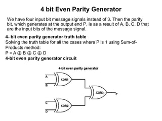
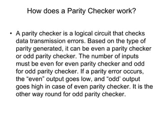
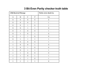
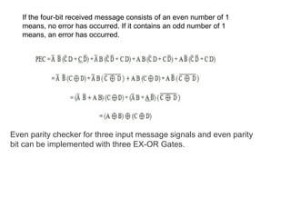
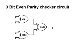
Module I
Digital Logic Design
Half Adder
• Half Adder is a combinational logic circuit.
• It is used for the purpose of adding two single bit
numbers.
• It contains 2 inputs and 2 outputs (sum and carry).
Half Adder Implementation
Step-01:
• Identify the input and output variables-
• Input variables = A, B (either 0 or 1)
• Output variables = S, C where S = Sum and C = Carry
•Half adder is designed in the following steps-
Step-02:
Draw the truth table-
Inputs Outputs
A B C
(Carry)
S
(Sum)
0 0 0 0
0 1 0 1
1 0 0 1
1 1 1 0
Truth Table
Step-03:
Draw K-maps using the above truth table and determine the
simplified Boolean expressions-
Step-04:
Draw the logic diagram.
The implementation of half adder using 1 XOR gate and 1 AND
gate is as shown below-
Limitation of Half Adder-
• Half adders have no scope of adding the carry
bit resulting from the addition of previous bits.
• This is a major drawback of half adders.
• This is because real time scenarios involve
adding the multiple number of bits which can not
be accomplished using half adders.
• To overcome from the drawback of Half Adder:
Full Adder
Full Adder
• Full Adder is a combinational logic circuit.
• It is used for the purpose of adding two single bit numbers with a
carry.
• Thus, full adder has the ability to perform the addition of three bits.
• Full adder contains 3 inputs and 2 outputs (sum and carry) as
shown-
Full Adder Implementation
• Full adder is designed in the following steps-
• Step-01:
• Identify the input and output variables-
• Input variables = A, B, Cin (either 0 or 1)
• Output variables = S, Cout where S = Sum and Cout = Carry
• Step-02:
• Draw the truth table-
Inputs Outputs
A B Cin Cout (Carry) S (Sum)
0 0 0 0 0
0 0 1 0 1
0 1 0 0 1
0 1 1 1 0
1 0 0 0 1
1 0 1 1 0
1 1 0 1 0
1 1 1 1 1
• Step-03:
• Draw K-maps using the above
truth table and determine the
simplified Boolean
expressions-
• Step-04:
• Draw the logic diagram.
• The implementation of full adder using 1 XOR gate, 3 AND gates
and 1 OR gate is as shown below
Parity Generator and Parity Checker
• In digital electronic systems, during data
transmission and processing, data gets
distorted. This is due to the noises added to it.
Such noises change 0s to 1s and 1s to 0s.
Annoying, right? It is necessary to identify and
remove these errors.
• One of the most widely used error detection
techniques for transmission of data for sharing
information between devices is Parity checking.
What is a Parity Bit?
• A parity bit is an extra bit in any binary message to make
the total number of 1’s either odd or even. We need to add
the parity bit to a signal. This is done by the Parity
generator. This parity inclusive binary message then
transmits from transmitter to receiver end.
• The Parity Checker matches the number of 1’s at the
receiver’s end with that of the transmitter’s end to check for
errors. If there is a change in the number of 1s at the
receiving end, then that detects the presence of an error.
What is even parity and odd parity?
Even parity is the case when the total number of 1s in
the sum of data bits and parity bits is even whereas, in
odd parity, it is odd.
• Even parity mechanism: The target is to make
the total number of 1s even. For example, if you
have a message signal “010”, you can clearly
see that it has just one 1. So we add a parity bit
to make it two 1s. Now the number of 1s is even.
• Odd parity mechanism: Here, the target is the
make the total number of 1s odd. For example,
consider the same message signal from above.
“010”. The parity bit here will be….complete the
sentence. 0! That’s right. There’s already an
odd number of 1s in the message signal.
Even parity Generator
• Suppose at the transmitting end, and we have a 3-bit message
signal that we wish to transmit using an even parity bit. Let A, B, and
C be input bits and P be output that is even parity bit. Even parity
generates as a result of the calculation of the number of ones in the
message bit. If the number of 1s is even P gets the value as 0, and if
it is odd, then the parity bit P gets the value 1. Following is the truth
table for 3-bit even parity generator.
3-bit even parity generator truth table
3 Bit Message Even Parity Generator
A B C P
0 0 0 0
0 0 1 1
0 1 0 1
0 1 1 0
1 0 0 1
1 0 1 0
1 1 0 0
1 1 1 1
Solving the truth table for all the cases where P is 1 using Sum-of-Products method:
This expression can be implemented using two Ex-OR gates.
4 bit Even Parity Generator
We have four input bit message signals instead of 3. Then the parity
bit, which generates at the output end P, is as a result of A, B, C, D that
are the input bits of the message signal.
4- bit even parity generator truth table
Solving the truth table for all the cases where P is 1 using Sum-of-
Products method:
P = A ⊕ B ⊕ C ⊕ D
4-bit even parity generator circuit
How does a Parity Checker work?
• A parity checker is a logical circuit that checks
data transmission errors. Based on the type of
parity generated, it can be even a parity checker
or odd parity checker. The number of inputs
must be even for even parity checker and odd
for odd parity checker. If a parity error occurs,
the “even” output goes low, and “odd’ output
goes high in case of even parity checker. It is the
other way round for odd parity checker.
Even Parity Checker
• 3 Bit Even Parity Checker
• Suppose at the transmitting end, even parity bit is generated, and
we have three input message signals and one parity bit. The parity
checker circuit is fed all these four bits to check for possible errors.
So a 3-bit parity checker actually has a 4-bit input.
• Since the transmitting end is working with even parity, the number of
1’s at received by the checker circuit must be even. For every case,
where the input to the parity checker has an odd number of 1s, the
error output will be 1.
• This high error output indicates that an error is present in the signal.
And for every input where the number of 1s is the expected even
count, the error output will be 0.
3 Bit Even Parity checker truth table
4 Bit Received Message Parity error check Cp
A B C P Cp
0 0 0 0 0
0 0 0 1 1
0 0 1 0 1
0 0 1 1 0
0 1 0 0 1
0 1 0 1 0
0 1 1 0 0
0 1 1 1 1
1 0 0 0 1
1 0 0 1 0
1 0 1 0 0
1 0 1 1 1
1 1 0 0 0
1 1 0 1 1
1 1 1 0 1
1 1 1 1 0
If the four-bit received message consists of an even number of 1
means, no error has occurred. If it contains an odd number of 1
means, an error has occurred.
Even parity checker for three input message signals and even parity
bit can be implemented with three EX-OR Gates.
3 Bit Even Parity checker circuit

Computer Organisation and Architecture :Module M-1.pdf

  • 1.
  • 2.
    Half Adder • HalfAdder is a combinational logic circuit. • It is used for the purpose of adding two single bit numbers. • It contains 2 inputs and 2 outputs (sum and carry).
  • 3.
    Half Adder Implementation Step-01: •Identify the input and output variables- • Input variables = A, B (either 0 or 1) • Output variables = S, C where S = Sum and C = Carry •Half adder is designed in the following steps- Step-02: Draw the truth table-
  • 4.
    Inputs Outputs A BC (Carry) S (Sum) 0 0 0 0 0 1 0 1 1 0 0 1 1 1 1 0 Truth Table Step-03: Draw K-maps using the above truth table and determine the simplified Boolean expressions-
  • 6.
    Step-04: Draw the logicdiagram. The implementation of half adder using 1 XOR gate and 1 AND gate is as shown below-
  • 7.
    Limitation of HalfAdder- • Half adders have no scope of adding the carry bit resulting from the addition of previous bits. • This is a major drawback of half adders. • This is because real time scenarios involve adding the multiple number of bits which can not be accomplished using half adders. • To overcome from the drawback of Half Adder: Full Adder
  • 8.
    Full Adder • FullAdder is a combinational logic circuit. • It is used for the purpose of adding two single bit numbers with a carry. • Thus, full adder has the ability to perform the addition of three bits. • Full adder contains 3 inputs and 2 outputs (sum and carry) as shown-
  • 9.
    Full Adder Implementation •Full adder is designed in the following steps- • Step-01: • Identify the input and output variables- • Input variables = A, B, Cin (either 0 or 1) • Output variables = S, Cout where S = Sum and Cout = Carry • Step-02: • Draw the truth table- Inputs Outputs A B Cin Cout (Carry) S (Sum) 0 0 0 0 0 0 0 1 0 1 0 1 0 0 1 0 1 1 1 0 1 0 0 0 1 1 0 1 1 0 1 1 0 1 0 1 1 1 1 1
  • 10.
    • Step-03: • DrawK-maps using the above truth table and determine the simplified Boolean expressions-
  • 11.
    • Step-04: • Drawthe logic diagram. • The implementation of full adder using 1 XOR gate, 3 AND gates and 1 OR gate is as shown below
  • 12.
    Parity Generator andParity Checker • In digital electronic systems, during data transmission and processing, data gets distorted. This is due to the noises added to it. Such noises change 0s to 1s and 1s to 0s. Annoying, right? It is necessary to identify and remove these errors. • One of the most widely used error detection techniques for transmission of data for sharing information between devices is Parity checking.
  • 13.
    What is aParity Bit? • A parity bit is an extra bit in any binary message to make the total number of 1’s either odd or even. We need to add the parity bit to a signal. This is done by the Parity generator. This parity inclusive binary message then transmits from transmitter to receiver end. • The Parity Checker matches the number of 1’s at the receiver’s end with that of the transmitter’s end to check for errors. If there is a change in the number of 1s at the receiving end, then that detects the presence of an error. What is even parity and odd parity? Even parity is the case when the total number of 1s in the sum of data bits and parity bits is even whereas, in odd parity, it is odd.
  • 14.
    • Even paritymechanism: The target is to make the total number of 1s even. For example, if you have a message signal “010”, you can clearly see that it has just one 1. So we add a parity bit to make it two 1s. Now the number of 1s is even. • Odd parity mechanism: Here, the target is the make the total number of 1s odd. For example, consider the same message signal from above. “010”. The parity bit here will be….complete the sentence. 0! That’s right. There’s already an odd number of 1s in the message signal.
  • 15.
    Even parity Generator •Suppose at the transmitting end, and we have a 3-bit message signal that we wish to transmit using an even parity bit. Let A, B, and C be input bits and P be output that is even parity bit. Even parity generates as a result of the calculation of the number of ones in the message bit. If the number of 1s is even P gets the value as 0, and if it is odd, then the parity bit P gets the value 1. Following is the truth table for 3-bit even parity generator.
  • 16.
    3-bit even paritygenerator truth table 3 Bit Message Even Parity Generator A B C P 0 0 0 0 0 0 1 1 0 1 0 1 0 1 1 0 1 0 0 1 1 0 1 0 1 1 0 0 1 1 1 1 Solving the truth table for all the cases where P is 1 using Sum-of-Products method:
  • 17.
    This expression canbe implemented using two Ex-OR gates.
  • 18.
    4 bit EvenParity Generator We have four input bit message signals instead of 3. Then the parity bit, which generates at the output end P, is as a result of A, B, C, D that are the input bits of the message signal. 4- bit even parity generator truth table Solving the truth table for all the cases where P is 1 using Sum-of- Products method: P = A ⊕ B ⊕ C ⊕ D 4-bit even parity generator circuit
  • 19.
    How does aParity Checker work? • A parity checker is a logical circuit that checks data transmission errors. Based on the type of parity generated, it can be even a parity checker or odd parity checker. The number of inputs must be even for even parity checker and odd for odd parity checker. If a parity error occurs, the “even” output goes low, and “odd’ output goes high in case of even parity checker. It is the other way round for odd parity checker.
  • 20.
    Even Parity Checker •3 Bit Even Parity Checker • Suppose at the transmitting end, even parity bit is generated, and we have three input message signals and one parity bit. The parity checker circuit is fed all these four bits to check for possible errors. So a 3-bit parity checker actually has a 4-bit input. • Since the transmitting end is working with even parity, the number of 1’s at received by the checker circuit must be even. For every case, where the input to the parity checker has an odd number of 1s, the error output will be 1. • This high error output indicates that an error is present in the signal. And for every input where the number of 1s is the expected even count, the error output will be 0.
  • 21.
    3 Bit EvenParity checker truth table 4 Bit Received Message Parity error check Cp A B C P Cp 0 0 0 0 0 0 0 0 1 1 0 0 1 0 1 0 0 1 1 0 0 1 0 0 1 0 1 0 1 0 0 1 1 0 0 0 1 1 1 1 1 0 0 0 1 1 0 0 1 0 1 0 1 0 0 1 0 1 1 1 1 1 0 0 0 1 1 0 1 1 1 1 1 0 1 1 1 1 1 0
  • 22.
    If the four-bitreceived message consists of an even number of 1 means, no error has occurred. If it contains an odd number of 1 means, an error has occurred. Even parity checker for three input message signals and even parity bit can be implemented with three EX-OR Gates.
  • 23.
    3 Bit EvenParity checker circuit