Download to read offline

![ In general, the voltage across the capacitor is given by
𝑢 𝑐(𝛾) =
1
𝐶 𝛾
𝜔𝑡
𝑖 𝑑𝑡 =
1
𝐶 𝛿
𝜔𝑡
𝐼 𝑚 cos 𝜔𝑡 𝑑𝑡
=
𝐼 𝑚
𝜔𝐶
[sin 𝜔𝑡 - sin 𝛿]
= 𝑢 𝑐𝑚𝑎𝑥 sin(𝜔𝑡) + 𝑢 𝑐𝑚𝑎𝑥 sin 𝛿
variable with 𝜔𝑡 constant whose
value only depend on 𝛿](https://image.slidesharecdn.com/compensationusingpowerelectronicdevices-170814035757/85/Compensation-using-power-electronic-devices-8-320.jpg)
![ As seen from the figure, the waveform posses odd
symmetry
∴ 𝑎0 = 𝑎 𝑛 = 0
We know,
𝑓 𝑥 = 𝑎0 + 𝑛=1
∞
𝑎 𝑛 cos 𝑛𝜔𝑡 + 𝑏 𝑛 sin 𝑛𝜔𝑡
∴ 𝑢 𝑐(𝑡) = 𝑛=1
∞
𝑏 𝑛 sin 𝑛𝜔𝑡
So, 𝑏 𝑛=
2
𝜋 0
𝜋
𝑢 𝑐(𝑡) sin 𝑛𝜔𝑡 d𝜔𝑡
=
2
𝜋 𝛿
𝜎+𝛿 𝐼 𝑚
𝜔𝐶
[ sin 𝜔𝑡 − sin 𝛿] sin 𝑛𝜔𝑡 d𝜔𝑡](https://image.slidesharecdn.com/compensationusingpowerelectronicdevices-170814035757/85/Compensation-using-power-electronic-devices-9-320.jpg)
![ Taking fundamental component only and 𝜎 = 𝜋-2𝛿
𝑏1=
2
𝜋 𝛿
𝜋− 𝛿 𝐼 𝑚
𝜔𝐶
[ sin 𝜔𝑡 − sin 𝛿] sin 𝜔𝑡 d𝜔𝑡
=
2
𝜋
𝐼 𝑚
𝜔𝐶 𝛿
𝜋− 𝛿
sin2
𝜔𝑡 − sin 𝛿 sin 𝜔𝑡 d𝜔𝑡
=
2
𝜋
𝐼 𝑚
𝜔𝐶
[ 𝛿
𝜋− 𝛿
(
1−𝑐𝑜𝑠2𝜔𝑡
2
)d𝜔𝑡− sin 𝛿 𝛿
𝜋− 𝛿
𝑠𝑖𝑛 𝜔𝑡d𝜔𝑡
=
2
𝜋
𝐼 𝑚
𝜔𝐶
[
𝜋
2
- 𝛿+sin 2𝛿/2-sin 2𝛿]
𝑢 𝑐*√2 =
𝐼 𝑟𝑚𝑠√2
𝜔𝐶
[1-
𝑠𝑖𝑛2𝛿
𝜋
-
2𝛿
𝜋
]
∴ 𝑢 𝑐=
𝐼
𝜔𝐶
[1-
𝑠𝑖𝑛2𝛿
𝜋
-
2𝛿
𝜋
]](https://image.slidesharecdn.com/compensationusingpowerelectronicdevices-170814035757/85/Compensation-using-power-electronic-devices-10-320.jpg)
![ So,the fundamental component of 𝑢 𝑐
𝑢 𝑐1(𝛾) =
𝐼
𝜔𝐶
[1 −
2𝛿
𝜋
−
𝑠𝑖𝑛2𝛿
𝜋
]
In general, 𝛾 =
𝜋
2
+ 𝛿 𝛿 = 𝛾-
𝜋
2
Substituting the value of 𝛿 in the above equation, we get
𝑢 𝑐1(𝛾) =
𝐼
𝜔𝐶
[2 −
2𝛾
𝜋
−
𝑠𝑖𝑛2𝛾
𝜋
]
or,
𝑢 𝑐1( 𝛾)
𝐼
=
1
𝜔𝐶
[2 −
2𝛾
𝜋
−
𝑠𝑖𝑛2𝛾
𝜋
]
𝑋𝑐(𝛾) =
1
𝜔𝐶
[2 −
2𝛾
𝜋
−
𝑠𝑖𝑛2𝛾
𝜋
]](https://image.slidesharecdn.com/compensationusingpowerelectronicdevices-170814035757/85/Compensation-using-power-electronic-devices-11-320.jpg)
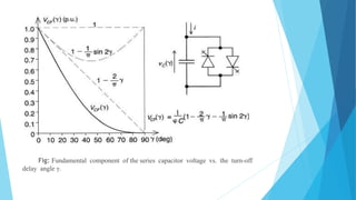
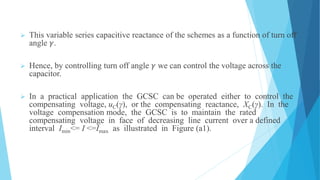
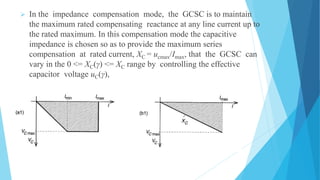


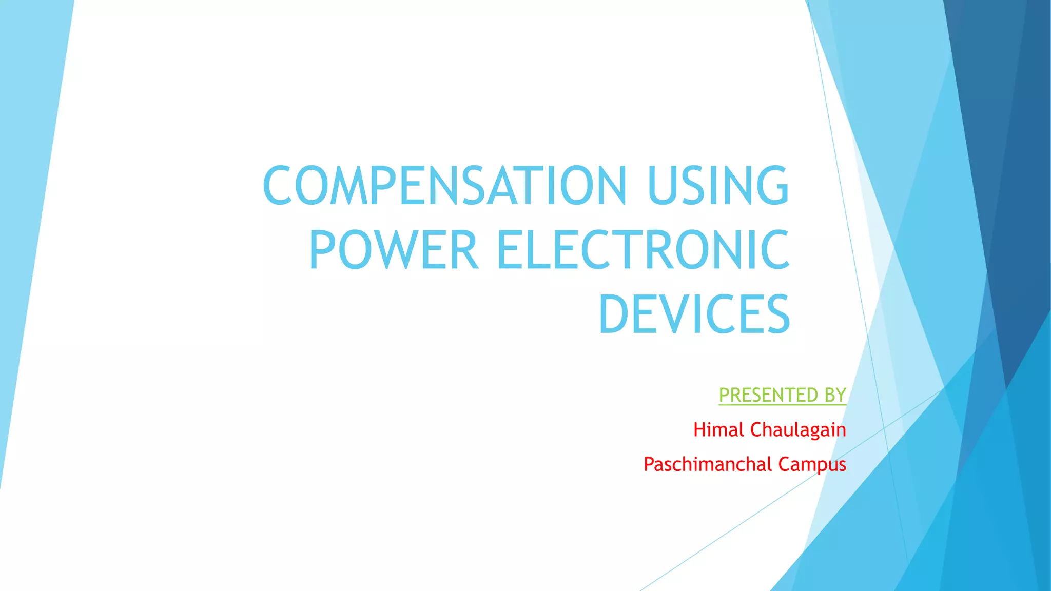
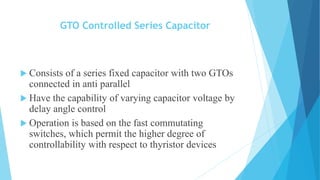
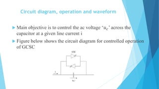
The document discusses GTO controlled series capacitor (GCSC) compensation for power transmission systems. GCSC consists of a series capacitor with two GTOs connected in anti-parallel to allow control of the capacitor voltage through delay angle control. By adjusting the delay angle of the GTO switches, the effective voltage across the capacitor can be varied each half cycle, providing a means to control the series capacitive reactance and compensate for varying line current. Mathematical expressions are presented relating the fundamental component of the capacitor voltage and reactance to the delay angle control. GCSC allows maintaining either a constant compensating voltage or maximum compensating reactance over a range of line currents.


