One gains knowledge from four sources: 1⁄4 from the teacher, 1⁄4 from self-study, 1⁄4 from classmates, and 1⁄4 from gaining experience over time. The document discusses the different sources from which one gains knowledge, with equal portions coming from the teacher, self-study, classmates, and experience over time.


![Important Formulae to Solve AM-DSB-FC problems
ma =
Vm
Vc
% modulation index, = max100
=(
Vm
Vc
)x100
Vmax = Vc+ Vm
Vmin = Vc - Vm
ma =
(Vmax − Vmin)
(Vmax+Vmin )
BW = 2fm
BW = f2 - f1
PC=
Vc
2
2𝑅
PLSB= PUSB =
ma
2
𝟒
PC
PT= PC +PLSB+ PUSB
PT = Pc[ 1 +
ma
2
𝟐
]
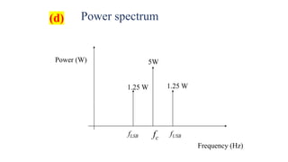
VAM (t) = Vc [1+ maCos 2πfmt] Cos 2πfCt
VAM (t) = Vc Cos ωC t +
maVc
𝟐
Cos(ωC + ωm)t +
maVc
𝟐
Cos(ωC - ωm)t
➢ AM Double sideband with FULL
carrier.](https://image.slidesharecdn.com/ce-classon14-200714080342/85/Communication-Engineering-class-5-10-320.jpg)
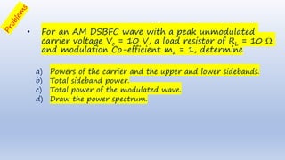
![Given,
➢ carrier voltage Vc = 10 V,
➢ Load resistor of RL = 10
➢ Modulation Co-efficient ma = 1.
PC=
Vc
2
2𝑅
=
102
2 (10)
=
100
2 (10)
= 5𝑊
PLSB= PUSB =
ma
2
𝟒
PC =
12
𝟒
(5)= 1.25W
PT = Pc[ 1 +
ma
2
𝟐
] = 5[ 1 +
12
𝟐
] =5[ 1 + 0.5 ] =5[ 1.5 ] = 7.5 W
Total Side band Power =PLSB+ PUSB = 1.25 W+ 1.25 W = 2.5 W
(a)
(b)
(c)](https://image.slidesharecdn.com/ce-classon14-200714080342/85/Communication-Engineering-class-5-15-320.jpg)
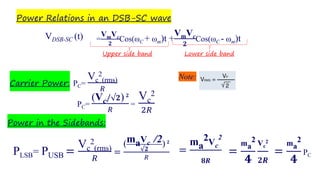
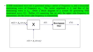
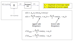
![VDBS-SC (t) =
= Vm Cos ωmt . VC Cos ωCt
=
VmVc
𝟐
[Cos(ωC + ωm)t + Cos(ωC - ωm)t]
Note:
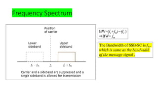
Frequency Spectrum of an DSB-SC wave:
BW=(fc+fm)−(fc −fm)
⇒BW=2fm](https://image.slidesharecdn.com/ce-classon14-200714080342/85/Communication-Engineering-class-5-19-320.jpg)
![If the carrier is suppressed,then the total power transmitted in
DSB-SC AM wave is,
P'T= PLSB+ PUSB
=
ma
2
𝟒
Vc
2
2𝑅
+
ma
2
𝟒
Vc
2
2𝑅
=
ma
2
𝟒
Pc+
ma
2
𝟒
Pc
= Pc [ ma
2
𝟒
+
ma
2
𝟒
]
P'T = Pc[ma
2
𝟐 ]
Note: During transmission, the
carrier term is suppressed.](https://image.slidesharecdn.com/ce-classon14-200714080342/85/Communication-Engineering-class-5-21-320.jpg)
![Power savings in DSB-SC wave is calculated as follows:
PDSB-SC =
PT −P′T
PT
=
Pc[ 𝟏+
ma
2
𝟐
] − Pc[ ma
2
𝟐
]
Pc[ 𝟏+
ma
2
𝟐
]
=
𝟏+
ma
2
𝟐
− ma
2
𝟐
𝟏+
ma
2
𝟐
=
𝟏
𝟏+
ma
2
𝟐
=
2
𝟐+ma
2
➢Therefore, the percentage of Power saving is given by,
=
2
𝟐+ma
2
x100
➢If modulation index , ma = 1,for 100% modulation, then the power
saving is given is calculated as, =
2
3
x 100 = 66.7 %](https://image.slidesharecdn.com/ce-classon14-200714080342/85/Communication-Engineering-class-5-22-320.jpg)
![Important Formulae to Solve AM-DSB-SC problems
ma =
Vm
Vc
% modulation index, = max100
=(
Vm
Vc
)x100
BW = 2fm
PC=
Vc
2
2𝑅
PLSB= PUSB =
ma
2
𝟒
PC
P'T = Pc[ma
2
𝟐
]
The total power transmitted in DSB-SC AM wave, P'T = Pc[ma
2
𝟐 ]
VDSB-SC (t) =
VmVc
𝟐
Cos(ωC + ωm)t +
VmVc
𝟐
Cos(ωC - ωm)t
➢The percentage of Power saving is given as =
2
𝟐+ma
2
x100](https://image.slidesharecdn.com/ce-classon14-200714080342/85/Communication-Engineering-class-5-23-320.jpg)

![Given,
➢ carrier voltage Vc = 10 V,
➢ Load resistor of RL = 10
➢ Modulating Signal fm = 10kHz
➢ Modulation Co-efficient ma = 1.
PC=
Vc
2
2𝑅
=
102
2 (10)
=
100
2 (10)
= 5𝑊
P'T = Pc[
ma
2
𝟐
] = 5[
12
𝟐
] =5[ 0.5 ] =5[ 0.5 ] = 2.5 W
(a)
(b)
(c) Bandwidth = 2fm = 2(10kHz) = 20 kHz
Power in Side bands, PLSB= PUSB =
ma
2
𝟒
PC =
12
𝟒
(5)= 1.25W](https://image.slidesharecdn.com/ce-classon14-200714080342/85/Communication-Engineering-class-5-25-320.jpg)
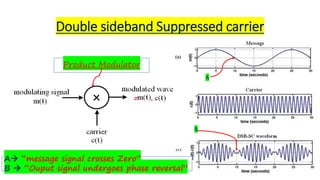
![Observations:
➢ Double sideband with Suppressed carrier.
➢The sum and difference frequencies are present.
➢Only 66.7% of saving of power is achieved.
➢Power consumed by LSB and USB are same.
➢The same information is transmitted twice . One in USB and another in LSB.
Target:
➢ How to improve Power Saving?
Answer: Eliminate one side band (USB or LSB) in addition to carrier .
Hence,one side band is enough for transmission as well as
recovering the useful information.
VDBS-SC (t) =
VmVc
𝟐
[Cos(ωC + ωm)t + Cos(ωC - ωm)t]
DSB-SC AM wave is given by,](https://image.slidesharecdn.com/ce-classon14-200714080342/85/Communication-Engineering-class-5-26-320.jpg)
![Total Power saved in SSB-SC is calculated as follows:
Power in SSB-SC is given by,
P'T= PUSB (or) PLSB
P'T =
ma
2
𝟒
Vc
2
2𝑅
=
ma
2
𝟒
Pc
PSSB-SC =
PT − P′T
PT
=
Pc[ 𝟏+
ma
2
𝟐
] − Pc[ ma
2
𝟒
]
Pc[ 𝟏+
ma
2
𝟐
]
=
𝟏+
ma
2
𝟐
− ma
2
𝟒
𝟏+
ma
2
𝟐
=
𝟏+
ma
2
𝟒
𝟏+
ma
2
𝟐
=
𝟒+ma
2
𝟐( 𝟐+ma
2)
=
𝟒+ma
2
𝟒+𝟐ma
2
➢If modulation index , ma = 1,for 100% modulation, then the power saving
is given is calculated as, =
5
6
x 100 = 83.33 %](https://image.slidesharecdn.com/ce-classon14-200714080342/85/Communication-Engineering-class-5-31-320.jpg)
![Important Formulae to Solve AM-SSB-SC problems
ma =
Vm
Vc
% modulation index, = max100
=(
Vm
Vc
)x100
BW = fm
PC=
Vc
2
2𝑅
PLSB= PUSB =
ma
2
𝟒
PC
P'T = Pc[ma
2
𝟒
]
The total power transmitted in SSB-SC AM wave, P'T = Pc[
ma
2
𝟒
]
VSSB-SC (t) =
VmVc
𝟐
Cos(ωC + ωm)t OR
VmVc
𝟐
Cos(ωC - ωm)t
➢The percentage of Power saving is given as ==
𝟒+ma
2
𝟒+𝟐ma
2
x100](https://image.slidesharecdn.com/ce-classon14-200714080342/85/Communication-Engineering-class-5-32-320.jpg)
![Given,
➢ carrier voltage Vc = 10 V,
➢ Load resistor of RL = 10
➢ Modulating Signal fm = 10kHz
➢ Modulation Co-efficient ma = 1.
PC=
Vc
2
2𝑅
=
102
2 (10)
=
100
2 (10)
= 5𝑊
P'T = Pc[
ma
2
𝟒
] = 5[
12
𝟒
] =5[ 0.25 ] = 1.25 W
(a)
(b)
(c) Bandwidth = fm = 10kHz
Power in Side band, PLSB or PUSB =
ma
2
𝟒
PC =
12
𝟒
(5)= 1.25W](https://image.slidesharecdn.com/ce-classon14-200714080342/85/Communication-Engineering-class-5-34-320.jpg)