This document provides an overview of logic circuits and their components. It introduces basic logic gates like AND, OR, NAND, and NOR gates. It explains how these gates can be combined to build more complex logic circuits and discusses different types of logic circuits like bistables and flip-flops. It also covers integrated circuit logic devices and different scales of integration.
The document discusses basic and derived logic gates. It begins by introducing Boolean algebra and defining logic 0 and 1. It then explains the three basic logic gates - OR, AND, and NOT - through truth tables and circuit diagrams. The OR gate's output is 1 if any input is 1. The AND gate's output is 1 only if all inputs are 1. The NOT gate inverts the input. Complex logic circuits can be described algebraically using these basic gates and Boolean operations.
Digital logic gates are the basic building blocks of digital circuits. The three main types of logic gates are AND gates, OR gates, and NOT gates. Logic gates have one or more inputs and one output, and the output depends on the combinations of inputs according to truth tables. Common logic gates include AND, OR, NAND, NOR, XOR, and XNOR gates. Logic gates can be combined to perform more complex logical operations and form the basis of digital electronics in computers and other devices.
This document discusses digital logic gates. It begins by defining a gate as a digital circuit with one or more inputs and one output. The three basic gates are described as the NOT, OR, and AND gates. Additional universal gates, the NAND and NOR gates, are introduced. Truth tables are provided to explain the output of each gate for all possible input combinations. The document also discusses how to derive different gate functions using NAND and NOR gates alone through De Morgan's theorems.
FYBSC IT Digital Electronics Unit II Chapter I Boolean Algebra and Logic GatesArti Parab Academics
Boolean Algebra and Logic Gates:
Introduction, Logic (AND OR NOT), Boolean theorems, Boolean
Laws, De Morgan’s Theorem, Perfect Induction, Reduction of Logic
expression using Boolean Algebra, Deriving Boolean expression from
given circuit, exclusive OR and Exclusive NOR gates, Universal Logic
gates, Implementation of other gates using universal gates, Input
bubbled logic, Assertion level.
This document provides an overview of digital electronics and electronic principles. It covers topics such as number systems, binary codes, Boolean algebra, logic gates, and applications of digital circuits. Number systems and conversions between binary, decimal, octal, and hexadecimal are examined. Boolean algebra and logic gates like AND, OR, NOT, NAND, and NOR are described along with their truth tables. Combinational logic circuits including adders, multiplexers, and decoders are discussed. Sequential logic and memory elements like latches and flip-flops are also introduced. The document provides fundamental information on digital electronics and serves as an introduction to the key concepts and components in the field.
boolean algrebra and logic gates in shortRojin Khadka
The document discusses logic gates and Boolean algebra. It describes the basic logic gates - OR, AND, NOT, NAND, NOR and XOR gates. It explains their symbols, truth tables and functions. Logic gates are electronic circuits that make logic decisions. Boolean algebra uses values of 0 and 1 instead of numbers. It has laws like commutative, associative and distributive laws that define operations on logic values. Logic gates and Boolean algebra are important for designing digital circuits and simplifying logical functions.
Logic gates process true and false signals to perform logic functions. The key logic gates are NOT, AND, NAND, OR, NOR, EX-OR, and EX-NOR. Gates have standardized symbols and can be combined to create more complex logic functions. NAND and NOR gates are particularly useful because any other gate can be created by combining NAND or NOR gates.
The document discusses various logic gates and flip flops. It begins by explaining the AND, OR, and NOT gates as the fundamental logic gates. It then discusses the JK flip flop, explaining its operation and how it can be used to create counters. It also briefly discusses the SR flip flop and D flip flop. The document provides truth tables and diagrams to illustrate the working of these logic components.
The document describes a student's practice assignment on Boolean algebra using logic gates. It includes an introduction explaining the importance of understanding logic gates and their characteristics based on Boolean algebra. The main body defines common logic gates like AND, OR, NOT, NAND, NOR and XOR. It then shows how to simulate the logic gates using Multisim software and check their truth tables. The document concludes by using the basic gates to implement a half adder circuit and check its truth table.
Logic gates form the basic building blocks of digital circuits and logic. The three fundamental logic gates are AND, OR, and NOT. NAND and NOR gates are also commonly used as they are universal gates that can be combined to perform all possible logic functions. Techniques for minimizing logic expressions include Karnaugh maps, which allow visualization of minterms, and the Quine-McCluskey method, which systematically finds prime implicants. Implementation of logic functions typically uses NAND or NOR gates due to their simplicity and universality.
M. FLORENCE DAYANA/unit - II logic gates and circuits.pdfDr.Florence Dayana
Logic Gates, Truth Table, AND Gate
Types of Digital Logic AND Gate, The 2-input and 3-input AND Gate, OR Gate, Types of Digital Logic AND Gate, The 2-input OR gate, The 3-input OR gate, NOT Gate, NAND Gate, The 2-input NAND Gate, The 3-input NAND Gate, NOR Gate, 2-input NOR gate
Just like other gates, XOR gate or Exclusive-OR gate
Digital logic is based on the binary number system of 0s and 1s. This two-valued logic system allows statements to be either true or false. One reason for using binary is that electronic circuits can be designed to reliably represent and switch between two states. There are two classes of digital logic - combinational logic, where outputs depend only on current inputs, and sequential logic, where outputs also depend on prior states. Basic logic gates like AND, OR, and NOT are used to combine input signals in circuits. The Karnaugh map provides a visual method to simplify Boolean logic expressions by grouping adjacent ones to minimize variables.
This document provides an introduction to programming programmable logic controllers (PLCs) using ladder diagrams, functional block diagrams, and statement list languages. It describes the basic techniques for developing ladder and function block programs representing logic functions like AND, OR, XOR, NAND and NOR. Specific topics covered include ladder diagram conventions, logic gates and truth tables, and latching circuits to hold an output energized even after the input ceases. Examples are provided of drawing ladder diagrams for logic functions and latching circuits to control devices like motors.
There are three main ways to represent gates and circuits: logic diagrams using symbolic drawings, truth tables listing all input-output combinations, and Boolean expressions using algebraic notation. The document then describes the seven basic logic gates - NOT, AND, OR, XOR, NAND, NOR, and XNOR - showing their truth tables, symbols, and examples of practical applications. It explains that NOT, AND and OR are the fundamental gates, while NAND and NOR are considered "universal gates" since all others can be constructed from them.
This document discusses basic logic concepts used in ladder logic programming including gates, latch/unlatch coils, and processor status files. It introduces binary concepts and how gates like AND, OR, NOT, NAND, NOR, and XOR make decisions. Examples of gate circuits are shown in electromechanical and PLC/PAC ladder diagrams. Latch and unlatch coils are used to control outputs and the first scan bit is identified as a useful processor status address.
This document provides an overview of gates and circuits in computing. It discusses the basic logic gates (NOT, AND, OR, XOR, NAND, NOR) and how they are implemented using transistors. It describes how gates can be combined into more complex circuits and various ways to represent circuits using Boolean expressions, truth tables, and logic diagrams. The document also covers adders, multiplexers, circuits used for memory like S-R latches, and the four generations of integrated circuits.
This document provides an overview of gates and circuits in computing. It describes the basic logic gates (NOT, AND, OR, XOR, NAND, NOR) and how they are implemented using transistors. It explains how gates can be combined into more complex circuits and various ways to represent circuits using Boolean expressions, truth tables, and logic diagrams. The document also discusses adders, multiplexers, latches for memory, and integrated circuits.
This document provides an introduction to basic logic gates. It includes:
1. An introduction that defines logic gates and their use of diodes to allow or block signals based on logic conditions.
2. Descriptions of three basic logic gates - OR, AND, and NOT - including their symbols, Boolean expressions, and truth tables.
3. Sections on each of the three basic gates that explain how to simulate them using components like diodes, transistors, and resistors, and provide examples of their truth tables.
The document serves as an overview of logic gates, their components, representations, and functions as basic building blocks of digital circuits.
This document discusses Boolean logic and logic gates. It describes the basic logic gates - NOT, AND, and OR - and how more complex gates like NAND and NOR are derived from them. It also covers Boolean logic concepts like duality, De Morgan's theorems, and how logic gates can be combined into circuits to perform decision making and memory functions. Applications of logic gates include systems for genetic engineering, nanotechnology, industrial processes and medicine.
Digital logic gates and Boolean algebraSARITHA REDDY
The document discusses digital logic gates and Boolean algebra. It defines logic gates as electronic circuits that make logic decisions. Common logic gates include OR, AND, and NOT gates. Boolean algebra uses truth values of 0 and 1 instead of numbers, and has fundamental laws and operations for AND, OR, and NOT. Boolean algebra can be used to simplify logical expressions and save gates in digital circuit design.
The document discusses different digital logic components including logic gates, flip flops, registers, and counters. It describes the basic types of logic gates such as AND, OR, NOT, NAND, and NOR gates. It also discusses different types of flip flops including T, S-R, J-K, and D flip flops which are used to store binary data. Registers are formed using groups of flip flops to store multi-bit data. Counters are also discussed as another component of digital logic systems.
Logic gates are basic electronic circuits that perform logical operations and produce binary outputs. The common logic gates are OR, AND, NOT, NAND, NOR, XOR, and XNOR. An OR gate output is 1 if one or more inputs are 1. An AND gate output is 1 only if all inputs are 1. A NOT gate inverts the input so its output is the opposite state. Combinations of gates can create more complex gates like NAND and NOR. Logic gates have applications in electronic devices like alarms and locks.
This document discusses digital logic design and covers the following topics:
- It outlines the course grading breakdown of a digital logic design course.
- It introduces basic logic gates like AND, OR, NOT and describes how they are combined to build half adders and full adders.
- It explains logic gates in detail including Boolean expressions, truth tables and logic diagrams. Transistors are described as the basic building blocks of computers that are combined to implement logic functions.
The document discusses logic gates and Boolean algebra. It defines key logic gate terms like AND, OR, NAND, NOR, and XOR gates. It provides truth tables that define the output of each gate based on all possible input combinations. Boolean algebra laws and operations are also covered, including addition, multiplication, commutative laws, associative laws, and the distributive law. Methods for converting between Boolean expressions, truth tables, and logic circuits are described. Examples are provided to illustrate how to derive the expression, truth table, or circuit from one of the other representations.
Introduction- e - waste – definition - sources of e-waste– hazardous substances in e-waste - effects of e-waste on environment and human health- need for e-waste management– e-waste handling rules - waste minimization techniques for managing e-waste – recycling of e-waste - disposal treatment methods of e- waste – mechanism of extraction of precious metal from leaching solution-global Scenario of E-waste – E-waste in India- case studies.
Low power architecture of logic gates using adiabatic techniquesnooriasukmaningtyas
The growing significance of portable systems to limit power consumption in ultra-large-scale-integration chips of very high density, has recently led to rapid and inventive progresses in low-power design. The most effective technique is adiabatic logic circuit design in energy-efficient hardware. This paper presents two adiabatic approaches for the design of low power circuits, modified positive feedback adiabatic logic (modified PFAL) and the other is direct current diode based positive feedback adiabatic logic (DC-DB PFAL). Logic gates are the preliminary components in any digital circuit design. By improving the performance of basic gates, one can improvise the whole system performance. In this paper proposed circuit design of the low power architecture of OR/NOR, AND/NAND, and XOR/XNOR gates are presented using the said approaches and their results are analyzed for powerdissipation, delay, power-delay-product and rise time and compared with the other adiabatic techniques along with the conventional complementary metal oxide semiconductor (CMOS) designs reported in the literature. It has been found that the designs with DC-DB PFAL technique outperform with the percentage improvement of 65% for NOR gate and 7% for NAND gate and 34% for XNOR gate over the modified PFAL techniques at 10 MHz respectively.
ACEP Magazine edition 4th launched on 05.06.2024Rahul
This document provides information about the third edition of the magazine "Sthapatya" published by the Association of Civil Engineers (Practicing) Aurangabad. It includes messages from current and past presidents of ACEP, memories and photos from past ACEP events, information on life time achievement awards given by ACEP, and a technical article on concrete maintenance, repairs and strengthening. The document highlights activities of ACEP and provides a technical educational article for members.
12. Introduction
The logic circuits are used extensively in digital systems and form
the basis of clocks, counters, shift registers and timers.
Some basic logic gate like NOT, AND, OR, the special logic gates
like Exclusive-OR, Exclusive NOR and universal logic gate like
NAND and NOR are introduced.
Their symbols, truth table are that describes their operations are
explained.
Further, it has been explained to construct a combinational logic
circuits using above gates and also about how to identify the digital
devices according to semiconductor technology-TTL or CMOS.
13. Logic functions
Electronic logic circuits can be used to make simple decisions like:
1) If dark then put on the light.
2) If temperature is less then 20°C then connect the supply to the heater.
They can also be used to make more complex decisions like:
If ‘hour’ is greater than 11 and ‘24 hour clock’ is not selected then display
message ‘pm’.
14. Logic functions
All of these logical statements are similar in form.
The first two are essentially:
If {condition} then {action}.
while the third is a compound statement of the form:
If {condition 1} and not {condition 2} then {action}.
Both of these statements can be readily implemented using
straightforward electronic circuits.
Because this circuitry is based on discrete states and since the
behavior of the circuits can be described by a set of logical
statements, it is referred to as digital logic.
15. Switch and lamp logic
In the simple circuit shown in Figure 4.1 a battery is connected to a
lamp via a switch.
There are two possible states for the switch, open and close.
Lamp will only operate when the switch is closed.
The logical state of the switch can be represented by the binary
digits, 0 and 1.
That is, if logical 0 is synonymous with open (or ‘off’) and logical 1 is
equivalent to closed (or ‘on’), then:
Switch open (off) = 0
Switch closed (on) = 1
16. Switch and lamp logic
Figure 4.1 Simple switch and lamp
circuit
Condition Switch Comment
1 Open No light produced
2 Closed Light produced
Table 4.1 Simple switching logic
Figure 4.2 Truth table for the switch and lamp
17. AND logic
Figure 4.3 AND switch and lamp logic
Table 4.2 Simple AND switching logic
Table 4.3 Truth table for the AND logic
Condition Switch A Switch B Comment
1 Open Open No light
produced
2 Open Closed No light
produced
3 Closed Open No light
produced
4 Closed Closed Light produced
18. AND logic
The AND function is explained once again by using the simple switch and
light system as shown in Figure 4.3.
The related circuit can be easily understood through truth table shown in
Table 4.2.
Here the lamp will only operate when switch A is closed and switch B is
closed.
Since there are two switches (A and B) and there are two possible states for
each switch (open or closed), there is a total of four possible conditions for
the circuit.
Each switch can only be in one of the two states (i.e. open or closed) at any
given time, the open and closed conditions are mutually exclusive.
19. AND logic
Furthermore, since the switches cannot exist in any other state than
completely open or completely closed (i.e. there are no intermediate states)
the circuit uses binary logic.
We can thus represent the logical states of the two switches by the binary
digits, 0 and 1.
Once again, if we adopt the convention that an open switch can be
represented by 0 and a closed switch by 1, we can rewrite the truth table in
terms of the binary states shown in table 4.3 where:
No light (off) = 0
Light (on) = 1
20. OR logic
Figure 4.4 OR switch and lamp logic
Table 4.2 Simple OR switching logic
Table 4.5 Truth table for OR logic
Condition Switch A Switch B Comment
1 Open Open No light produced
2 Open Closed Light produced
3 Closed Open Light produced
4 Closed Closed Light produced
A B Y
0 0 0
0 1 1
1 0 1
1 1 1
21. OR logic
Figure 4.4 shows another circuit with two switches.
This circuit differs from that shown in Figure 4.3 by virtue of the fact
that the two switches are connected in parallel rather than in series.
In this case the lamp will operate when either of the two switches is
closed. There are four possible conditions for the circuit.
We can summarize these conditions in Table 4.4.
Once again, adopting the convention that an open switch can be
represented by 0 and a closed switch by 1, we can rewrite the truth
table in terms of the binary states as shown in Table 4.5.
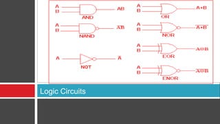
22. Logic gates
Logic gates are circuits designed to produce the basic logic functions,
AND, OR, etc.
These circuits are designed to be interconnected into larger, more
complex, logic circuit arrangements.
Since these circuits form the basic building blocks of all digital systems, we
have summarized the action of each of the gates in the next section.
For each gate we have included its British Standard (BS) symbol together
with its American Standard (MIL/ANSI) symbol.
We have also included the truth tables and Boolean expressions (using ‘+’
to denote OR, ‘·’ to denote AND, and ‘E’ to denote NOT).
Note that, while inverters and buffers each have only one input, exclusive-
OR gates have two inputs and the other basic gates (AND, OR, NAND and
23. Buffers
Buffers do not affect the logical state of a digital signal (i.e. a logic 1
input results in a logic 1 output whereas a logic 0 input results in a logic
0 output).
Buffers are normally used to provide extra current drive at the output
but can also be used to regularize the logic levels present at an
interface.
The Boolean expression for the output, Y, of a buffer with an input, X,
is: Y = X.
Figure 4.5 Symbols and truth table for a buffer
24. Inverters
Inverters are used to complement the logical state (i.e. a logic 1 input
results in a logic 0 output and vice versa). Inverters also provide extra
current drive and, like buffers, are used in interfacing applications
where they provide a means of regularizing logic levels present at the
input or output of a digital system.
The Boolean expression for the output, Y, of a inverter with an input, X,
is: Y =X
Figure 4.6 Symbols and truth table for an Inverter
25. AND gate
AND gates will only produce a logic 1 output when all inputs are
simultaneously at logic 1.
Any other input combination results in a logic 0 output.
The Boolean expression for the output, Y, of an AND gate with inputs,
A and B, is: Y =A.B
Figure 4.7 Symbols and truth table for an AND Gate
26. OR gate
OR gates will produce a logic 1 output whenever anyone, or more,
inputs are at logic 1.
Putting this in another way, an OR gate will only produce a logic 0
output whenever all of its inputs are simultaneously at logic 0.
The Boolean expression for the output, Y, of an OR gate with inputs, A
and B, is:
Y =A+B
Figure 4.8 Symbols and truth table for an OR Gate
27. NAND gate
NAND (i.e. NOT-AND) gates will only produce a logic 0 output when all inputs
are simultaneously at logic 1.
Any other input combination will produce a logic 1 output. A NAND gate,
therefore, is nothing more than an AND gate with its output inverted! The circle
shown at the output denotes this inversion.
The Boolean expression for the output, Y, of a NAND gate with inputs, A and B,
is:
Y =A.B
Figure 4.9 Symbols and truth table for a NAND Gate
28. NOR gate
NOR (i.e. NOT-OR) gates will only produce a logic 1 output when all inputs are
simultaneously at logic 0.
Any other input combination will produce a logic 0 output. A NOR gate,
therefore, is simply an OR gate with its output inverted.
A circle is again used to indicate inversion. The Boolean expression for the
output, Y, of a NOR gate with inputs, A and B, is: Y =A+B
Figure 4.10 Symbols and truth table for a NOR Gate
29. Exclusive-OR gates
Exclusive-OR gates will produce a logic 1 output whenever either one of the
inputs is at logic 1 and the other is at logic 0.
Exclusive-OR gates produce a logic 0 output whenever both inputs have the
same logical state (i.e. when both are at logic 0 or both are at logic 1).
The Boolean expression for the output, Y, of an exclusive-OR gate with inputs,
A and B, is: Y =A.B+B.A
Figure 4.11 Symbols and truth table for an exclusive-OR gate
30. Combinational logic
By using a standard range of logic levels (i.e. voltage levels used to
represent the logic 1 and logic 0 states) logic circuits can be
combined together in order to solve complex logic functions.
The output of a bistable has two stables states (logic 0 or logic 1)
and, once set in one or other of these states, the device will remain
at a particular logic level for an indefinite period until reset.
A bistable thus constitutes a simple form of ‘memory cell’ because it
will remain in its latched state (whether set or reset) until a signal is
applied to it in order to change its state (or until the supply is
disconnected).
78. R-S bistables
The simplest form of bistable is the R-S bistable. This device has two inputs,
SET and RESET, and complementary outputs, Q and Q.
A logic 1 applied to the SET input will cause the Q output to become (or remain
at) logic 1 while a logic 1 applied to the RESET input will cause the Q output to
become (or remain at) logic 0.
In either case, the bistable will remain in its SET or RESET state until an input is
applied in such a sense as to change the state. Two simple forms of R-S
bistable based on cross-coupled logic gates are shown in Figure 4.12.
Figure 4.12(a) is based on NAND gates while Figure 4.12(b) is based on NOR
gates.
The simple cross-coupled logic gate bistable has a number of serious
shortcomings (consider what would happen if a logic 1 was simultaneously
present on both the SET and RESET inputs!) and practical forms of bistable
make use of much improved purpose-designed logic circuits such as D-type and
79. D-type bistables
The D-type bistable has two inputs: D (standing variously for ‘data’
or ‘delay’) and CLOCK (CLK).
The data input (logic 0 or logic 1) is clocked into the bistable such
that the output state only changes when the clock changes state.
Operation is thus said to be synchronous. Additional subsidiary
inputs (which are invariably active low) are provided which can be
used to directly set or reset the bistable. These are usually called
PRESET (PR) and CLEAR (CLR).
D-type bistables are used both as latches (a simple form of memory)
and as binary dividers.
82. D-type bistables – Timing diagram
Figure 4.14 Timing diagram for the D-type Bistable
83. J-K bistables
J-K bistables have two clocked inputs (J and K), two direct inputs
(PRESET and CLEAR), a CLOCK (CK) input, and outputs (Q and
Q).
As with R-S bistables, the two outputs are complementary (i.e. when
one is 0 the other is 1, and vice versa).
Similarly, the PRESET and CLEAR inputs are invariably both active
low (i.e. a 0 on the PRESET input will set the Q output to 1 whereas
a 0 on the CLEAR input will set the Q output to 0).
Tables 4.6 and 4.7 summarize the operation of a J-K bistable
respectively for the PRESET and CLEAR inputs and for clocked
operation.
88. J-K bistables
Table 4.6 Input and output states for a J-K bistable (PRESET and CLEAR inputs)
Inputs
Output (QN+1)
Comments
PRESET CLEAR
0 0 ? Indeterminate
0 1 0
Q output changes to 0
(i.e. Q is reset) regardless
of the clock state
1 0 1
Q output changes to 1
(i.e. Q is set) regardless
of the clock state
1 1 See below operation (refer to Table 4.7)
Note: The preset and clear inputs operate regardless of the clock.
89. J-K bistables
Table 4.7 Input and output states for a J-K bistable (clocked operation)
Inputs
Output (QN+1)
Comments
J K
0 0 QN
No change in state of the
Q output on the next clock transition
0 1 0
Q output changes to 0
(i.e. Q is reset) on the next clock transition
1 0 1
Q output changes to 1 (i.e. Q is set)
on the next clock transition
1 1 QN
Q output changes to the opposite state
on the next clock transition
Note: QN+1 means ‘Q after the next clock transition’ while QN means ‘Q in whatever state it was before’.
91. J-K bistables
J-K bistables are the most sophisticated and flexible of the bistable types and
they can be configured in various ways including binary dividers, shift registers,
and latches.
Figure 4.15 shows the arrangement of a four stage binary counter based on J-K
bistables.
The timing diagram for this circuit is shown in Figure 4.16. Each stage
successively divides the clock input signal by a factor of two.
Note that a logic 1 input is transferred to the respective Q-output on the falling
edge of the clock pulse and all J and K inputs must be taken to logic 1 to enable
binary counting.
Figure 4.17 shows the arrangement of a four stage shift register based on J-K
bistables. The timing diagram for this circuit is shown in Figure 4.18. Note that
each stage successively feeds data to the next stage. Note that all data transfer
94. Integrated circuit logic devices
The task of realizing a complex logic circuit is made simple with the
aid of digital integrated circuits.
Such devices are classified according to the semiconductor
technology used in their fabrication (the logic family to which a
device belongs is largely instrumental in determining its operational
characteristics, such as power consumption, speed and immunity to
noise).
The relative size of a digital integrated circuit (in terms of the
number of active devices that it contains) is often referred to as its
scale of integration and the terminology in Table 4.8 is commonly
used.
95. Integrated circuit logic devices
Table 4.8 Scale of integration
Scale of
integration
Abbreviation Number of logic
gates*
Small SSI 1 to 10
Medium MSI 10 to 100
Large LSI 100 to 1,000
Very large VLSI 1,000 to 10,000
Super large SLSI SLSI 10,000 to 100,000
* or active circuitry of equivalent complexity
96. Integrated circuit logic devices
The two basic logic families are CMOS (complementary metal oxide
semiconductor) and TTL (transistor transistor logic).
Each of these families is then further sub-divided. The most
common family of TTL logic devices is known as the 74-series.
Devices from this family are coded with the prefix number 74.
Variants within the family are identified by letters which follow the
initial 74 prefix, as shown in Table 4.9.
The most common family of CMOS devices is known as the 4000-
series. Variants within the family are identified by the suffix letters
given in Table 4.10.
97. Integrated circuit logic devices
Table 4.9 TTL device coding - infix letters
Infix Meaning
None Standard TTL device
ALS Advanced low-power Schottky
C CMOS version of a TTL device
F ‘Fast’ (a high-speed version)
H High-speed version
S Schottky input configuration (improved
speed and noise immunity)
HC High-speed CMOS version (CMOS
compatible
inputs)
HCT HCT High-speed CMOS version (TTL
compatible
inputs)
LS Low-power Schottky
98. Integrated circuit logic devices
Table 4.10 CMOS device coding the most common variants of the
4000 family are identified using these suffix letters
Infix Meaning
A Standard CMOS device
None Standard (unbuffered) CMOS device
B, BE Improved (buffered) CMOS device
UB, UBE Improved (unbuffered) CMOS device