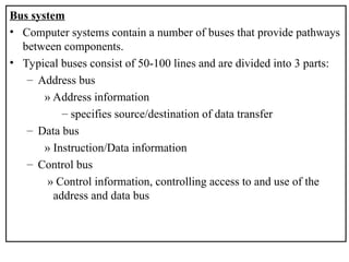
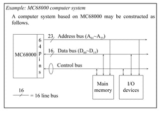
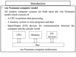
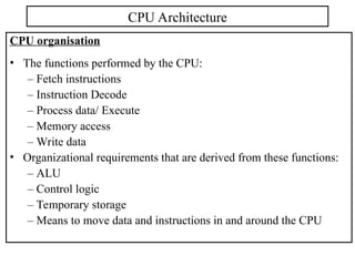
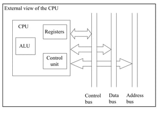
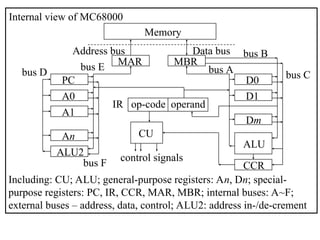
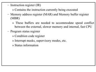
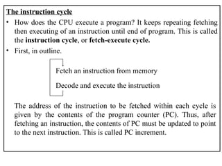
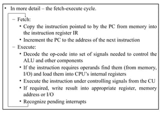
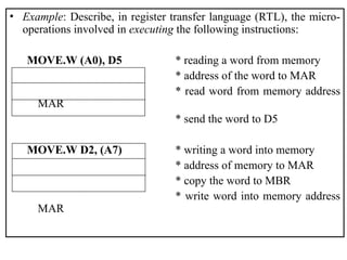
Computer Architecture
Course EE3213
Basic Computer Architecture
• Overview
– CPU
Register organisation, instruction cycle, control unit
– Memory
Hierarchy, main memory, cache memory
– Input/Output
Programmed I/O, interrupt-driven I/O, DMA
– Interconnection structures
Bus systems
Introduction
• von Neumann computer model
All modern computer systems are built upon the von Neumann
model which consists of
– A CPU to perform data processing
– A memory system to store programs and data
– Input/Output (I/O) devices for communication between the
computer and the outside world
Memory I/O
devices
CPU
Bus
von Neumann computer architecture
CPU organisation
• The functions performed by the CPU:
– Fetch instructions
– Instruction Decode
– Process data/ Execute
– Memory access
– Write data
• Organizational requirements that are derived from these functions:
– ALU
– Control logic
– Temporary storage
– Means to move data and instructions in and around the CPU
CPU Architecture
External view of the CPU
ALU
Registers
Control
unit
CPU
Control
bus
Data
bus
Address
bus
Internal view of MC68000
Including: CU; ALU; general-purpose registers: An, Dn; special-
purpose registers: PC, IR, CCR, MAR, MBR; internal buses: A~F;
external buses – address, data, control; ALU2: address in-/de-crement
bus D
bus B
PC
A0
A1
An
D0
D1
Dm
IR op-code operand
ALU
MAR MBR
CCR
CU
ALU2
control signals
bus A bus C
bus E
bus F
Address bus Data bus
Memory
Register organisation
• Registers form the highest level of the memory hierarchy
– Small set of high speed (but electronically complex) storage
locations inside CPU
– Temporary storage for data and control information
• Two types of registers
– User-visible
» May be referenced by assembly-level instructions and are
thus “visible” to the user
– Control and status registers
» Used to control the operation of the CPU
» Most are not visible to the user
User-visible registers
• General-purpose registers
– Data registers (e.g. D0~D7 in MC68000)
» These registers only hold data
– Address registers (e.g. A0~A7 in MC68000)
» These registers hold address information
» Examples: address register indirect addressing (A0), (A1)+,
–(A2), –6(A3), stack pointers
» They may also be used for holding data
• Condition code registers
– Visible to the user but values set by the CPU as the result of
performing operations
– Example code bits: zero (Z), negative (N), overflow (V)
– Bit values are used as the basis for conditional jump instructions
Control and status registers
• These registers are used during the fetching, decoding and
execution of instructions
– Many are not visible to the user/programmer
– Some are visible but can not be (easily) modified
• Typical registers
– Program counter (PC)
» stores the memory address of the instruction to be executed
next
» automatically updated to the next instruction position after an
instruction is fetched from memory
» branches, subroutine calls and interrupts force PC to change
to a different value from its routine increment, so change the
flow of the program
– Instruction register (IR)
» Contains the instruction currently being executed
– Memory address register (MAR) and Memory buffer register
(MBR)
» These buffers are needed to accommodate speed conflict
between the external, slower memory and internal, fast CPU
– Program status register
» Condition code register
» Interrupt masks, supervisory modes, etc.
» Status information
The instruction cycle
• How does the CPU execute a program? It keeps repeating fetching
then executing of an instruction until end of program. This is called
the instruction cycle, or fetch-execute cycle.
• First, in outline.
Fetch an instruction from memory
Decode and execute the instruction
The address of the instruction to be fetched within each cycle is
given by the contents of the program counter (PC). Thus, after
fetching an instruction, the contents of PC must be updated to point
to the next instruction. This is called PC increment.
• In more detail – the fetch-execute cycle.
– Fetch:
• Copy the instruction pointed to by the PC from memory into
the instruction register IR
• Increment the PC to the address of the next instruction
– Execute:
• Decode the op-code into set of signals needed to control the
ALU and other components
• If the instruction requires operands find them (from memory,
I/O) and load them into CPU’s internal registers
• Execute the instruction under controlling signals from the CU
• If required, write result into appropriate register, memory
address or I/O
• Recognize pending interrupts
Register transfer language (RTL)
• To describe the details of operation of the CPU, we use a simple
language called RTL. The notations are as follows:
– Reg denotes contents of register Reg; Reg may be, for example,
MAR, MBR, PC, IR, D0, A5, ….
– Mem[x] denotes contents of a memory cell with address x;
sometimes [x].
– Mem[Reg] denotes contents of a memory cell whose address is
given by the contents of register Reg; sometimes [Reg].
– We use  to denote transfer of contents: MAR  PC means that
the contents of PC are transferred into MAR; PC  Mem[x]
means that the contents of address x are transferred into PC; and,
Mem[x]  PC means that the contents of PC are stored in
memory address x.
• Example: In RTL, the fetch-execute cycle for the instruction
ADD.W ($2000), D0 (in MC68000 assembly
language)
i.e. add the contents of memory address $2000 to the contents of a
data register D0 and store the result in D0 – can be expressed as
(assume that each instruction is 16 bits wide, or 2 bytes wide):
MAR  PC move contents of PC to MAR
PC  PC + 2 increment PC by 2 (why 2 ?)
MBR  Mem[MAR] read instruction from memory
IR  MBR move instruction to IR
CU  IR(op-code) move op-code to CU
MAR  IR(address) operand address ($2000) to MAR
MBR  Mem[MAR] read operand from memory
ALU  MBR, D0 perform addition
D0  ALU move output of ALU to D0
• Example: Describe, in register transfer language (RTL), the micro-
operations involved in executing the following instructions:
MOVE.W (A0), D5 * reading a word from memory
* address of the word to MAR
* read word from memory address
MAR
* send the word to D5
MOVE.W D2, (A7) * writing a word into memory
* address of memory to MAR
* copy the word to MBR
* write word into memory address
MAR
The control unit (CU)
• The CU is the most complex section in a CPU. It decodes the
instruction in the instruction register (IR), and generates signals that
control all parts of the CPU to execute the instruction.
• Two different approaches have been used to implement the CU:
hardwiring – seen in early computers, and microprogramming –
adopted by most modern computers.
Hardwiring
• Each instruction is executed directly by logic circuit – hardware. To
do this, all one has to do is ask what sequence of logical and
arithmetic operations are needed to carry out an instruction, and
then to design the appropriate logic circuit to bring this about.
• This is the technique used until the early 1960s.
Microprogramming
• This method was introduced in 1951 by Wilkes.
• Microprogramming means that each instruction could be translated
into a sequence of even more primitive instructions called
microinstructions, which specify the control signals for the
electronic components in every detail.
• For example, the operation ‘fetch an instruction’ in a fetch-execute
cycle can be decomposed into microinstructions as follows
MAR  PC move contents of PC to MAR
PC  PC + 2 increment PC by 2 (for 16 bit
machine)
MBR  Mem[MAR] read instruction from memory
IR  MBR move instruction to IR
CU  IR(op-code) move op-code to CU
• Microprogram is classified at the second lowest machine level, just
above the hardware - logic circuit. It is mainly the province of the
computer designer; and it comes as part of the CPU. For this reason,
it is often referred to as firmware – between hardware and
software.
Microprogram control vs. hardware control
• Microprogrammed solution
– allows arbitrarily complex instructions to be built-up;
– may also be more flexible, for example, there were some
machines that users could microprogram themselves;
– and, there were computers which differed only by their
microprograms, perhaps one optimised for execution of C
programs, another for PASCAL programs.
• Hardware solution
– hardware circuit is capable of decoding an instruction in ONE
clock period, i.e. a lot faster than the microprogrammed solution.
Memory Hierarchy
• The time spent for memory access has been a major factor limiting
the speed of a computer
– Memory speed is slow compared to the speed of the processor
– A process could be bottlenecked due to the inability of the
memory system to “keep up” with the processor
• Major design objective - to provide adequate storage capacity
– at an acceptable level of performance
– at a reasonable cost
Memory
Typical memory hierarchy: (Technology, size, access time)
Registers
in CPU
Cache
(RAM, 100sKB, ~10ns)
Main memory
(RAM, 100sMB~GB, ~50ns)
Magnetic disk
(Hard disk, 10sGB-100sGB, ~10ms)
Optical disk
(CD-ROM, GB, ~100ms)
Magnetic tape
(Tape, 100sMB, sec-min)
Addressing main memory
• We draw a memory as an array of 16-bit (2-byte) words, and
consider the addresses for storing bytes, words and long words in it.
• Bytes. Byte is the smallest unit that can be addressed. Bytes are
addressed as follows:
• Successive bytes in memory are stored at consecutive byte
addresses, e.g. 0, 1, 2, 3…, as above.
0 7 8 15
0 Byte 0 Byte 1 1
2 Byte 2 Byte 3 3
4 Byte 4 Byte 5 5
6 Byte 6 Byte 7 7
8 Byte 8 Byte 9 9
A B
Bit-number
Address
etc.
Address
• Words. Each consists of 2 bytes, addressed as follows:
• Words are stored and accessed at even addresses (at even byte
numbers), e.g. 0, 2, 4, 6…, as above.
Byte 0 Byte 1
LSB Bit-number
Address
etc.
First
byte
Second
byte
0 15
0 Word 0 1
2 Word 2 3
4 Word 4 5
6 Word 6 7
8 Word 8 9
A B
• Long words. Each consists of 4 bytes, addressed as follows:
• Long words are stored and accessed at even addresses that are
multiple of 4, e.g. 0, 4, 8, C…, as above.
Byte 0 Byte 1
Byte 2 Byte 3
LSB Bit-number
Address
etc.
First
byte Last
byte
0 15
0 1
2
Long
word 0 3
4 5
6
Long
word 4 7
8 9
A
Long
word 8 B
Microsoft vs. Unix, or Intel vs. Motorola
• The arrangement of items of multi-byte data in memory follows one
of two conventions set independently by Intel and Motorola.
• Intel policy (little-endian): store the least significant (LS) byte first
and the most significant (MS) byte last.
• Motorola policy (big-endian): store the MS byte first and the LS
byte last.
• Example: Difference in byte ordering in multi-byte numbers.
The region of memory being viewed contains two bytes: $01, $02;
one word: $0580; and one long word: $89ABCDEF.
2 01 02
4 80 05
6 EF CD
8 AB 89
Address
Intel Pentium
2 01 02
4 05 80
6 89 AB
8 CD EF
Address
Motorola 68k
Cache Memory
• People observe empirically
– Temporal Locality: The word referenced now is likely to be
referenced again soon. Hence it is wise to keep the currently
accessed word handy (high in the memory hierarchy) for a
while.
– Spatial Locality: Words near the currently referenced word are
likely to be referenced soon. Hence it is wise to prefetch words
near the currently referenced word and keep them handy (high in
the memory hierarchy) for a while.
• A cache is a small fast memory between the processor and the main
memory. It contains a subset of the contents of the main memory.
• Because of the high speeds involved with the cache, management of
the data transfer and storage in the cache is done in hardware
• A Cache is organised in units of blocks. Common block sizes are
16, 32, and 64 bytes. This is the smallest unit we can move to/from
a cache.
• We view memory as organised in blocks as well. If the block size is
16, then bytes 0-15 of memory are in block 0, bytes 16-31 are in
block 1, etc.
• Transfers from memory to cache and back are one block.
• A hit occurs when a memory reference is found in the cache.
– A miss is a non-hit.
– The hit rate is the fraction of memory references that are hits.
– The miss rate is 1 - hit rate, which is the fraction of references
that are misses.
– The hit time is the time required for a hit.
– The miss time is the time required for a miss.
Example: a cache with 4 blocks and a memory with 16 blocks
Cache
Main
memory
Block# 0 1 2 3
Block# 0 1 2 3 4 5 6 7 8 9 A B C D E F
Direct mapping: memory blocks 0, 4, 8, C  cache block 0
memory blocks 1, 5, 9, D  cache block 1
memory blocks 2, 6, A, E  cache block 2
memory blocks 3, 7, B, F  cache block 3
Software Classification
Software
System
Application
Utility Operating System
Kernel
Hardware
Drivers
Hardware - RAM
CPU
L1 Cache
L2 Cache
Memory
Disk
Processor
I/O Modules (or I/O Interfaces)
• External devices are not generally connected directly into the bus
structure of the computer. A wide variety of devices require their
own respective logic interfaces because of:
– Mismatch of data rates
– Different data representations
• The I/O module
– Provides a standard interface to the CPU and the bus
– Tailored to specific I/O device and its interface requirements
– Relieves the CPU of the management of the I/O devices
– Interface consists of
» Control signals
» Status signals
» Data signals
Input / Output
Programmed I/O
• Refer to the I/O operation in which CPU issues the I/O command to
the I/O module
• CPU is in direct control of the operation
– CPU waits until the I/O operation is completed before it can
perform other tasks
– Completion indicated by a change in the module status bits
– CPU must periodically poll the module to check its status
• As a result of the speed difference between a CPU and the
peripheral devices, programmed I/O wastes an enormous amount of
CPU processing power.
– Very inefficient
– CPU slowed to the speed of the peripheral
issue Write command
to I/O module
read Status of I/O
module
read Character from
memory
write Character to I/O
module
check Status
done
next instruction
CPU  I/O
I/O  CPU
Error condition
Memory  CPU
CPU  I/O
y
n
ready
not ready
Programmed
I/O
Writing an array
of characters to
I/O
Interrupt-Driven I/O
• To reduce the time spent on I/O operations, the CPU can use an
interrupt-driven approach
– CPU issues I/O command to the module
– CPU continues with its other tasks while the module performs its
task
– Module signals the CPU when the I/O operation is finished (the
interrupt)
– CPU responds to the interrupt by executing an interrupt service
routine (e.g. issuing another I/O command) and then continues
on with its primary task
• CPU recognizes and responds to interrupts at the end of an
instruction execution cycle
• Interrupt technique is used to support a wide variety of devices
Interrupt-driven
I/O
Writing an array
of characters to
I/O
issue Write command
to I/O module
read Status of I/O
module
read Character from
memory
write Character to I/O
module
check Status
done
next instruction
CPU  I/O
I/O  CPU
Error condition
Memory  CPU
CPU  I/O
y
n
ready
Do something else
Interrupt
Interrupt
Service
routine
User’s
program
System
stack
Main memory
Address
i
i-m
Start
Return
k
k+L
n
n+1
PC
Registers
SP
n+1
k
i
i-m
CPU
Interrupt occurs after instruction at
location n
Interrupt
Service
routine
User’s
program
System
stack
Main memory
Address
i
i-m
Start
Return
k
k+L
n
n+1
PC
Registers
SP
k+L
i-m
i
CPU
Return from interrupt
n+1
Direct Memory Access - DMA
• Both programmed and interrupt driven I/O require the continued
involvement of the CPU in ongoing I/O operations.
• DMA takes the CPU out of the task except for initialisation of the
operation.
• Large amounts of data can be transferred between memory and the
peripheral without severely impacting CPU performance:
– CPU initialises DMA module:
» Read or write operation defined
» I/O device involved
» Starting address of memory block
» Number of words (size of block) to be transferred
– CPU then continues with other work.
• DMA is possible because both the device (e.g. disk) and memory
are connected to the system buses.
• Hence a third device - a DMA controller may be used to take over
the system buses for data transfer, freeing CPU for its primary task.
• DMA controller uses the bus when the CPU is not using it - no
impact on the CPU performance.
• DMA controller is nothing but another processor which
– accesses memory to retrieve a data word
– forwards the word to the I/O peripheral
• DMA provides the fastest possible means of transferring data
between a device and memory.
CPU DMA
module
I/O I/O I/O Memory
…
System buses
CPU involvements in DMA
issue Read/Write
block command to
DMA module
CPU  DMA
Do something else
read Status of
DMA module
Interrupt
DMA  CPU
next instruction
Data transfer between
memory and I/O under the
control of DMA controller
Initialisation
Completion
Computer modules and their interconnection requirements
Interconnection Structures
Memory
N words
0
N-1
.
.
.
Data
Data
Address
Read
Write I/O
module
Data
Data
Address
Read
Write
Interrupt
signals
CPU
Control signals
Interrupt signals
Data
Dt/Addr
Instructions
Bus system
• Computer systems contain a number of buses that provide pathways
between components.
• Typical buses consist of 50-100 lines and are divided into 3 parts:
– Address bus
» Address information
– specifies source/destination of data transfer
– Data bus
» Instruction/Data information
– Control bus
» Control information, controlling access to and use of the
address and data bus
Example: MC68000 computer system
A computer system based on MC68000 may be constructed as
follows.
23
MC68000
Address bus (A01~A23)
Data bus (D00~D15)
Control bus
Main
memory
I/O
devices
16
6
4
p
i
n
s
= 16 line bus
16
Introduction
• Measure of performance of computer (how fast) is complex.
• Clock speed or clock rate – cycles per second – is important. This is
usually measured in MHz, e.g., 450 MHz, 866 MHz, etc..
– Now we have a few machines which have a clock rate exceeding
a gigahertz (GHz) or even 38 GHz (e.g. Pentium 4).
• But clearly performance depends on design of CPU too.
– e.g. Pentium III faster than Pentium II faster than Pentium even
if clock speed was the same.
• Crucially, speed depends on how fast the whole computer system,
including CPU, memory, I/O devices, etc., functions together.
– e.g. if CPU very fast but memory slow, whole system is slowed.
Computer Performance Analysis
MIPS
• MIPS stands for Millions of Instructions Per Second.
MIPS = Number of Machine Instructions / (Execute Time  106
)
• In general, faster machines will have higher MIPS ratings and appear
to have better performance.
• Problems:
– Rating of a machine based on its instruction set.
» For the same program, in Java, or C, or Ada, etc., different
machines may need different numbers of instructions due to
different instruction sets;
» For example, one VAX instruction might correspond to 2
instructions on a power-PC and 3 instructions on a Pentium.
– For the same program on the same machine, different compilers
may generate different numbers of instructions.
Benchmark Tests
• Test how long a computer takes to run a whole program involving
different sorts of instructions and memory accesses.
• The test programs may include
• Still have difficulties:
– It is hard to find benchmarks that represent your future usage.
– Compilers can be “tuned‘” for important benchmarks.
– Benchmarks can be chosen to favour certain architectures.

Data path of Computer Architecture ALU and other components

  • 1.
  • 2.
    Basic Computer Architecture •Overview – CPU Register organisation, instruction cycle, control unit – Memory Hierarchy, main memory, cache memory – Input/Output Programmed I/O, interrupt-driven I/O, DMA – Interconnection structures Bus systems
  • 3.
    Introduction • von Neumanncomputer model All modern computer systems are built upon the von Neumann model which consists of – A CPU to perform data processing – A memory system to store programs and data – Input/Output (I/O) devices for communication between the computer and the outside world Memory I/O devices CPU Bus von Neumann computer architecture
  • 4.
    CPU organisation • Thefunctions performed by the CPU: – Fetch instructions – Instruction Decode – Process data/ Execute – Memory access – Write data • Organizational requirements that are derived from these functions: – ALU – Control logic – Temporary storage – Means to move data and instructions in and around the CPU CPU Architecture
  • 5.
    External view ofthe CPU ALU Registers Control unit CPU Control bus Data bus Address bus
  • 6.
    Internal view ofMC68000 Including: CU; ALU; general-purpose registers: An, Dn; special- purpose registers: PC, IR, CCR, MAR, MBR; internal buses: A~F; external buses – address, data, control; ALU2: address in-/de-crement bus D bus B PC A0 A1 An D0 D1 Dm IR op-code operand ALU MAR MBR CCR CU ALU2 control signals bus A bus C bus E bus F Address bus Data bus Memory
  • 7.
    Register organisation • Registersform the highest level of the memory hierarchy – Small set of high speed (but electronically complex) storage locations inside CPU – Temporary storage for data and control information • Two types of registers – User-visible » May be referenced by assembly-level instructions and are thus “visible” to the user – Control and status registers » Used to control the operation of the CPU » Most are not visible to the user
  • 8.
    User-visible registers • General-purposeregisters – Data registers (e.g. D0~D7 in MC68000) » These registers only hold data – Address registers (e.g. A0~A7 in MC68000) » These registers hold address information » Examples: address register indirect addressing (A0), (A1)+, –(A2), –6(A3), stack pointers » They may also be used for holding data • Condition code registers – Visible to the user but values set by the CPU as the result of performing operations – Example code bits: zero (Z), negative (N), overflow (V) – Bit values are used as the basis for conditional jump instructions
  • 9.
    Control and statusregisters • These registers are used during the fetching, decoding and execution of instructions – Many are not visible to the user/programmer – Some are visible but can not be (easily) modified • Typical registers – Program counter (PC) » stores the memory address of the instruction to be executed next » automatically updated to the next instruction position after an instruction is fetched from memory » branches, subroutine calls and interrupts force PC to change to a different value from its routine increment, so change the flow of the program
  • 10.
    – Instruction register(IR) » Contains the instruction currently being executed – Memory address register (MAR) and Memory buffer register (MBR) » These buffers are needed to accommodate speed conflict between the external, slower memory and internal, fast CPU – Program status register » Condition code register » Interrupt masks, supervisory modes, etc. » Status information
  • 11.
    The instruction cycle •How does the CPU execute a program? It keeps repeating fetching then executing of an instruction until end of program. This is called the instruction cycle, or fetch-execute cycle. • First, in outline. Fetch an instruction from memory Decode and execute the instruction The address of the instruction to be fetched within each cycle is given by the contents of the program counter (PC). Thus, after fetching an instruction, the contents of PC must be updated to point to the next instruction. This is called PC increment.
  • 12.
    • In moredetail – the fetch-execute cycle. – Fetch: • Copy the instruction pointed to by the PC from memory into the instruction register IR • Increment the PC to the address of the next instruction – Execute: • Decode the op-code into set of signals needed to control the ALU and other components • If the instruction requires operands find them (from memory, I/O) and load them into CPU’s internal registers • Execute the instruction under controlling signals from the CU • If required, write result into appropriate register, memory address or I/O • Recognize pending interrupts
  • 13.
    Register transfer language(RTL) • To describe the details of operation of the CPU, we use a simple language called RTL. The notations are as follows: – Reg denotes contents of register Reg; Reg may be, for example, MAR, MBR, PC, IR, D0, A5, …. – Mem[x] denotes contents of a memory cell with address x; sometimes [x]. – Mem[Reg] denotes contents of a memory cell whose address is given by the contents of register Reg; sometimes [Reg]. – We use  to denote transfer of contents: MAR  PC means that the contents of PC are transferred into MAR; PC  Mem[x] means that the contents of address x are transferred into PC; and, Mem[x]  PC means that the contents of PC are stored in memory address x.
  • 14.
    • Example: InRTL, the fetch-execute cycle for the instruction ADD.W ($2000), D0 (in MC68000 assembly language) i.e. add the contents of memory address $2000 to the contents of a data register D0 and store the result in D0 – can be expressed as (assume that each instruction is 16 bits wide, or 2 bytes wide): MAR  PC move contents of PC to MAR PC  PC + 2 increment PC by 2 (why 2 ?) MBR  Mem[MAR] read instruction from memory IR  MBR move instruction to IR CU  IR(op-code) move op-code to CU MAR  IR(address) operand address ($2000) to MAR MBR  Mem[MAR] read operand from memory ALU  MBR, D0 perform addition D0  ALU move output of ALU to D0
  • 15.
    • Example: Describe,in register transfer language (RTL), the micro- operations involved in executing the following instructions: MOVE.W (A0), D5 * reading a word from memory * address of the word to MAR * read word from memory address MAR * send the word to D5 MOVE.W D2, (A7) * writing a word into memory * address of memory to MAR * copy the word to MBR * write word into memory address MAR
  • 16.
    The control unit(CU) • The CU is the most complex section in a CPU. It decodes the instruction in the instruction register (IR), and generates signals that control all parts of the CPU to execute the instruction. • Two different approaches have been used to implement the CU: hardwiring – seen in early computers, and microprogramming – adopted by most modern computers. Hardwiring • Each instruction is executed directly by logic circuit – hardware. To do this, all one has to do is ask what sequence of logical and arithmetic operations are needed to carry out an instruction, and then to design the appropriate logic circuit to bring this about. • This is the technique used until the early 1960s.
  • 17.
    Microprogramming • This methodwas introduced in 1951 by Wilkes. • Microprogramming means that each instruction could be translated into a sequence of even more primitive instructions called microinstructions, which specify the control signals for the electronic components in every detail. • For example, the operation ‘fetch an instruction’ in a fetch-execute cycle can be decomposed into microinstructions as follows MAR  PC move contents of PC to MAR PC  PC + 2 increment PC by 2 (for 16 bit machine) MBR  Mem[MAR] read instruction from memory IR  MBR move instruction to IR CU  IR(op-code) move op-code to CU
  • 18.
    • Microprogram isclassified at the second lowest machine level, just above the hardware - logic circuit. It is mainly the province of the computer designer; and it comes as part of the CPU. For this reason, it is often referred to as firmware – between hardware and software.
  • 19.
    Microprogram control vs.hardware control • Microprogrammed solution – allows arbitrarily complex instructions to be built-up; – may also be more flexible, for example, there were some machines that users could microprogram themselves; – and, there were computers which differed only by their microprograms, perhaps one optimised for execution of C programs, another for PASCAL programs. • Hardware solution – hardware circuit is capable of decoding an instruction in ONE clock period, i.e. a lot faster than the microprogrammed solution.
  • 20.
    Memory Hierarchy • Thetime spent for memory access has been a major factor limiting the speed of a computer – Memory speed is slow compared to the speed of the processor – A process could be bottlenecked due to the inability of the memory system to “keep up” with the processor • Major design objective - to provide adequate storage capacity – at an acceptable level of performance – at a reasonable cost Memory
  • 21.
    Typical memory hierarchy:(Technology, size, access time) Registers in CPU Cache (RAM, 100sKB, ~10ns) Main memory (RAM, 100sMB~GB, ~50ns) Magnetic disk (Hard disk, 10sGB-100sGB, ~10ms) Optical disk (CD-ROM, GB, ~100ms) Magnetic tape (Tape, 100sMB, sec-min)
  • 22.
    Addressing main memory •We draw a memory as an array of 16-bit (2-byte) words, and consider the addresses for storing bytes, words and long words in it. • Bytes. Byte is the smallest unit that can be addressed. Bytes are addressed as follows: • Successive bytes in memory are stored at consecutive byte addresses, e.g. 0, 1, 2, 3…, as above. 0 7 8 15 0 Byte 0 Byte 1 1 2 Byte 2 Byte 3 3 4 Byte 4 Byte 5 5 6 Byte 6 Byte 7 7 8 Byte 8 Byte 9 9 A B Bit-number Address etc. Address
  • 23.
    • Words. Eachconsists of 2 bytes, addressed as follows: • Words are stored and accessed at even addresses (at even byte numbers), e.g. 0, 2, 4, 6…, as above. Byte 0 Byte 1 LSB Bit-number Address etc. First byte Second byte 0 15 0 Word 0 1 2 Word 2 3 4 Word 4 5 6 Word 6 7 8 Word 8 9 A B
  • 24.
    • Long words.Each consists of 4 bytes, addressed as follows: • Long words are stored and accessed at even addresses that are multiple of 4, e.g. 0, 4, 8, C…, as above. Byte 0 Byte 1 Byte 2 Byte 3 LSB Bit-number Address etc. First byte Last byte 0 15 0 1 2 Long word 0 3 4 5 6 Long word 4 7 8 9 A Long word 8 B
  • 25.
    Microsoft vs. Unix,or Intel vs. Motorola • The arrangement of items of multi-byte data in memory follows one of two conventions set independently by Intel and Motorola. • Intel policy (little-endian): store the least significant (LS) byte first and the most significant (MS) byte last. • Motorola policy (big-endian): store the MS byte first and the LS byte last. • Example: Difference in byte ordering in multi-byte numbers. The region of memory being viewed contains two bytes: $01, $02; one word: $0580; and one long word: $89ABCDEF. 2 01 02 4 80 05 6 EF CD 8 AB 89 Address Intel Pentium 2 01 02 4 05 80 6 89 AB 8 CD EF Address Motorola 68k
  • 26.
    Cache Memory • Peopleobserve empirically – Temporal Locality: The word referenced now is likely to be referenced again soon. Hence it is wise to keep the currently accessed word handy (high in the memory hierarchy) for a while. – Spatial Locality: Words near the currently referenced word are likely to be referenced soon. Hence it is wise to prefetch words near the currently referenced word and keep them handy (high in the memory hierarchy) for a while. • A cache is a small fast memory between the processor and the main memory. It contains a subset of the contents of the main memory. • Because of the high speeds involved with the cache, management of the data transfer and storage in the cache is done in hardware
  • 27.
    • A Cacheis organised in units of blocks. Common block sizes are 16, 32, and 64 bytes. This is the smallest unit we can move to/from a cache. • We view memory as organised in blocks as well. If the block size is 16, then bytes 0-15 of memory are in block 0, bytes 16-31 are in block 1, etc. • Transfers from memory to cache and back are one block. • A hit occurs when a memory reference is found in the cache. – A miss is a non-hit. – The hit rate is the fraction of memory references that are hits. – The miss rate is 1 - hit rate, which is the fraction of references that are misses. – The hit time is the time required for a hit. – The miss time is the time required for a miss.
  • 28.
    Example: a cachewith 4 blocks and a memory with 16 blocks Cache Main memory Block# 0 1 2 3 Block# 0 1 2 3 4 5 6 7 8 9 A B C D E F Direct mapping: memory blocks 0, 4, 8, C  cache block 0 memory blocks 1, 5, 9, D  cache block 1 memory blocks 2, 6, A, E  cache block 2 memory blocks 3, 7, B, F  cache block 3
  • 29.
  • 30.
    Hardware - RAM CPU L1Cache L2 Cache Memory Disk Processor
  • 31.
    I/O Modules (orI/O Interfaces) • External devices are not generally connected directly into the bus structure of the computer. A wide variety of devices require their own respective logic interfaces because of: – Mismatch of data rates – Different data representations • The I/O module – Provides a standard interface to the CPU and the bus – Tailored to specific I/O device and its interface requirements – Relieves the CPU of the management of the I/O devices – Interface consists of » Control signals » Status signals » Data signals Input / Output
  • 32.
    Programmed I/O • Referto the I/O operation in which CPU issues the I/O command to the I/O module • CPU is in direct control of the operation – CPU waits until the I/O operation is completed before it can perform other tasks – Completion indicated by a change in the module status bits – CPU must periodically poll the module to check its status • As a result of the speed difference between a CPU and the peripheral devices, programmed I/O wastes an enormous amount of CPU processing power. – Very inefficient – CPU slowed to the speed of the peripheral
  • 33.
    issue Write command toI/O module read Status of I/O module read Character from memory write Character to I/O module check Status done next instruction CPU  I/O I/O  CPU Error condition Memory  CPU CPU  I/O y n ready not ready Programmed I/O Writing an array of characters to I/O
  • 34.
    Interrupt-Driven I/O • Toreduce the time spent on I/O operations, the CPU can use an interrupt-driven approach – CPU issues I/O command to the module – CPU continues with its other tasks while the module performs its task – Module signals the CPU when the I/O operation is finished (the interrupt) – CPU responds to the interrupt by executing an interrupt service routine (e.g. issuing another I/O command) and then continues on with its primary task • CPU recognizes and responds to interrupts at the end of an instruction execution cycle • Interrupt technique is used to support a wide variety of devices
  • 35.
    Interrupt-driven I/O Writing an array ofcharacters to I/O issue Write command to I/O module read Status of I/O module read Character from memory write Character to I/O module check Status done next instruction CPU  I/O I/O  CPU Error condition Memory  CPU CPU  I/O y n ready Do something else Interrupt
  • 36.
  • 37.
  • 38.
    Direct Memory Access- DMA • Both programmed and interrupt driven I/O require the continued involvement of the CPU in ongoing I/O operations. • DMA takes the CPU out of the task except for initialisation of the operation. • Large amounts of data can be transferred between memory and the peripheral without severely impacting CPU performance: – CPU initialises DMA module: » Read or write operation defined » I/O device involved » Starting address of memory block » Number of words (size of block) to be transferred – CPU then continues with other work.
  • 39.
    • DMA ispossible because both the device (e.g. disk) and memory are connected to the system buses. • Hence a third device - a DMA controller may be used to take over the system buses for data transfer, freeing CPU for its primary task. • DMA controller uses the bus when the CPU is not using it - no impact on the CPU performance. • DMA controller is nothing but another processor which – accesses memory to retrieve a data word – forwards the word to the I/O peripheral • DMA provides the fastest possible means of transferring data between a device and memory. CPU DMA module I/O I/O I/O Memory … System buses
  • 40.
    CPU involvements inDMA issue Read/Write block command to DMA module CPU  DMA Do something else read Status of DMA module Interrupt DMA  CPU next instruction Data transfer between memory and I/O under the control of DMA controller Initialisation Completion
  • 41.
    Computer modules andtheir interconnection requirements Interconnection Structures Memory N words 0 N-1 . . . Data Data Address Read Write I/O module Data Data Address Read Write Interrupt signals CPU Control signals Interrupt signals Data Dt/Addr Instructions
  • 42.
    Bus system • Computersystems contain a number of buses that provide pathways between components. • Typical buses consist of 50-100 lines and are divided into 3 parts: – Address bus » Address information – specifies source/destination of data transfer – Data bus » Instruction/Data information – Control bus » Control information, controlling access to and use of the address and data bus
  • 43.
    Example: MC68000 computersystem A computer system based on MC68000 may be constructed as follows. 23 MC68000 Address bus (A01~A23) Data bus (D00~D15) Control bus Main memory I/O devices 16 6 4 p i n s = 16 line bus 16
  • 44.
    Introduction • Measure ofperformance of computer (how fast) is complex. • Clock speed or clock rate – cycles per second – is important. This is usually measured in MHz, e.g., 450 MHz, 866 MHz, etc.. – Now we have a few machines which have a clock rate exceeding a gigahertz (GHz) or even 38 GHz (e.g. Pentium 4). • But clearly performance depends on design of CPU too. – e.g. Pentium III faster than Pentium II faster than Pentium even if clock speed was the same. • Crucially, speed depends on how fast the whole computer system, including CPU, memory, I/O devices, etc., functions together. – e.g. if CPU very fast but memory slow, whole system is slowed. Computer Performance Analysis
  • 45.
    MIPS • MIPS standsfor Millions of Instructions Per Second. MIPS = Number of Machine Instructions / (Execute Time  106 ) • In general, faster machines will have higher MIPS ratings and appear to have better performance. • Problems: – Rating of a machine based on its instruction set. » For the same program, in Java, or C, or Ada, etc., different machines may need different numbers of instructions due to different instruction sets; » For example, one VAX instruction might correspond to 2 instructions on a power-PC and 3 instructions on a Pentium. – For the same program on the same machine, different compilers may generate different numbers of instructions.
  • 46.
    Benchmark Tests • Testhow long a computer takes to run a whole program involving different sorts of instructions and memory accesses. • The test programs may include • Still have difficulties: – It is hard to find benchmarks that represent your future usage. – Compilers can be “tuned‘” for important benchmarks. – Benchmarks can be chosen to favour certain architectures.