1
Digital Electronics and Computer Architecture (DECA)
CPU and its Organization (Unit-4):
(Complete Unit)
Central Processing Unit: Introduction, General Register Organization,
Operation of Control Unit, Control Word, Stack Organization and Instruction Format, Various
Addressing Modes, RISC and CISC Characteristics, Introduction to Parallel Processing,
Flynn’s Classification of Computers, Pipelining, Pipeline Hazards, Direct Memory Access
(DMA), DMA Transfer, Input-Output Processor (IOP)
B.E.-CSE 1st Sem.
Department of Interdisciplinary Courses in Engineering (DICE)
&
Department of Computer Science and Engineering
2
Central Processing Unit (CPU)
CPU is the brain of the computer. All types of data processing operations and all the
important functions of a computer are performed by the CPU.
The CPU consists of 3 major units, which are:
1. Memory or Storage Unit
2. Control Unit
3. ALU(Arithmetic Logic Unit)
Central Processing Unit (CPU)
3
The part of the computer that performs the bulk of data-processing operations is
called the central processing unit (CPU).
The CPU is made up of three major parts : Register set, Control Unit and Arithmetic
Logical Unit (ALU).
The register set stores intermediate data used during the execution of instructions.
The ALU performs the required micro-operations for executing the instructions.
The control unit generates the sequence of various micro-operations, supervises
the transfer of information among the registers and instructs the ALU as to which
operation to perform.
Central Processing Unit (CPU)
4
Central Processing Unit (Cont..)
5
Central Processing Unit (Cont..)
Memory or Storage Unit:
 Data and instructions are stored in memory units which are required for
processing.
 It also stores the intermediate results of any calculation or task when they are in
process.
 The final results of processing are stored in the memory units before these results
are released to an output device for giving the output to the user.
 All sorts of inputs and outputs are transmitted through the memory unit.
6
Central Processing Unit (Cont..)
Control Unit:
 Controlling of data and transfer of data and instructions is done by the control
unit among other parts of the computer.
 The control unit is responsible for managing all the units of the computer.
 The main task of the control unit is to obtain the instructions or data which is
input from the memory unit, interprets them, and then directs the operation of the
computer according to that.
 The control unit is responsible for communication with Input and output devices
for the transfer of data or results from memory.
 The control unit is not responsible for the processing of data or storing data.
7
Central Processing Unit (Cont..)
ALU (Arithmetic Logic Unit) :
 Arithmetic Section
 Logic Section
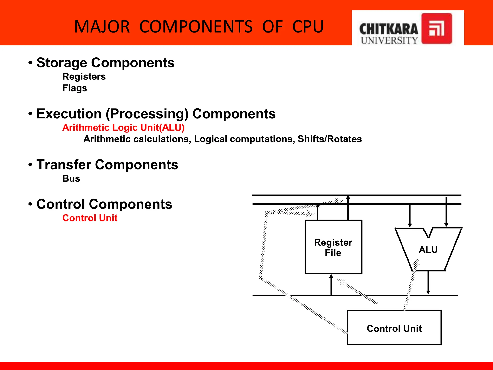
MAJOR COMPONENTS OF CPU
• Storage Components
Registers
Flags
• Execution (Processing) Components
Arithmetic Logic Unit(ALU)
Arithmetic calculations, Logical computations, Shifts/Rotates
• Transfer Components
Bus
• Control Components
Control Unit
Register
File ALU
Control Unit
REGISTERS
• In Basic Computer, there is only one general purpose register, the
Accumulator (AC)
• In modern CPUs, there are many general purpose registers
• It is advantageous to have many registers
– Transfer between registers within the processor are relatively fast
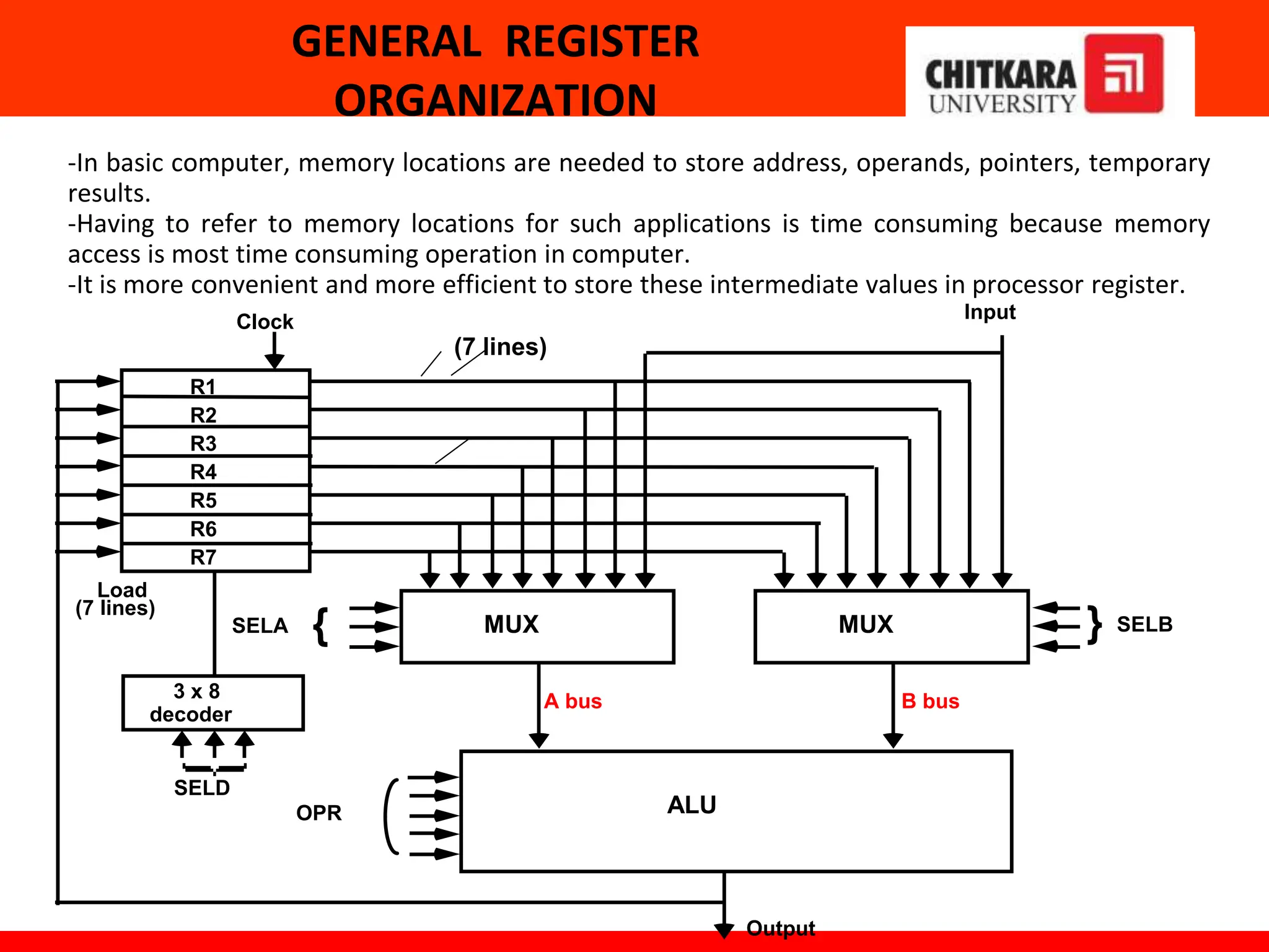
GENERAL REGISTER
ORGANIZATION
MUX
SELA { MUX } SELB
ALU
OPR
R1
R2
R3
R4
R5
R6
R7
Input
3 x 8
decoder
SELD
Load
(7 lines)
Output
A bus B bus
Clock
-In basic computer, memory locations are needed to store address, operands, pointers, temporary
results.
-Having to refer to memory locations for such applications is time consuming because memory
access is most time consuming operation in computer.
-It is more convenient and more efficient to store these intermediate values in processor register.
(7 lines)
OPERATION OF CONTROL UNIT
The control unit :
Directs the information flow through ALU by
- Selecting various Components in the system
- Selecting the Function of ALU
Example: R1  R2 + R3
[1] MUX A selector (SELA): BUS A  R2
[2] MUX B selector (SELB): BUS B  R3
[3] ALU operation selector (OPR): ALU to ADD
[4] Decoder destination selector (SELD): R1  Out Bus
Control Word
Encoding of register selection fields
Binary
Code SELA SELB SELD
000 Input Input None
001 R1 R1 R1
010 R2 R2 R2
011 R3 R3 R3
100 R4 R4 R4
101 R5 R5 R5
110 R6 R6 R6
111 R7 R7 R7
SELA SELB SELD OPR
3 3 3 5
ALU CONTROL-Micro Operations
Encoding of ALU operations OPR
Select Operation Symbol
00000 Transfer A TSFA
00001 Increment A INCA
00010 ADD A + B ADD
00101 Subtract A - B SUB
00110 Decrement A DECA
01000 AND A and B AND
01010 OR A and B OR
01100 XOR A and B XOR
01110 Complement A COMA
10000 Shift right A SHR A
11000 Shift left A SHL A
Examples of ALU Microoperations
Symbolic Designation
Microoperation SELA SELB SELD OPR Control Word
R1 <- R2 - R3 R2 R3 R1 SUB 010 011 001 00101
R4 <- R4 OR R5 R4 R5 R4 OR 100 101 100 01010
R6 <- R6 + 1 R6 - R6 INCA 110 000 110 00001
R7 <- R1 R1 - R7 TSFA 001 000 111 00000
Output <- R2 R2 - None TSFA 010 000 000 00000
Output <- Input Input None TSFA 000 000 000 00000
R4 <- shl R4 R4 - R4 SHLA 100 000 100 11000
R5 <- 0 R5 R5 R5 XOR 101 101 101 01100
REGISTER STACK ORGANIZATION
Register Stack (64 word register stack)
Push, Pop operations ( for insertion and deletion operations)
/* Initially, SP = 0, EMPTY = 1, FULL = 0 */
PUSH POP
SP <- SP + 1 DR <-M[SP]
M[SP] <- DR SP <- SP - 1
If (SP = 0) then (FULL <- 1) If (SP = 0) then (EMPTY <-1)
EMPTY <- 0 FULL <- 0
Stack
- Very useful feature
- Also efficient for arithmetic expression evaluation
- Storage which can be accessed in LIFO
- Pointer: SP
- Only PUSH and POP operations are applicable
A
B
C
0
1
2
3
4
63
Address
FULL EMPTY
SP
DR
Flags
Stack pointer
stack
6 bits
INSTRUCTION FORMAT
OP-code field - specifies the operation to be performed
Address field - designates memory address(es) or a processor register(s)
Mode field - determines how the address field is to be interpreted (to
get effective address or the operand)
• The number of address fields in the instruction format depends on the
internal organization of CPU
• The three most common CPU organizations:
Single accumulator organization:
ADD X /* AC  AC + M[X] */
General register organization:
ADD R1, R2, R3 /* R1  R2 + R3 */
ADD R1, R2 /* R1  R1 + R2 */
MOV R1, R2 /* R1  R2 */
ADD R1, X /* R1  R1 + M[X] */
Stack organization:
PUSH X /* TOS  M[X] */
ADD
• Instruction Fields
• Three-Address Instructions
Program to evaluate X = (A + B) * (C + D) :
ADD R1, A, B /* R1 <- M[A] + M[B] */
ADD R2, C, D /* R2 <- M[C] + M[D] */
MUL X, R1, R2 /* M[X] <- R1 * R2 */
- Results in short programs (Advantage)
- Instruction becomes long (many bits)
• Two-Address Instructions
Program to evaluate X = (A + B) * (C + D) :
MOV R1, A /* R1 <- M[A] */
ADD R1, B /* R1 <- R1 + M[A] */
MOV R2, C /* R2  M[C] */
ADD R2, D /* R2  R2 + M[D] */
MUL R1, R2 /* R1  R1 * R2 */
MOV X, R1 /* M[X]  R1 */
THREE, AND TWO-ADDRESS INSTRUCTIONS
ONE-ADDRESS INSTRUCTIONS (Program)
Zero-ADDRESS INSTRUCTIONS (Program)
Stack Organized
computer uses zero-
address type of
instruction format
and in this type
operand stored in
Push down stack.
Practice Questions
Q. What will be the control word for R4R6 OR
R7?
Q. Write control word for the following micro-
operation: Outputinput.
Q. What contents will be left in stack after executing the
following instructions:
PUSH 10
POP
PUSH 5
PUSH 10
POP
PUSH 15
POP 18
Answer: 5
ADDRESSING MODES
• Addressing Modes
*Specifies a rule for interpreting or modifying the address field of the
instruction (before the operand is actually referenced)
* Variety of addressing modes
- to give programming flexibility to the user
- to use the bits in the address field of the instruction efficiently
TYPES OF ADDRESSING MODES
• Implied Mode
Address of the operands are specified implicitly in the definition of the instruction
- No need to specify address in the instruction
- EA = AC, or EA = Stack[SP]
- Examples from Basic Computer
CLA, CME, INP
• Immediate Mode
Instead of specifying the address of the operand, operand itself is specified
- No need to specify address in the instruction
- However, operand itself needs to be specified
- Sometimes, require more bits than the address
- Fast to acquire an operand
TYPES OF ADDRESSING MODES
• Register Mode
Address specified in the instruction is the register address
- Designated operand need to be in a register
- Shorter address than the memory address
- Saving address field in the instruction
- Faster to acquire an operand than the memory addressing
- EA = IR(R) (IR(R): Register field of IR)
• Register Indirect Mode
Instruction specifies a register which contains the memory address of the operand
- Saving instruction bits since register address
is shorter than the memory address
- Slower to acquire an operand than both the
register addressing or memory addressing
- EA = [IR(R)] ([x]: Content of x)
• Autoincrement or Autodecrement Mode
- When the address in the register is used to access memory, the value in the register
is incremented or decremented by 1 automatically
TYPES OF ADDRESSING MODES
Addressing Modes
• Direct Address Mode
Instruction specifies the memory address which can be used directly to access the
memory
- Faster than the other memory addressing modes
- Too many bits are needed to specify the address for a large physical memory space
- EA = IR(addr) (IR(addr): address field of IR)
• Indirect Addressing Mode
The address field of an instruction specifies the address of a memory location that
contains the address of the operand
- When the abbreviated address is used large physical memory can be addressed with a
relatively small number of bits
- Slow to acquire an operand because of an additional memory access
- EA = M[IR(address)]
TYPES OF ADDRESSING MODES
Addressing Modes
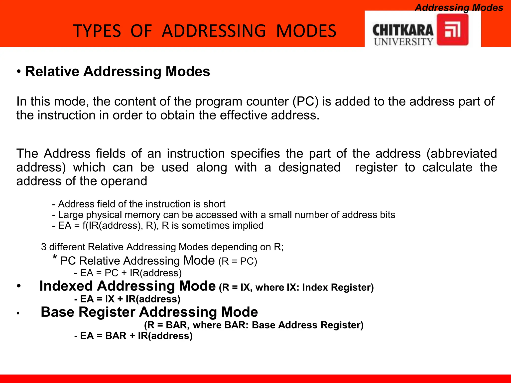
• Relative Addressing Modes
In this mode, the content of the program counter (PC) is added to the address part of
the instruction in order to obtain the effective address.
The Address fields of an instruction specifies the part of the address (abbreviated
address) which can be used along with a designated register to calculate the
address of the operand
- Address field of the instruction is short
- Large physical memory can be accessed with a small number of address bits
- EA = f(IR(address), R), R is sometimes implied
3 different Relative Addressing Modes depending on R;
* PC Relative Addressing Mode (R = PC)
- EA = PC + IR(address)
• Indexed Addressing Mode (R = IX, where IX: Index Register)
- EA = IX + IR(address)
• Base Register Addressing Mode
(R = BAR, where BAR: Base Address Register)
- EA = BAR + IR(address)
ADDRESSING MODES - EXAMPLE
and Practice Question
Addressing
Mode
Effective
Address
Content
of AC
Direct address 500 /* AC  (500) */ 800
Immediate operand 201 /* AC  500 */ 500
Indirect address 800 /* AC  ((500)) */ 300
Relative address 702 /* AC  (PC+500) */ 325
Indexed address 600 /* AC  (RX+500) */ 900
Register - /* AC  R1 */ 400
Register indirect 400 /* AC  (R1) */ 700
Autoincrement 400 /* AC  (R1)+ */ 700
Autodecrement 399 /* AC  -(R) */ 450
Load to AC Mode
Address = 500
Next instruction
200
201
202
399
400
450
700
500 800
600 900
702 325
800 300
Memory
Address
PC = 200
R1 = 400
XR = 100
AC
Practice Question-Cont…
25
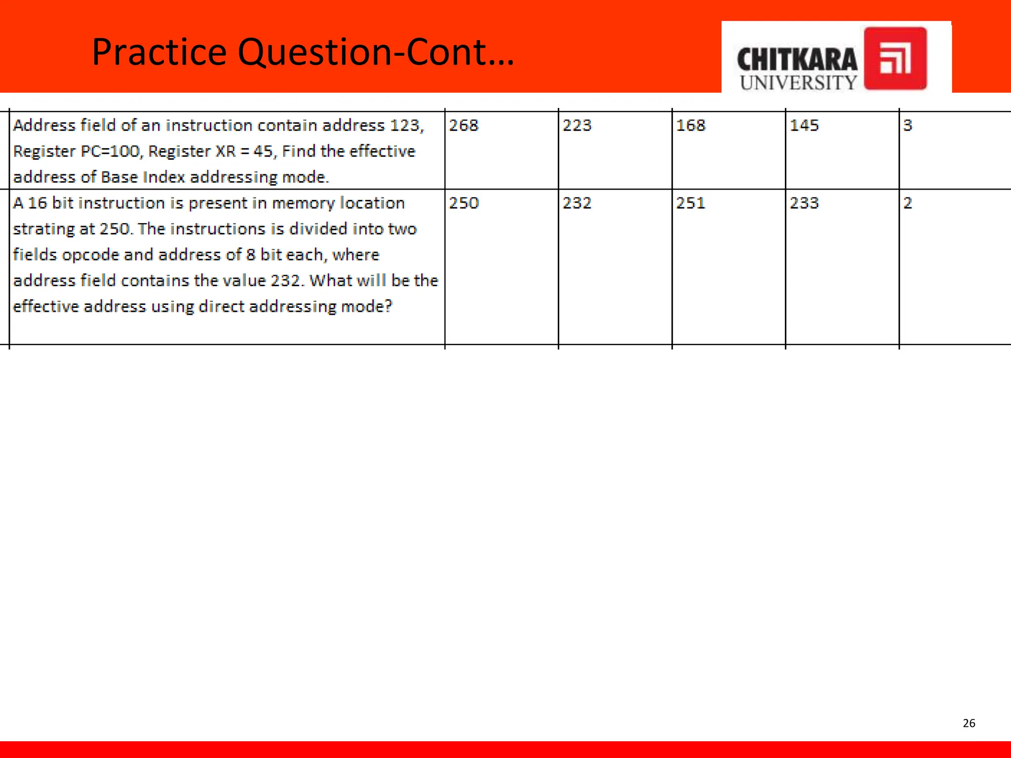
Practice Question-Cont…
26
RISC and CISC
• Reduced Instruction Set Computer (RISC) –
The main idea behind this is to make hardware simpler by using an
instruction set composed of a few basic steps for loading, evaluating, and
storing operations just like a load command will load data, a store
command will store the data.
• Complex Instruction Set Computer (CISC) –
The main idea is that a single instruction will do all loading, evaluating,
and storing operations just like a multiplication command will do stuff
like loading data, evaluating, and storing it, hence it’s complex.
27
Continue..
28
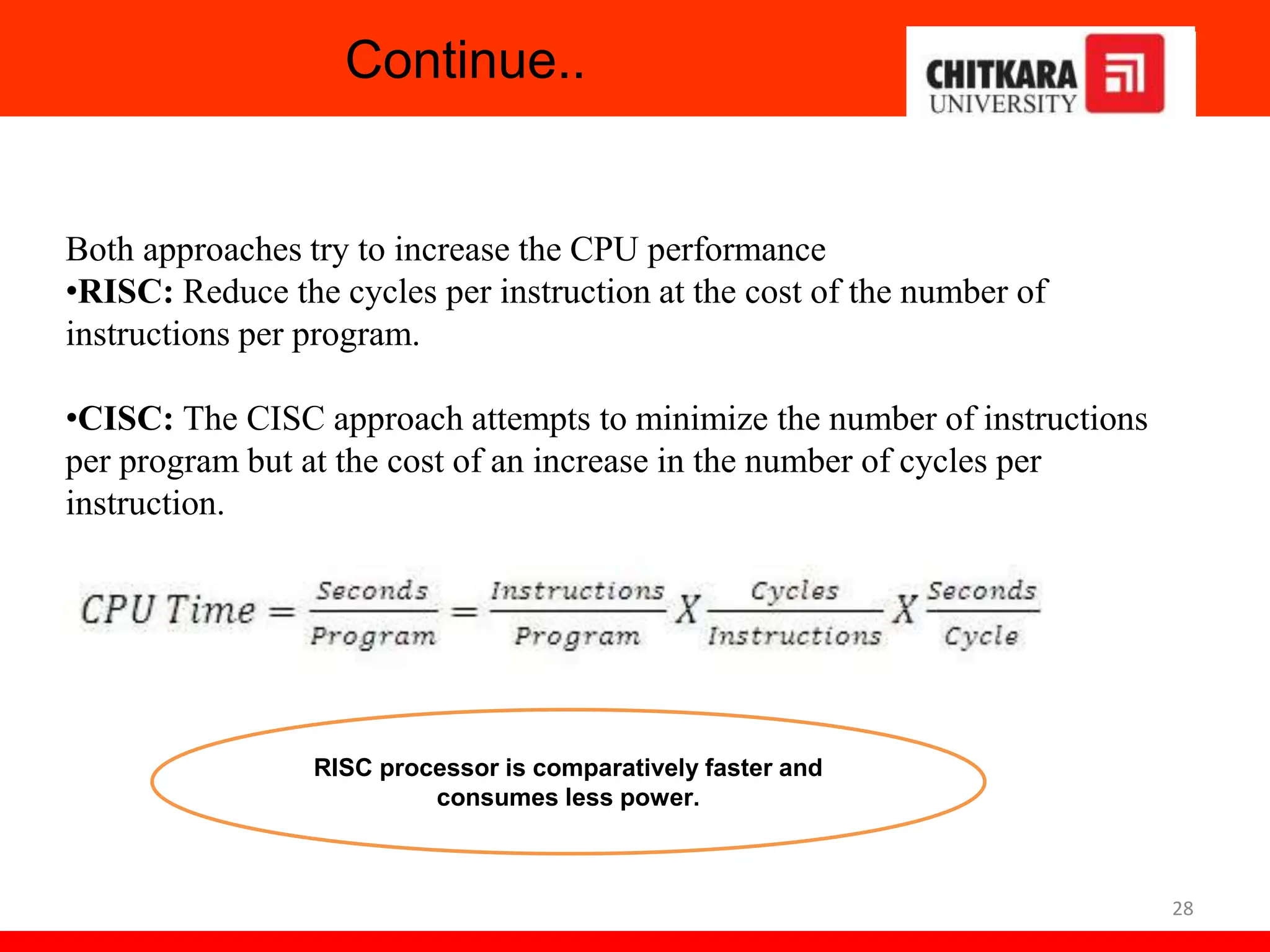
Both approaches try to increase the CPU performance
•RISC: Reduce the cycles per instruction at the cost of the number of
instructions per program.
•CISC: The CISC approach attempts to minimize the number of instructions
per program but at the cost of an increase in the number of cycles per
instruction.
RISC processor is comparatively faster and
consumes less power.
Characteristic of RISC
29
Earlier when programming was done using assembly language, a need
was felt to make instruction do more tasks because programming in
assembly was tedious and error-prone due to which CISC architecture
evolved but with the uprise of high-level language dependency on
assembly reduced RISC architecture prevailed.
Characteristic of RISC –
1.Simpler instruction, hence simple instruction decoding.
2.Instruction comes in the size of one word.
3.Instruction takes a single clock cycle to get executed.
4.More general-purpose registers.
5.Simple Addressing Modes.
6.Fewer Data types.
7.A pipeline can be achieved.
Characteristic of CISC
30
Characteristic of CISC –
1.Complex instruction, hence complex instruction decoding.
2.Instructions are larger than one-word size.
3.Instruction may take more than a single clock cycle to get executed.
4.Less number of general-purpose registers as operations get
performed in memory itself.
5.Complex Addressing Modes.
6.More Data types.
CISC is a processor which is developed with a full (complex)
set of instructions aimed at providing the full processor
capacity in the most efficient manner.
Continue..
31
Example – Suppose we have to add two 8-bit numbers:
•CISC approach: There will be a single command or instruction for this like
ADD which will perform the task.
•RISC approach: Here programmer will write the first load command to load
data in registers then it will use a suitable operator and then it will store the
result in the desired location.
So, add operation is divided into parts i.e. load, operate, store due to which
RISC programs are longer and require more memory to get stored but
require fewer transistors due to less complex command.
Difference
32
RISC CISC
Focus on software Focus on hardware
Uses only Hardwired control unit
Uses both hardwired and microprogrammed
control unit
Transistors are used for more registers
Transistors are used for storing complex
Instructions
Fixed sized instructions Variable sized instructions
Can perform only Register to Register
Arithmetic operations
Can perform REG to REG or REG to MEM or
MEM to MEM
Requires more number of registers Requires less number of registers
Code size is large Code size is small
An instruction executed in a single clock cycle Instruction takes more than one clock cycle
An instruction fit in one word Instructions are larger than the size of one word
Parallel Processing
33
34
Parallel Processing
• Parallel processing can be described as a class of techniques which enables the
system to achieve simultaneous data-processing tasks to increase the
computational speed of a computer system.
• The primary purpose of parallel processing is to speed up the computer processing
capability and increase its throughput, i.e. the amount of processing that can be
accomplished during a given interval of time.
• A parallel processing system is able to perform concurrent data processing to
achieve faster execution time. For example, while an instruction is being executed
in the ALU, the next instruction can be read from memory.
35
Parallel Processing
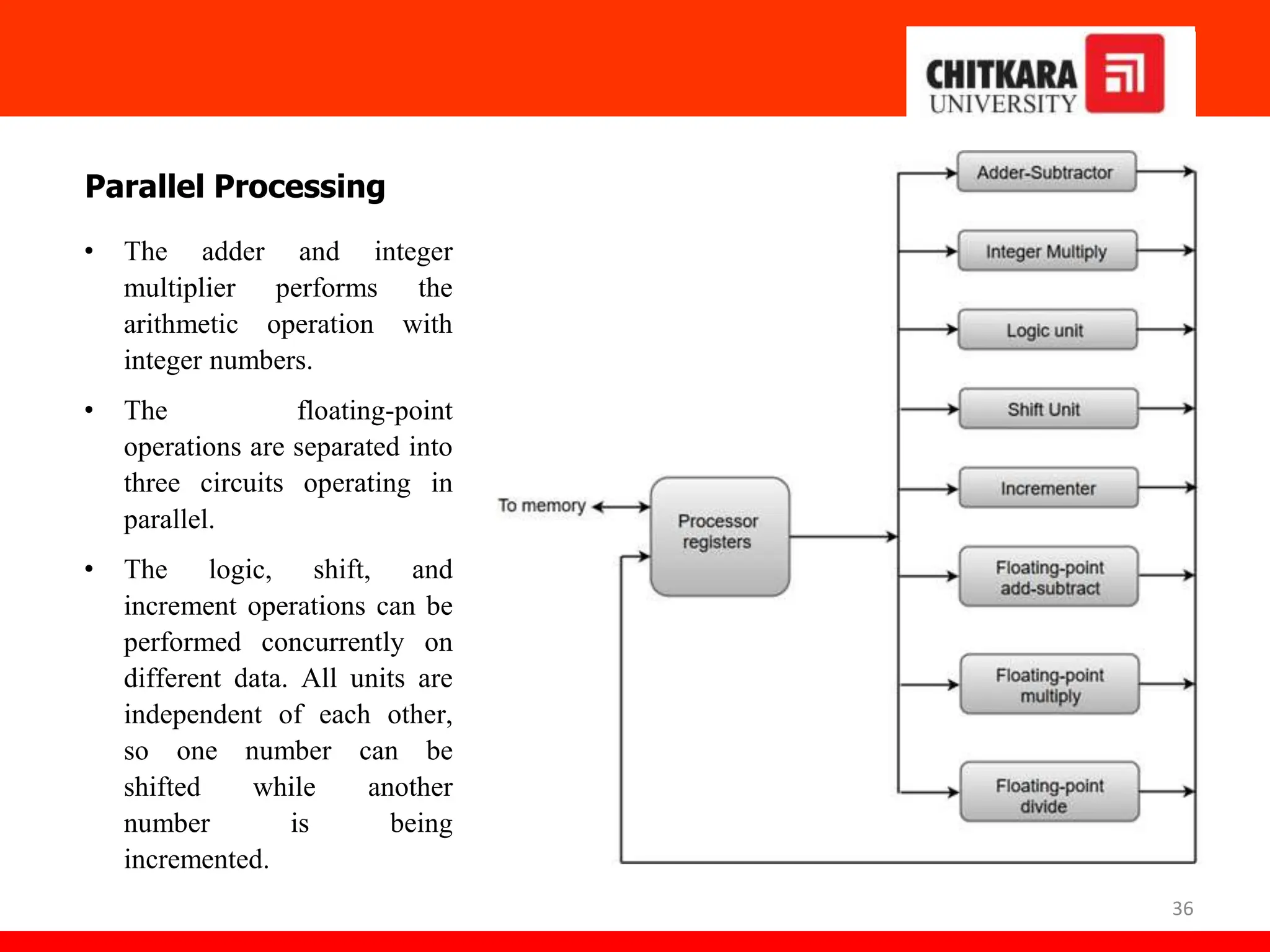
The following diagram shows one possible way of separating the execution unit into
eight functional units operating in parallel.
The operation performed in each functional unit is indicated in each block of the
diagram:
36
Parallel Processing
• The adder and integer
multiplier performs the
arithmetic operation with
integer numbers.
• The floating-point
operations are separated into
three circuits operating in
parallel.
• The logic, shift, and
increment operations can be
performed concurrently on
different data. All units are
independent of each other,
so one number can be
shifted while another
number is being
incremented.
37
Flynn's Classification of Computers
M.J. Flynn proposed a classification for the organization of a computer system by the
number of instructions and data items that are manipulated simultaneously.
• The sequence of instructions read from memory constitutes an instruction
stream.
• The operations performed on the data in the processor constitute a data stream.
• Parallel processing may occur in the instruction stream, in the data stream, or
both.
Flynn's classification divides computers into four major groups that are:
1. Single instruction stream, single data stream (SISD)
2. Single instruction stream, multiple data stream (SIMD)
3. Multiple instruction stream, single data stream (MISD)
4. Multiple instruction stream, multiple data stream (MIMD)
38
Flynn's Classification of Computers
SISD stands for 'Single Instruction and Single Data Stream'. It represents the
organization of a single computer containing a control unit, a processor unit, and a
memory unit.
Most conventional computers have SISD architecture like the traditional Von-
Neumann computers.
Where, CU = Control Unit,
PE = Processing Element,
M = Memory
Instructions are decoded by the
Control Unit and then the Control
Unit sends the instructions to the
processing units for execution.
39
Flynn's Classification of Computers - SIMD
SIMD stands for 'Single Instruction and
Multiple Data Stream'. It represents an
organization that includes many processing
units under the supervision of a common
control unit.
All processors receive the same instruction
from the control unit but operate on different
items of data. The shared memory unit must
contain multiple modules so that it can
communicate with all the processors
simultaneously.
SIMD is mainly dedicated to array
processing machines. However,
vector processors can also be seen as a
part of this group.
40
Flynn's Classification of Computers
MISD stands for 'Multiple Instruction and Single Data stream'.
MISD structure is only of theoretical interest since no practical system has been
constructed using this organization.
In MISD, multiple processing units operate on one single-data stream. Each
processing unit operates on the data independently via separate instruction stream.
41
Flynn's Classification of Computers
MIMD stands for 'Multiple Instruction and Multiple Data Stream'.
In this organization, all processors in a parallel computer can execute different
instructions and operate on various data at the same time.
In MIMD, each processor has a separate program and an instruction stream is
generated from each program.
Example:
Cray T90, Cray T3E, IBM-SP2
Pipelining
42
43
Pipelining
• The term Pipelining refers to a technique of decomposing a sequential process
into sub-operations, with each sub-operation being executed in a dedicated
segment that operates concurrently with all other segments.
• The most important characteristic of a pipeline technique is that several
computations can be in progress in distinct segments at the same time.
• The overlapping of computation is made possible by associating a register with
each segment in the pipeline. The registers provide isolation between each
segment so that each can operate on distinct data simultaneously.
• The structure of a pipeline organization can be represented simply by including an
input register for each segment followed by a combinational circuit.
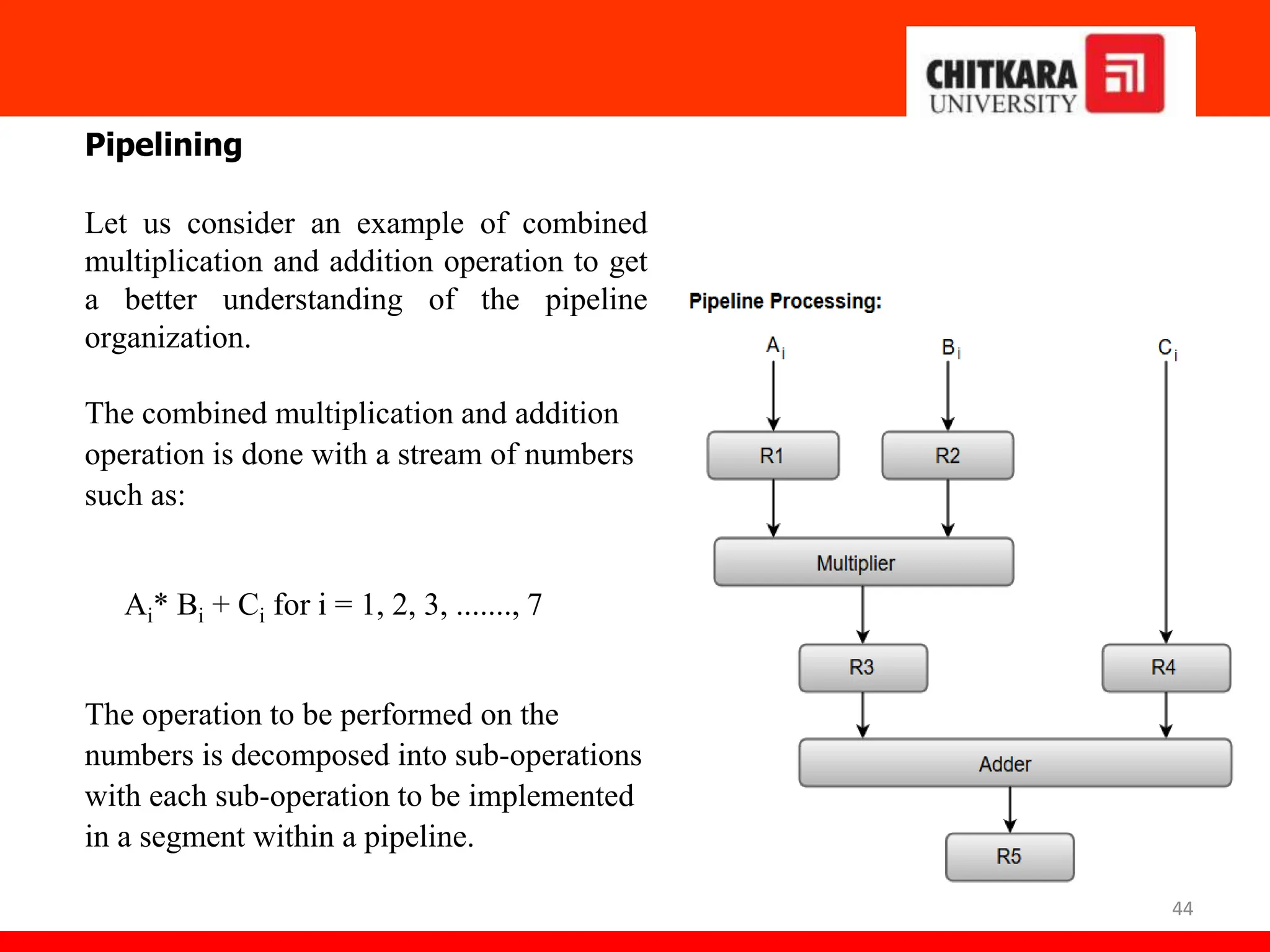
44
Pipelining
Let us consider an example of combined
multiplication and addition operation to get
a better understanding of the pipeline
organization.
The combined multiplication and addition
operation is done with a stream of numbers
such as:
Ai* Bi + Ci for i = 1, 2, 3, ......., 7
The operation to be performed on the
numbers is decomposed into sub-operations
with each sub-operation to be implemented
in a segment within a pipeline.
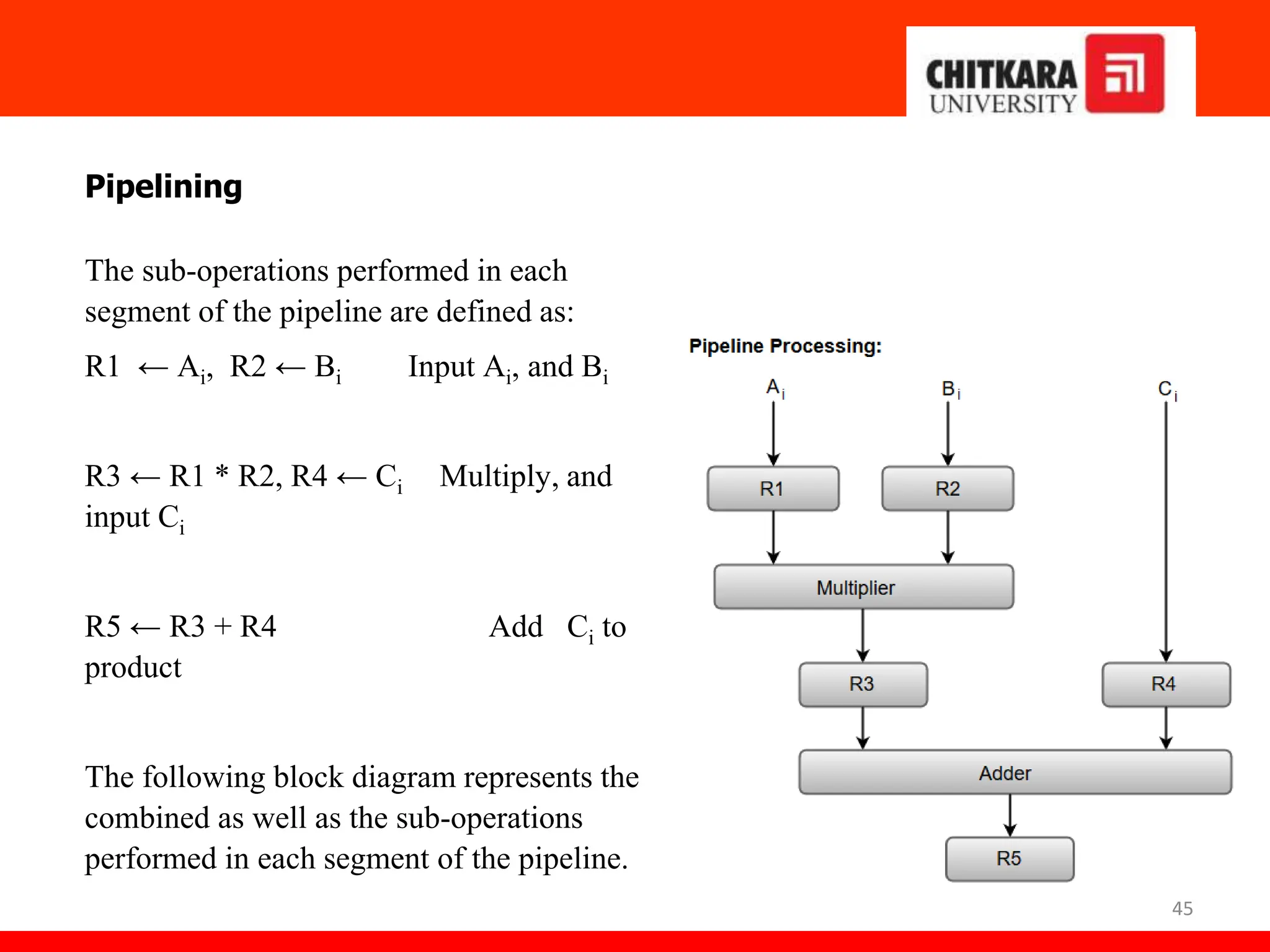
45
Pipelining
The sub-operations performed in each
segment of the pipeline are defined as:
R1 ← Ai, R2 ← Bi Input Ai, and Bi
R3 ← R1 * R2, R4 ← Ci Multiply, and
input Ci
R5 ← R3 + R4 Add Ci to
product
The following block diagram represents the
combined as well as the sub-operations
performed in each segment of the pipeline.
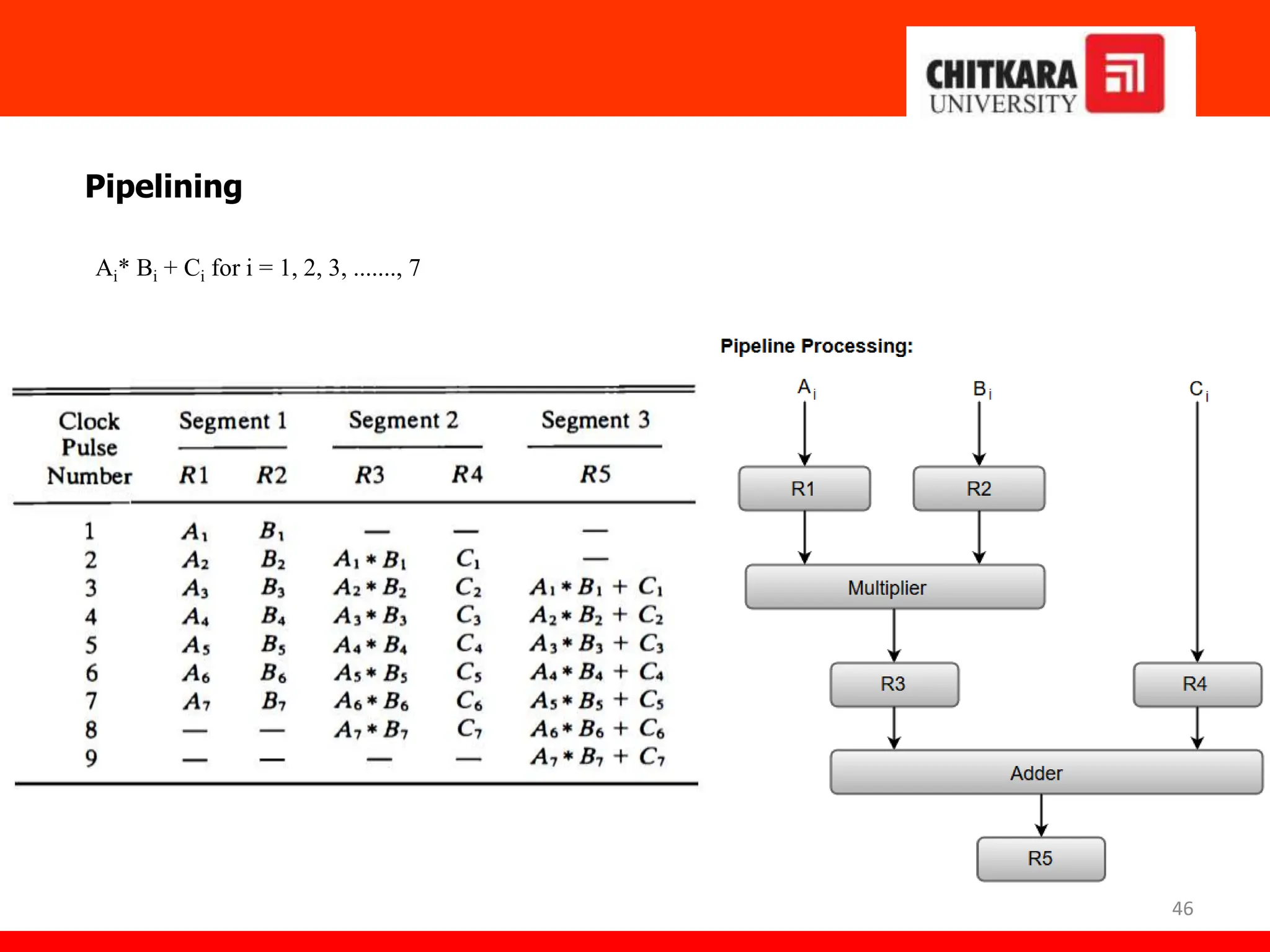
46
Pipelining
Ai* Bi + Ci for i = 1, 2, 3, ......., 7
47
Pipelining
In general, the pipeline organization is applicable for two areas of computer design
which includes:
1. Arithmetic Pipeline
2. Instruction Pipeline
48
Pipelining
Arithmetic Pipeline
• Arithmetic Pipelines are mostly used in high-speed computers.
• They are used to implement floating-point operations, multiplication of fixed-point
numbers, and similar computations encountered in scientific problems.
To understand the concepts of arithmetic pipeline in a more convenient way, let us consider
an example of a pipeline unit for floating-point addition and subtraction.
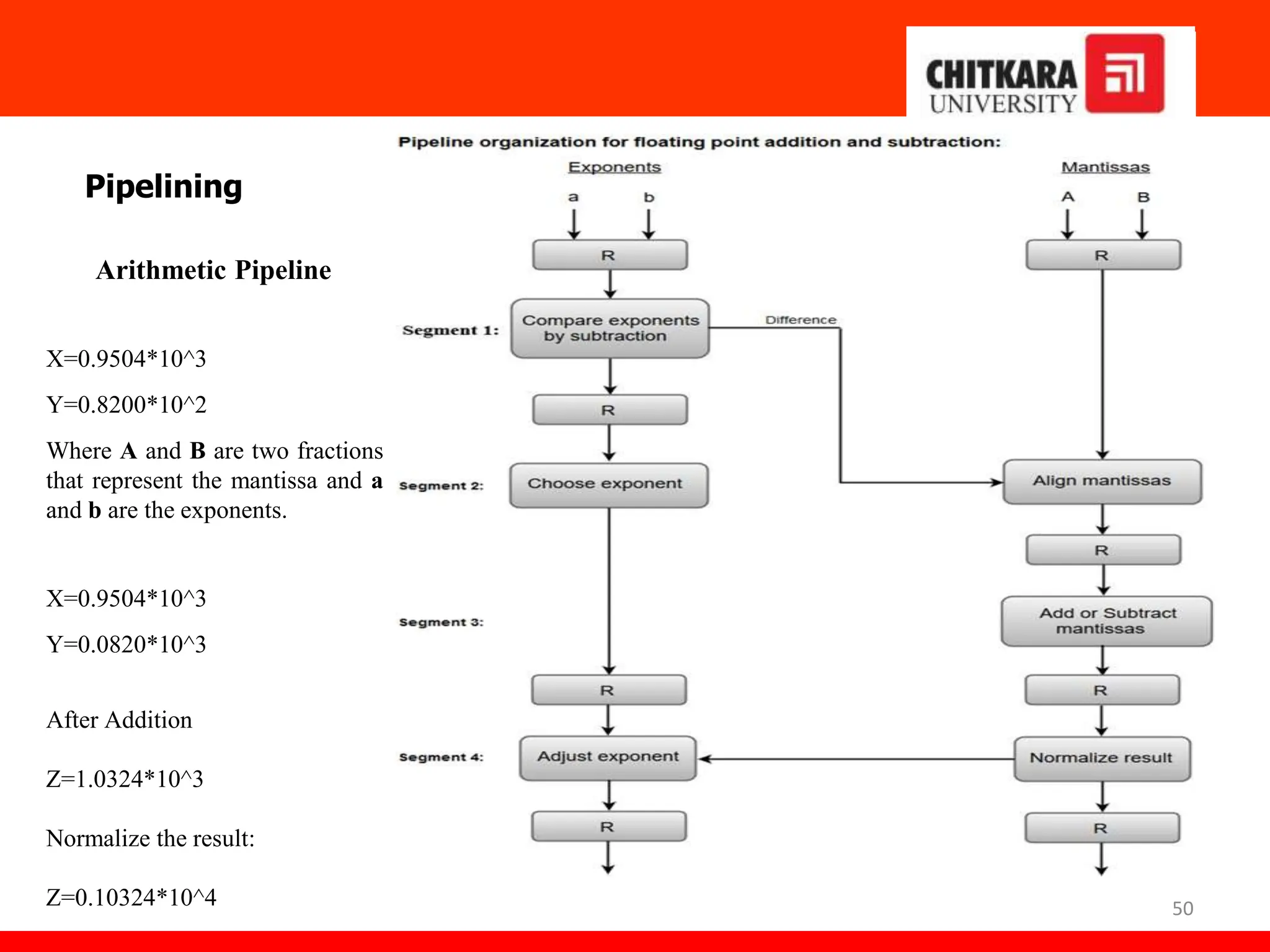
The inputs to the floating-point adder pipeline are two normalized floating-point binary
numbers defined as:
X=A*2^a=0.9504*10^3
Y=B*2^a=0.8200*10^2
Where A and B are two fractions that represent the mantissa and a and b are the exponents.
49
Pipelining
Arithmetic Pipeline
The combined operation of floating-point addition and subtraction is divided into
four segments. Each segment contains the corresponding suboperation to be
performed in the given pipeline. The suboperations that are shown in the four
segments are:
1. Compare the exponents by subtraction.
2. Align the mantissas.
3. Add or subtract the mantissas.
4. Normalize the result.
50
Pipelining
Arithmetic Pipeline
X=0.9504*10^3
Y=0.8200*10^2
Where A and B are two fractions
that represent the mantissa and a
and b are the exponents.
X=0.9504*10^3
Y=0.0820*10^3
After Addition
Z=1.0324*10^3
Normalize the result:
Z=0.10324*10^4
51
Pipelining
Instruction Pipeline
• Pipeline processing can occur not only in the data stream but in the instruction
stream as well.
• Most of the digital computers with complex instructions require instruction
pipeline to carry out operations like fetch, decode and execute instructions.
In general, the computer needs to process each instruction with the following
sequence of steps.
1. Fetch instruction from memory.
2. Decode the instruction.
3. Calculate the effective address.
4. Fetch the operands from memory.
5. Execute the instruction.
6. Store the result in the proper place.
52
Pipelining
Instruction Pipeline
Each step is executed in a particular segment, and there are times when different
segments may take different times to operate on the incoming information.
Moreover, there are times when two or more segments may require memory
access at the same time, causing one segment to wait until another is finished with
the memory.
The organization of an instruction pipeline will be more efficient if the instruction
cycle is divided into segments of equal duration. One of the most common
examples of this type of organization is a Four-segment instruction pipeline.
53
Pipelining
Instruction Pipeline
• A four-segment instruction pipeline combines two or more different segments
and makes it as a single one.
• For instance, the decoding of the instruction can be combined with the
calculation of the effective address into one segment.
The following block diagram (next slide) shows a typical example of a four-
segment instruction pipeline. The instruction cycle is completed in four segments.
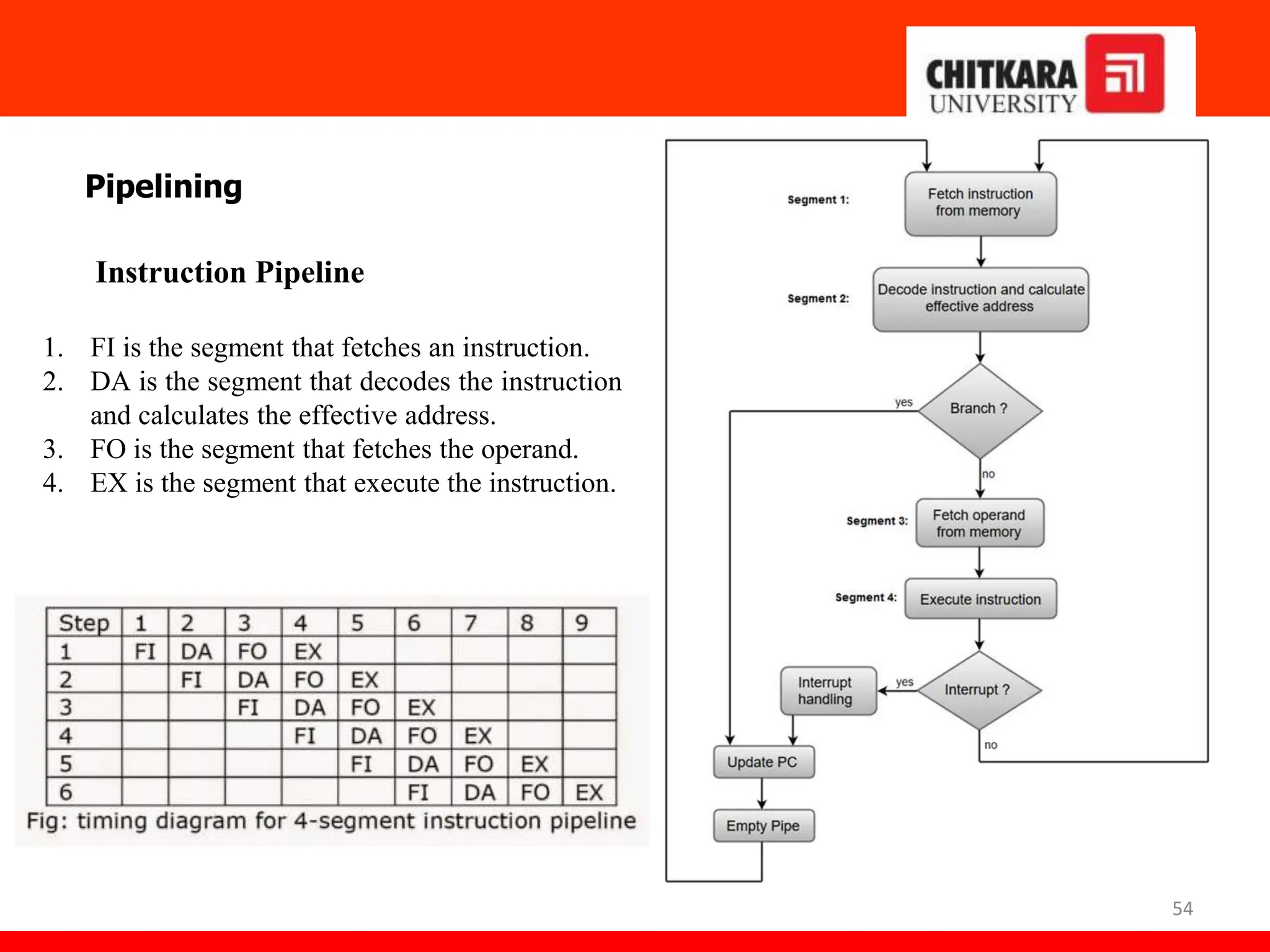
Segment 1: The instruction fetch segment can be implemented using first in, first
out (FIFO) buffer.
Segment 2: The instruction fetched from memory is decoded in the second
segment, and eventually, the effective address is calculated in a separate
arithmetic circuit.
Segment 3: An operand from memory is fetched in the third segment.
Segment 4: The instructions are finally executed in the last segment of the
pipeline organization.
54
Pipelining
Instruction Pipeline
1. FI is the segment that fetches an instruction.
2. DA is the segment that decodes the instruction
and calculates the effective address.
3. FO is the segment that fetches the operand.
4. EX is the segment that execute the instruction.
55
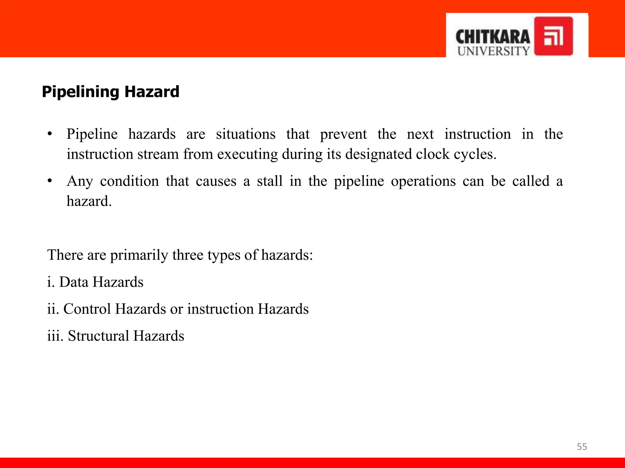
Pipelining Hazard
• Pipeline hazards are situations that prevent the next instruction in the
instruction stream from executing during its designated clock cycles.
• Any condition that causes a stall in the pipeline operations can be called a
hazard.
There are primarily three types of hazards:
i. Data Hazards
ii. Control Hazards or instruction Hazards
iii. Structural Hazards
56
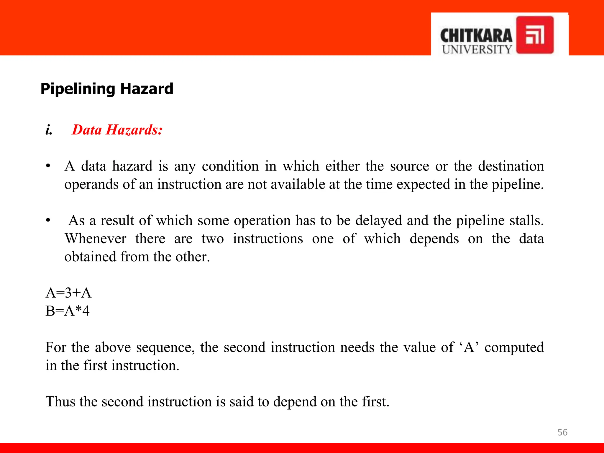
Pipelining Hazard
i. Data Hazards:
• A data hazard is any condition in which either the source or the destination
operands of an instruction are not available at the time expected in the pipeline.
• As a result of which some operation has to be delayed and the pipeline stalls.
Whenever there are two instructions one of which depends on the data
obtained from the other.
A=3+A
B=A*4
For the above sequence, the second instruction needs the value of ‘A’ computed
in the first instruction.
Thus the second instruction is said to depend on the first.
57
Pipelining Hazard
ii. Structural Hazards:
• This situation arises mainly when two instructions require a given hardware
resource at the same time and hence for one of the instructions the pipeline
needs to be delayed.
• The most common case is when memory is accessed at the same time by two
instructions. One instruction may need to access the memory as part of the
Execute or Write back phase while other instruction is being fetched.
• In this case if both the instructions and data reside in the same memory. Both
the instructions can’t proceed together and one of them needs to be stalled till
the other is done with the memory access part.
• Thus in general, sufficient hardware resources are needed for avoiding
structural hazards.
58
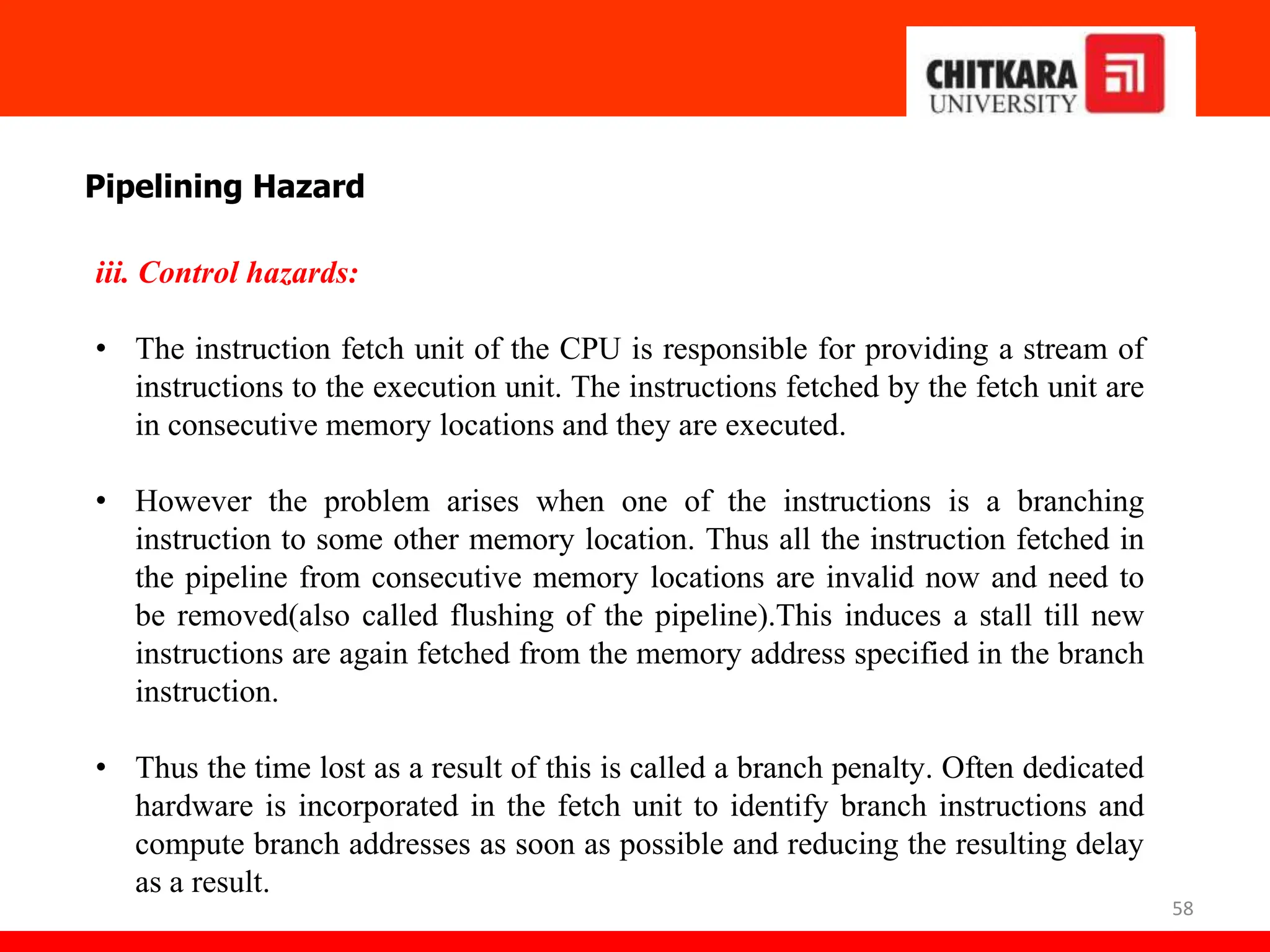
Pipelining Hazard
iii. Control hazards:
• The instruction fetch unit of the CPU is responsible for providing a stream of
instructions to the execution unit. The instructions fetched by the fetch unit are
in consecutive memory locations and they are executed.
• However the problem arises when one of the instructions is a branching
instruction to some other memory location. Thus all the instruction fetched in
the pipeline from consecutive memory locations are invalid now and need to
be removed(also called flushing of the pipeline).This induces a stall till new
instructions are again fetched from the memory address specified in the branch
instruction.
• Thus the time lost as a result of this is called a branch penalty. Often dedicated
hardware is incorporated in the fetch unit to identify branch instructions and
compute branch addresses as soon as possible and reducing the resulting delay
as a result.
Direct Memory Access (DMA)
59
60
Direct Memory Access (DMA)
• The transfer of data between a fast storage device such as magnetic disk and
memory is often limited by the speed of the CPU.
• Removing CPU from the path and letting the I/O devices manage the memory
buses directly would improve the speed of transfer.
• This transfer technique is called direct memory access (DMA).
• During DMA transfer, the CPU is idle and has no control of the memory buses.
• A DMA controller takes over the buses to manage the transfer directly the I/O
device and memory.
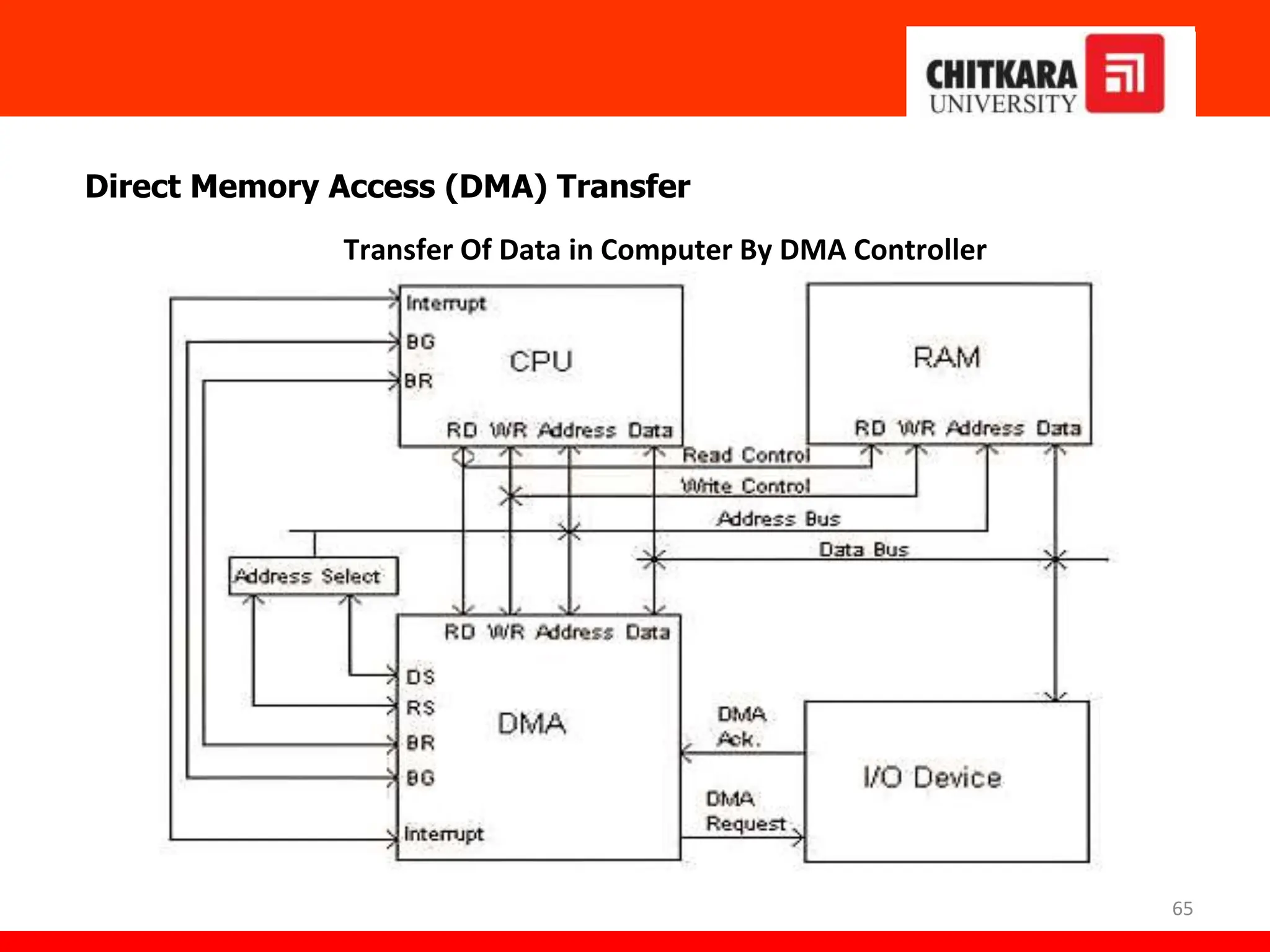
61
Direct Memory Access (DMA)
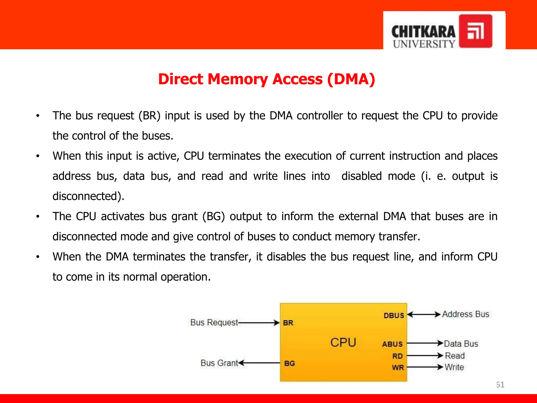
• The bus request (BR) input is used by the DMA controller to request the CPU to provide
the control of the buses.
• When this input is active, CPU terminates the execution of current instruction and places
address bus, data bus, and read and write lines into disabled mode (i. e. output is
disconnected).
• The CPU activates bus grant (BG) output to inform the external DMA that buses are in
disconnected mode and give control of buses to conduct memory transfer.
• When the DMA terminates the transfer, it disables the bus request line, and inform CPU
to come in its normal operation.
62
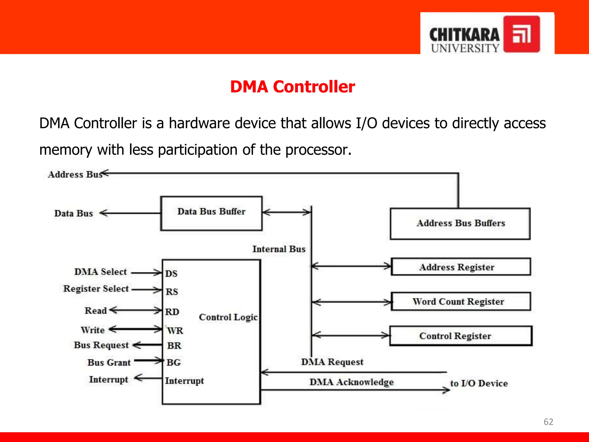
DMA Controller
DMA Controller is a hardware device that allows I/O devices to directly access
memory with less participation of the processor.
63
Direct Memory Access (DMA) Transfer
• DMA controller has to share the bus with the processor to make the data transfer. The device
that holds the bus at a given time is called bus master.
• When a transfer from I/O device to the memory or vice verse has to be made, the processor
stops the execution of the current program, increments the program counter, moves data
over stack then sends a DMA select signal to DMA controller over the address bus.
• If the DMA controller is free, it requests the control of bus from the processor by raising the
bus request signal. Processor grants the bus to the controller by raising the bus grant signal,
now DMA controller is the bus master.
• The processor initiates the DMA controller by sending the memory addresses, number of
blocks of data to be transferred and direction of data transfer.
• After assigning the data transfer task to the DMA controller, instead of waiting ideally till
completion of data transfer, the processor resumes the execution of the program after
retrieving instructions from the stack.
.
64
Direct Memory Access (DMA) Transfer
• DMA controller now has the full control of buses and can interact directly with memory and
I/O devices independent of CPU. It makes the data transfer according to the control
instructions received by the processor.
• After completion of data transfer, it disables the bus request signal and CPU disables the bus
grant signal thereby moving control of buses to the CPU.
• When an I/O device wants to initiate the transfer then it sends a DMA request signal to the
DMA controller, for which the controller acknowledges if it is free.
• Then the controller requests the processor for the bus, raising the bus request signal. After
receiving the bus grant signal it transfers the data from the device. For n channeled DMA
controller n number of external devices can be connected.
65
Direct Memory Access (DMA) Transfer
Transfer Of Data in Computer By DMA Controller
66
Direct Memory Access (DMA) Transfer
The DMA transfers the data in three modes which include the following
a) Burst Mode: In this mode DMA handover the buses to CPU only after
completion of whole data transfer. Meanwhile, if the CPU requires the bus it has
to stay ideal and wait for data transfer.
b) Cycle Stealing Mode: In this mode, DMA gives control of buses to CPU after
transfer of every byte. It continuously issues a request for bus control, makes the
transfer of one byte and returns the bus. By this CPU doesn’t have to wait for a long
time if it needs a bus for higher priority task.
c) Transparent Mode: Here, DMA transfers data only when CPU is executing the
instruction which does not require the use of buses.
Input Output Processors (IOP)
67
68
Input Output Processors (IOP)
• The DMA mode of data transfer reduces CPU’s overhead in handling
I/O operations. It also allows parallelism in CPU and I/O operations.
• Such parallelism is necessary to avoid wastage of valuable CPU time
while handling I/O devices whose speeds are much slower as
compared to CPU.
• The concept of DMA operation can be extended to relieve the CPU
further from getting involved with the execution of I/O operations.
• This gives rises to the development of special purpose processor
called Input-Output Processor (IOP).
• The Input Output Processor (IOP) is just like a CPU that handles the
details of I/O operations.
• It is more equipped with facilities than those are available in typical
DMA controller.
• The IOP can fetch and execute its own instructions that are
specifically designed to characterize I/O transfers.
• In addition to the I/O – related tasks, it can perform other processing
tasks like arithmetic, logic, branching and code translation.
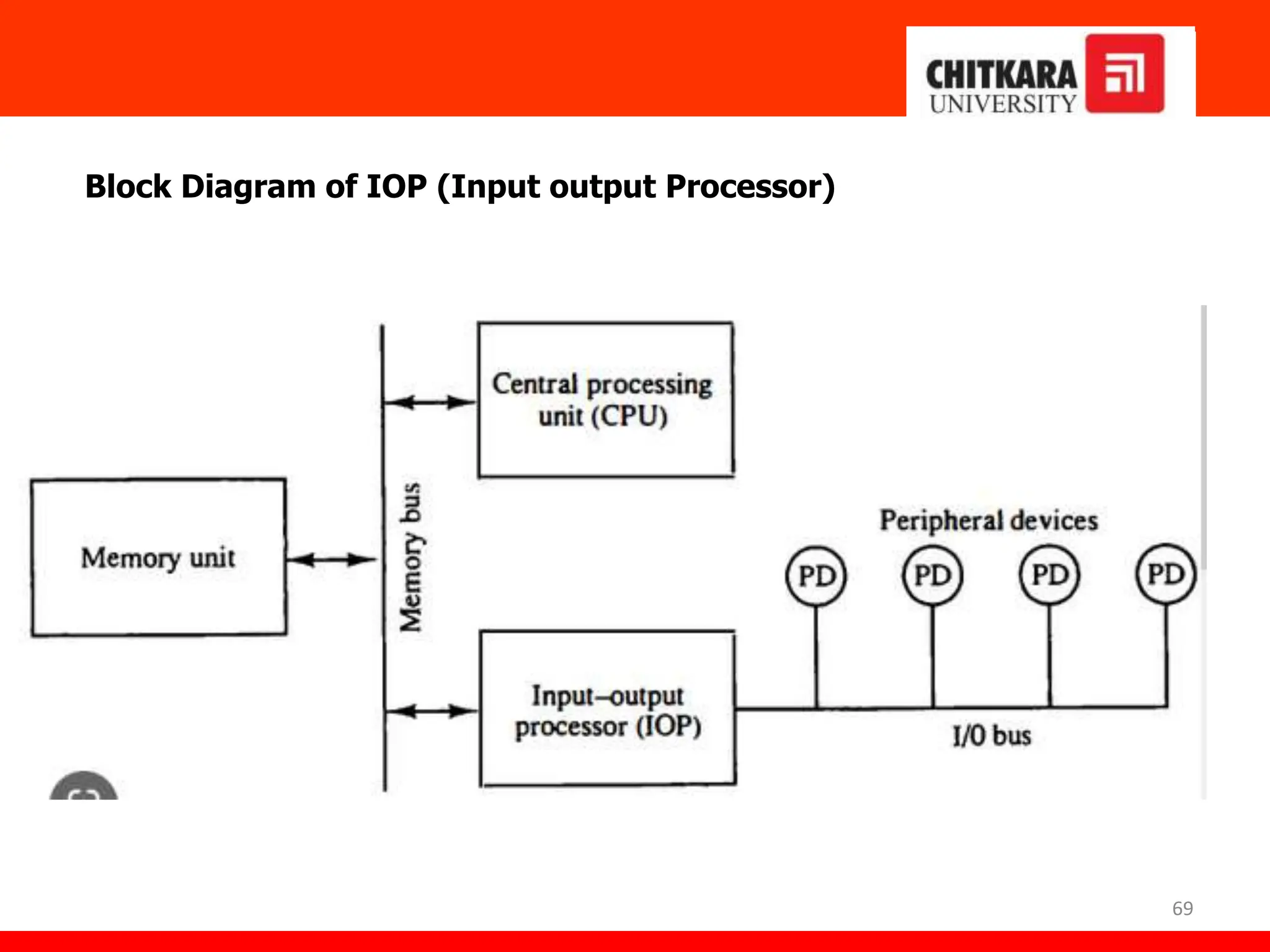
69
Block Diagram of IOP (Input output Processor)
70
IOP
• The Input Output Processor is a specialized processor which loads and stores data
into memory along with the execution of I/O instructions.
• It acts as an interface between system and devices. It involves a sequence of events
to executing I/O operations and then store the results into the memory.
Advantages –
•The I/O devices can directly access the main memory without the intervention by the
processor in I/O processor based systems.
•It is used to address the problems that are arises in Direct memory access method.
•Reduced processor workload: With an I/O processor, the main processor doesn’t
have to deal with I/O operations, allowing it to focus on other tasks. This results in more
efficient use of the processor’s resources and can lead to faster overall system
performance.
• Improved data transfer rates: Since the I/O processor can access memory directly,
data transfers between I/O devices and memory can be faster and more efficient than
with other methods.
• Scalability: I/O processor based systems can be designed to scale easily, allowing
for additional I/O processors to be added as needed. This can be particularly useful in
large-scale data centers or other environments where the number of I/O devices is
constantly changing.
71
Disadvantages of IOP
Disadvantages –
1.Cost: I/O processors can add significant cost to a system due to the additional
hardware and complexity required. This can be a barrier to adoption, especially for
smaller systems.
2.Increased complexity: The addition of an I/O processor can increase the overall
complexity of a system, making it more difficult to design, build, and maintain. This
can also make it harder to diagnose and troubleshoot issues.
3.Limited performance gains: While I/O processors can improve system
performance by offloading I/O tasks from the main processor, the gains may not be
significant in all cases. In some cases, the additional overhead of the I/O processor
may actually slow down the system.
4.Synchronization issues: With multiple processors accessing the same memory,
synchronization issues can arise, leading to potential data corruption or other
errors.
72
IOP –CPU Communication
73
IOP-CPU Communication
• There is a communication channel between IOP and CPU to perform task
which come under computer architecture.
• This channel explains the commands executed by IOP and CPU while
performing some programs.
• The CPU do not executes the instructions but it assigns the task of initiating
operations, the instructions are executed by IOP.
• I/O transfer is instructed by CPU. The IOP asks for CPU through interrupt.
• This channel starts by CPU, by giving “test IOP path” instruction to IOP and
then the communication begins
• IOP and CPU Whenever CPU gets interrupt from IOP to access
memory, it sends test path instruction to IOP.
• IOP executes and check for status, if the status given to CPU is OK,
then CPU gives start instruction to IOP and gives it some control and
get back to some another (or same) program, after that IOP is able to
access memory for its program.
74
Thank You

Unit 4_DECA_Complete Digital Electronics.pptx

  • 1.
    1 Digital Electronics andComputer Architecture (DECA) CPU and its Organization (Unit-4): (Complete Unit) Central Processing Unit: Introduction, General Register Organization, Operation of Control Unit, Control Word, Stack Organization and Instruction Format, Various Addressing Modes, RISC and CISC Characteristics, Introduction to Parallel Processing, Flynn’s Classification of Computers, Pipelining, Pipeline Hazards, Direct Memory Access (DMA), DMA Transfer, Input-Output Processor (IOP) B.E.-CSE 1st Sem. Department of Interdisciplinary Courses in Engineering (DICE) & Department of Computer Science and Engineering
  • 2.
    2 Central Processing Unit(CPU) CPU is the brain of the computer. All types of data processing operations and all the important functions of a computer are performed by the CPU. The CPU consists of 3 major units, which are: 1. Memory or Storage Unit 2. Control Unit 3. ALU(Arithmetic Logic Unit) Central Processing Unit (CPU)
  • 3.
    3 The part ofthe computer that performs the bulk of data-processing operations is called the central processing unit (CPU). The CPU is made up of three major parts : Register set, Control Unit and Arithmetic Logical Unit (ALU). The register set stores intermediate data used during the execution of instructions. The ALU performs the required micro-operations for executing the instructions. The control unit generates the sequence of various micro-operations, supervises the transfer of information among the registers and instructs the ALU as to which operation to perform. Central Processing Unit (CPU)
  • 4.
  • 5.
    5 Central Processing Unit(Cont..) Memory or Storage Unit:  Data and instructions are stored in memory units which are required for processing.  It also stores the intermediate results of any calculation or task when they are in process.  The final results of processing are stored in the memory units before these results are released to an output device for giving the output to the user.  All sorts of inputs and outputs are transmitted through the memory unit.
  • 6.
    6 Central Processing Unit(Cont..) Control Unit:  Controlling of data and transfer of data and instructions is done by the control unit among other parts of the computer.  The control unit is responsible for managing all the units of the computer.  The main task of the control unit is to obtain the instructions or data which is input from the memory unit, interprets them, and then directs the operation of the computer according to that.  The control unit is responsible for communication with Input and output devices for the transfer of data or results from memory.  The control unit is not responsible for the processing of data or storing data.
  • 7.
    7 Central Processing Unit(Cont..) ALU (Arithmetic Logic Unit) :  Arithmetic Section  Logic Section
  • 8.
    MAJOR COMPONENTS OFCPU • Storage Components Registers Flags • Execution (Processing) Components Arithmetic Logic Unit(ALU) Arithmetic calculations, Logical computations, Shifts/Rotates • Transfer Components Bus • Control Components Control Unit Register File ALU Control Unit
  • 9.
    REGISTERS • In BasicComputer, there is only one general purpose register, the Accumulator (AC) • In modern CPUs, there are many general purpose registers • It is advantageous to have many registers – Transfer between registers within the processor are relatively fast
  • 10.
    GENERAL REGISTER ORGANIZATION MUX SELA {MUX } SELB ALU OPR R1 R2 R3 R4 R5 R6 R7 Input 3 x 8 decoder SELD Load (7 lines) Output A bus B bus Clock -In basic computer, memory locations are needed to store address, operands, pointers, temporary results. -Having to refer to memory locations for such applications is time consuming because memory access is most time consuming operation in computer. -It is more convenient and more efficient to store these intermediate values in processor register. (7 lines)
  • 11.
    OPERATION OF CONTROLUNIT The control unit : Directs the information flow through ALU by - Selecting various Components in the system - Selecting the Function of ALU Example: R1  R2 + R3 [1] MUX A selector (SELA): BUS A  R2 [2] MUX B selector (SELB): BUS B  R3 [3] ALU operation selector (OPR): ALU to ADD [4] Decoder destination selector (SELD): R1  Out Bus Control Word Encoding of register selection fields Binary Code SELA SELB SELD 000 Input Input None 001 R1 R1 R1 010 R2 R2 R2 011 R3 R3 R3 100 R4 R4 R4 101 R5 R5 R5 110 R6 R6 R6 111 R7 R7 R7 SELA SELB SELD OPR 3 3 3 5
  • 12.
    ALU CONTROL-Micro Operations Encodingof ALU operations OPR Select Operation Symbol 00000 Transfer A TSFA 00001 Increment A INCA 00010 ADD A + B ADD 00101 Subtract A - B SUB 00110 Decrement A DECA 01000 AND A and B AND 01010 OR A and B OR 01100 XOR A and B XOR 01110 Complement A COMA 10000 Shift right A SHR A 11000 Shift left A SHL A Examples of ALU Microoperations Symbolic Designation Microoperation SELA SELB SELD OPR Control Word R1 <- R2 - R3 R2 R3 R1 SUB 010 011 001 00101 R4 <- R4 OR R5 R4 R5 R4 OR 100 101 100 01010 R6 <- R6 + 1 R6 - R6 INCA 110 000 110 00001 R7 <- R1 R1 - R7 TSFA 001 000 111 00000 Output <- R2 R2 - None TSFA 010 000 000 00000 Output <- Input Input None TSFA 000 000 000 00000 R4 <- shl R4 R4 - R4 SHLA 100 000 100 11000 R5 <- 0 R5 R5 R5 XOR 101 101 101 01100
  • 13.
    REGISTER STACK ORGANIZATION RegisterStack (64 word register stack) Push, Pop operations ( for insertion and deletion operations) /* Initially, SP = 0, EMPTY = 1, FULL = 0 */ PUSH POP SP <- SP + 1 DR <-M[SP] M[SP] <- DR SP <- SP - 1 If (SP = 0) then (FULL <- 1) If (SP = 0) then (EMPTY <-1) EMPTY <- 0 FULL <- 0 Stack - Very useful feature - Also efficient for arithmetic expression evaluation - Storage which can be accessed in LIFO - Pointer: SP - Only PUSH and POP operations are applicable A B C 0 1 2 3 4 63 Address FULL EMPTY SP DR Flags Stack pointer stack 6 bits
  • 14.
    INSTRUCTION FORMAT OP-code field- specifies the operation to be performed Address field - designates memory address(es) or a processor register(s) Mode field - determines how the address field is to be interpreted (to get effective address or the operand) • The number of address fields in the instruction format depends on the internal organization of CPU • The three most common CPU organizations: Single accumulator organization: ADD X /* AC  AC + M[X] */ General register organization: ADD R1, R2, R3 /* R1  R2 + R3 */ ADD R1, R2 /* R1  R1 + R2 */ MOV R1, R2 /* R1  R2 */ ADD R1, X /* R1  R1 + M[X] */ Stack organization: PUSH X /* TOS  M[X] */ ADD • Instruction Fields
  • 15.
    • Three-Address Instructions Programto evaluate X = (A + B) * (C + D) : ADD R1, A, B /* R1 <- M[A] + M[B] */ ADD R2, C, D /* R2 <- M[C] + M[D] */ MUL X, R1, R2 /* M[X] <- R1 * R2 */ - Results in short programs (Advantage) - Instruction becomes long (many bits) • Two-Address Instructions Program to evaluate X = (A + B) * (C + D) : MOV R1, A /* R1 <- M[A] */ ADD R1, B /* R1 <- R1 + M[A] */ MOV R2, C /* R2  M[C] */ ADD R2, D /* R2  R2 + M[D] */ MUL R1, R2 /* R1  R1 * R2 */ MOV X, R1 /* M[X]  R1 */ THREE, AND TWO-ADDRESS INSTRUCTIONS
  • 16.
  • 17.
    Zero-ADDRESS INSTRUCTIONS (Program) StackOrganized computer uses zero- address type of instruction format and in this type operand stored in Push down stack.
  • 18.
    Practice Questions Q. Whatwill be the control word for R4R6 OR R7? Q. Write control word for the following micro- operation: Outputinput. Q. What contents will be left in stack after executing the following instructions: PUSH 10 POP PUSH 5 PUSH 10 POP PUSH 15 POP 18 Answer: 5
  • 19.
    ADDRESSING MODES • AddressingModes *Specifies a rule for interpreting or modifying the address field of the instruction (before the operand is actually referenced) * Variety of addressing modes - to give programming flexibility to the user - to use the bits in the address field of the instruction efficiently
  • 20.
    TYPES OF ADDRESSINGMODES • Implied Mode Address of the operands are specified implicitly in the definition of the instruction - No need to specify address in the instruction - EA = AC, or EA = Stack[SP] - Examples from Basic Computer CLA, CME, INP • Immediate Mode Instead of specifying the address of the operand, operand itself is specified - No need to specify address in the instruction - However, operand itself needs to be specified - Sometimes, require more bits than the address - Fast to acquire an operand
  • 21.
    TYPES OF ADDRESSINGMODES • Register Mode Address specified in the instruction is the register address - Designated operand need to be in a register - Shorter address than the memory address - Saving address field in the instruction - Faster to acquire an operand than the memory addressing - EA = IR(R) (IR(R): Register field of IR) • Register Indirect Mode Instruction specifies a register which contains the memory address of the operand - Saving instruction bits since register address is shorter than the memory address - Slower to acquire an operand than both the register addressing or memory addressing - EA = [IR(R)] ([x]: Content of x) • Autoincrement or Autodecrement Mode - When the address in the register is used to access memory, the value in the register is incremented or decremented by 1 automatically
  • 22.
    TYPES OF ADDRESSINGMODES Addressing Modes • Direct Address Mode Instruction specifies the memory address which can be used directly to access the memory - Faster than the other memory addressing modes - Too many bits are needed to specify the address for a large physical memory space - EA = IR(addr) (IR(addr): address field of IR) • Indirect Addressing Mode The address field of an instruction specifies the address of a memory location that contains the address of the operand - When the abbreviated address is used large physical memory can be addressed with a relatively small number of bits - Slow to acquire an operand because of an additional memory access - EA = M[IR(address)]
  • 23.
    TYPES OF ADDRESSINGMODES Addressing Modes • Relative Addressing Modes In this mode, the content of the program counter (PC) is added to the address part of the instruction in order to obtain the effective address. The Address fields of an instruction specifies the part of the address (abbreviated address) which can be used along with a designated register to calculate the address of the operand - Address field of the instruction is short - Large physical memory can be accessed with a small number of address bits - EA = f(IR(address), R), R is sometimes implied 3 different Relative Addressing Modes depending on R; * PC Relative Addressing Mode (R = PC) - EA = PC + IR(address) • Indexed Addressing Mode (R = IX, where IX: Index Register) - EA = IX + IR(address) • Base Register Addressing Mode (R = BAR, where BAR: Base Address Register) - EA = BAR + IR(address)
  • 24.
    ADDRESSING MODES -EXAMPLE and Practice Question Addressing Mode Effective Address Content of AC Direct address 500 /* AC  (500) */ 800 Immediate operand 201 /* AC  500 */ 500 Indirect address 800 /* AC  ((500)) */ 300 Relative address 702 /* AC  (PC+500) */ 325 Indexed address 600 /* AC  (RX+500) */ 900 Register - /* AC  R1 */ 400 Register indirect 400 /* AC  (R1) */ 700 Autoincrement 400 /* AC  (R1)+ */ 700 Autodecrement 399 /* AC  -(R) */ 450 Load to AC Mode Address = 500 Next instruction 200 201 202 399 400 450 700 500 800 600 900 702 325 800 300 Memory Address PC = 200 R1 = 400 XR = 100 AC
  • 25.
  • 26.
  • 27.
    RISC and CISC •Reduced Instruction Set Computer (RISC) – The main idea behind this is to make hardware simpler by using an instruction set composed of a few basic steps for loading, evaluating, and storing operations just like a load command will load data, a store command will store the data. • Complex Instruction Set Computer (CISC) – The main idea is that a single instruction will do all loading, evaluating, and storing operations just like a multiplication command will do stuff like loading data, evaluating, and storing it, hence it’s complex. 27
  • 28.
    Continue.. 28 Both approaches tryto increase the CPU performance •RISC: Reduce the cycles per instruction at the cost of the number of instructions per program. •CISC: The CISC approach attempts to minimize the number of instructions per program but at the cost of an increase in the number of cycles per instruction. RISC processor is comparatively faster and consumes less power.
  • 29.
    Characteristic of RISC 29 Earlierwhen programming was done using assembly language, a need was felt to make instruction do more tasks because programming in assembly was tedious and error-prone due to which CISC architecture evolved but with the uprise of high-level language dependency on assembly reduced RISC architecture prevailed. Characteristic of RISC – 1.Simpler instruction, hence simple instruction decoding. 2.Instruction comes in the size of one word. 3.Instruction takes a single clock cycle to get executed. 4.More general-purpose registers. 5.Simple Addressing Modes. 6.Fewer Data types. 7.A pipeline can be achieved.
  • 30.
    Characteristic of CISC 30 Characteristicof CISC – 1.Complex instruction, hence complex instruction decoding. 2.Instructions are larger than one-word size. 3.Instruction may take more than a single clock cycle to get executed. 4.Less number of general-purpose registers as operations get performed in memory itself. 5.Complex Addressing Modes. 6.More Data types. CISC is a processor which is developed with a full (complex) set of instructions aimed at providing the full processor capacity in the most efficient manner.
  • 31.
    Continue.. 31 Example – Supposewe have to add two 8-bit numbers: •CISC approach: There will be a single command or instruction for this like ADD which will perform the task. •RISC approach: Here programmer will write the first load command to load data in registers then it will use a suitable operator and then it will store the result in the desired location. So, add operation is divided into parts i.e. load, operate, store due to which RISC programs are longer and require more memory to get stored but require fewer transistors due to less complex command.
  • 32.
    Difference 32 RISC CISC Focus onsoftware Focus on hardware Uses only Hardwired control unit Uses both hardwired and microprogrammed control unit Transistors are used for more registers Transistors are used for storing complex Instructions Fixed sized instructions Variable sized instructions Can perform only Register to Register Arithmetic operations Can perform REG to REG or REG to MEM or MEM to MEM Requires more number of registers Requires less number of registers Code size is large Code size is small An instruction executed in a single clock cycle Instruction takes more than one clock cycle An instruction fit in one word Instructions are larger than the size of one word
  • 33.
  • 34.
    34 Parallel Processing • Parallelprocessing can be described as a class of techniques which enables the system to achieve simultaneous data-processing tasks to increase the computational speed of a computer system. • The primary purpose of parallel processing is to speed up the computer processing capability and increase its throughput, i.e. the amount of processing that can be accomplished during a given interval of time. • A parallel processing system is able to perform concurrent data processing to achieve faster execution time. For example, while an instruction is being executed in the ALU, the next instruction can be read from memory.
  • 35.
    35 Parallel Processing The followingdiagram shows one possible way of separating the execution unit into eight functional units operating in parallel. The operation performed in each functional unit is indicated in each block of the diagram:
  • 36.
    36 Parallel Processing • Theadder and integer multiplier performs the arithmetic operation with integer numbers. • The floating-point operations are separated into three circuits operating in parallel. • The logic, shift, and increment operations can be performed concurrently on different data. All units are independent of each other, so one number can be shifted while another number is being incremented.
  • 37.
    37 Flynn's Classification ofComputers M.J. Flynn proposed a classification for the organization of a computer system by the number of instructions and data items that are manipulated simultaneously. • The sequence of instructions read from memory constitutes an instruction stream. • The operations performed on the data in the processor constitute a data stream. • Parallel processing may occur in the instruction stream, in the data stream, or both. Flynn's classification divides computers into four major groups that are: 1. Single instruction stream, single data stream (SISD) 2. Single instruction stream, multiple data stream (SIMD) 3. Multiple instruction stream, single data stream (MISD) 4. Multiple instruction stream, multiple data stream (MIMD)
  • 38.
    38 Flynn's Classification ofComputers SISD stands for 'Single Instruction and Single Data Stream'. It represents the organization of a single computer containing a control unit, a processor unit, and a memory unit. Most conventional computers have SISD architecture like the traditional Von- Neumann computers. Where, CU = Control Unit, PE = Processing Element, M = Memory Instructions are decoded by the Control Unit and then the Control Unit sends the instructions to the processing units for execution.
  • 39.
    39 Flynn's Classification ofComputers - SIMD SIMD stands for 'Single Instruction and Multiple Data Stream'. It represents an organization that includes many processing units under the supervision of a common control unit. All processors receive the same instruction from the control unit but operate on different items of data. The shared memory unit must contain multiple modules so that it can communicate with all the processors simultaneously. SIMD is mainly dedicated to array processing machines. However, vector processors can also be seen as a part of this group.
  • 40.
    40 Flynn's Classification ofComputers MISD stands for 'Multiple Instruction and Single Data stream'. MISD structure is only of theoretical interest since no practical system has been constructed using this organization. In MISD, multiple processing units operate on one single-data stream. Each processing unit operates on the data independently via separate instruction stream.
  • 41.
    41 Flynn's Classification ofComputers MIMD stands for 'Multiple Instruction and Multiple Data Stream'. In this organization, all processors in a parallel computer can execute different instructions and operate on various data at the same time. In MIMD, each processor has a separate program and an instruction stream is generated from each program. Example: Cray T90, Cray T3E, IBM-SP2
  • 42.
  • 43.
    43 Pipelining • The termPipelining refers to a technique of decomposing a sequential process into sub-operations, with each sub-operation being executed in a dedicated segment that operates concurrently with all other segments. • The most important characteristic of a pipeline technique is that several computations can be in progress in distinct segments at the same time. • The overlapping of computation is made possible by associating a register with each segment in the pipeline. The registers provide isolation between each segment so that each can operate on distinct data simultaneously. • The structure of a pipeline organization can be represented simply by including an input register for each segment followed by a combinational circuit.
  • 44.
    44 Pipelining Let us consideran example of combined multiplication and addition operation to get a better understanding of the pipeline organization. The combined multiplication and addition operation is done with a stream of numbers such as: Ai* Bi + Ci for i = 1, 2, 3, ......., 7 The operation to be performed on the numbers is decomposed into sub-operations with each sub-operation to be implemented in a segment within a pipeline.
  • 45.
    45 Pipelining The sub-operations performedin each segment of the pipeline are defined as: R1 ← Ai, R2 ← Bi Input Ai, and Bi R3 ← R1 * R2, R4 ← Ci Multiply, and input Ci R5 ← R3 + R4 Add Ci to product The following block diagram represents the combined as well as the sub-operations performed in each segment of the pipeline.
  • 46.
    46 Pipelining Ai* Bi +Ci for i = 1, 2, 3, ......., 7
  • 47.
    47 Pipelining In general, thepipeline organization is applicable for two areas of computer design which includes: 1. Arithmetic Pipeline 2. Instruction Pipeline
  • 48.
    48 Pipelining Arithmetic Pipeline • ArithmeticPipelines are mostly used in high-speed computers. • They are used to implement floating-point operations, multiplication of fixed-point numbers, and similar computations encountered in scientific problems. To understand the concepts of arithmetic pipeline in a more convenient way, let us consider an example of a pipeline unit for floating-point addition and subtraction. The inputs to the floating-point adder pipeline are two normalized floating-point binary numbers defined as: X=A*2^a=0.9504*10^3 Y=B*2^a=0.8200*10^2 Where A and B are two fractions that represent the mantissa and a and b are the exponents.
  • 49.
    49 Pipelining Arithmetic Pipeline The combinedoperation of floating-point addition and subtraction is divided into four segments. Each segment contains the corresponding suboperation to be performed in the given pipeline. The suboperations that are shown in the four segments are: 1. Compare the exponents by subtraction. 2. Align the mantissas. 3. Add or subtract the mantissas. 4. Normalize the result.
  • 50.
    50 Pipelining Arithmetic Pipeline X=0.9504*10^3 Y=0.8200*10^2 Where Aand B are two fractions that represent the mantissa and a and b are the exponents. X=0.9504*10^3 Y=0.0820*10^3 After Addition Z=1.0324*10^3 Normalize the result: Z=0.10324*10^4
  • 51.
    51 Pipelining Instruction Pipeline • Pipelineprocessing can occur not only in the data stream but in the instruction stream as well. • Most of the digital computers with complex instructions require instruction pipeline to carry out operations like fetch, decode and execute instructions. In general, the computer needs to process each instruction with the following sequence of steps. 1. Fetch instruction from memory. 2. Decode the instruction. 3. Calculate the effective address. 4. Fetch the operands from memory. 5. Execute the instruction. 6. Store the result in the proper place.
  • 52.
    52 Pipelining Instruction Pipeline Each stepis executed in a particular segment, and there are times when different segments may take different times to operate on the incoming information. Moreover, there are times when two or more segments may require memory access at the same time, causing one segment to wait until another is finished with the memory. The organization of an instruction pipeline will be more efficient if the instruction cycle is divided into segments of equal duration. One of the most common examples of this type of organization is a Four-segment instruction pipeline.
  • 53.
    53 Pipelining Instruction Pipeline • Afour-segment instruction pipeline combines two or more different segments and makes it as a single one. • For instance, the decoding of the instruction can be combined with the calculation of the effective address into one segment. The following block diagram (next slide) shows a typical example of a four- segment instruction pipeline. The instruction cycle is completed in four segments. Segment 1: The instruction fetch segment can be implemented using first in, first out (FIFO) buffer. Segment 2: The instruction fetched from memory is decoded in the second segment, and eventually, the effective address is calculated in a separate arithmetic circuit. Segment 3: An operand from memory is fetched in the third segment. Segment 4: The instructions are finally executed in the last segment of the pipeline organization.
  • 54.
    54 Pipelining Instruction Pipeline 1. FIis the segment that fetches an instruction. 2. DA is the segment that decodes the instruction and calculates the effective address. 3. FO is the segment that fetches the operand. 4. EX is the segment that execute the instruction.
  • 55.
    55 Pipelining Hazard • Pipelinehazards are situations that prevent the next instruction in the instruction stream from executing during its designated clock cycles. • Any condition that causes a stall in the pipeline operations can be called a hazard. There are primarily three types of hazards: i. Data Hazards ii. Control Hazards or instruction Hazards iii. Structural Hazards
  • 56.
    56 Pipelining Hazard i. DataHazards: • A data hazard is any condition in which either the source or the destination operands of an instruction are not available at the time expected in the pipeline. • As a result of which some operation has to be delayed and the pipeline stalls. Whenever there are two instructions one of which depends on the data obtained from the other. A=3+A B=A*4 For the above sequence, the second instruction needs the value of ‘A’ computed in the first instruction. Thus the second instruction is said to depend on the first.
  • 57.
    57 Pipelining Hazard ii. StructuralHazards: • This situation arises mainly when two instructions require a given hardware resource at the same time and hence for one of the instructions the pipeline needs to be delayed. • The most common case is when memory is accessed at the same time by two instructions. One instruction may need to access the memory as part of the Execute or Write back phase while other instruction is being fetched. • In this case if both the instructions and data reside in the same memory. Both the instructions can’t proceed together and one of them needs to be stalled till the other is done with the memory access part. • Thus in general, sufficient hardware resources are needed for avoiding structural hazards.
  • 58.
    58 Pipelining Hazard iii. Controlhazards: • The instruction fetch unit of the CPU is responsible for providing a stream of instructions to the execution unit. The instructions fetched by the fetch unit are in consecutive memory locations and they are executed. • However the problem arises when one of the instructions is a branching instruction to some other memory location. Thus all the instruction fetched in the pipeline from consecutive memory locations are invalid now and need to be removed(also called flushing of the pipeline).This induces a stall till new instructions are again fetched from the memory address specified in the branch instruction. • Thus the time lost as a result of this is called a branch penalty. Often dedicated hardware is incorporated in the fetch unit to identify branch instructions and compute branch addresses as soon as possible and reducing the resulting delay as a result.
  • 59.
  • 60.
    60 Direct Memory Access(DMA) • The transfer of data between a fast storage device such as magnetic disk and memory is often limited by the speed of the CPU. • Removing CPU from the path and letting the I/O devices manage the memory buses directly would improve the speed of transfer. • This transfer technique is called direct memory access (DMA). • During DMA transfer, the CPU is idle and has no control of the memory buses. • A DMA controller takes over the buses to manage the transfer directly the I/O device and memory.
  • 61.
    61 Direct Memory Access(DMA) • The bus request (BR) input is used by the DMA controller to request the CPU to provide the control of the buses. • When this input is active, CPU terminates the execution of current instruction and places address bus, data bus, and read and write lines into disabled mode (i. e. output is disconnected). • The CPU activates bus grant (BG) output to inform the external DMA that buses are in disconnected mode and give control of buses to conduct memory transfer. • When the DMA terminates the transfer, it disables the bus request line, and inform CPU to come in its normal operation.
  • 62.
    62 DMA Controller DMA Controlleris a hardware device that allows I/O devices to directly access memory with less participation of the processor.
  • 63.
    63 Direct Memory Access(DMA) Transfer • DMA controller has to share the bus with the processor to make the data transfer. The device that holds the bus at a given time is called bus master. • When a transfer from I/O device to the memory or vice verse has to be made, the processor stops the execution of the current program, increments the program counter, moves data over stack then sends a DMA select signal to DMA controller over the address bus. • If the DMA controller is free, it requests the control of bus from the processor by raising the bus request signal. Processor grants the bus to the controller by raising the bus grant signal, now DMA controller is the bus master. • The processor initiates the DMA controller by sending the memory addresses, number of blocks of data to be transferred and direction of data transfer. • After assigning the data transfer task to the DMA controller, instead of waiting ideally till completion of data transfer, the processor resumes the execution of the program after retrieving instructions from the stack. .
  • 64.
    64 Direct Memory Access(DMA) Transfer • DMA controller now has the full control of buses and can interact directly with memory and I/O devices independent of CPU. It makes the data transfer according to the control instructions received by the processor. • After completion of data transfer, it disables the bus request signal and CPU disables the bus grant signal thereby moving control of buses to the CPU. • When an I/O device wants to initiate the transfer then it sends a DMA request signal to the DMA controller, for which the controller acknowledges if it is free. • Then the controller requests the processor for the bus, raising the bus request signal. After receiving the bus grant signal it transfers the data from the device. For n channeled DMA controller n number of external devices can be connected.
  • 65.
    65 Direct Memory Access(DMA) Transfer Transfer Of Data in Computer By DMA Controller
  • 66.
    66 Direct Memory Access(DMA) Transfer The DMA transfers the data in three modes which include the following a) Burst Mode: In this mode DMA handover the buses to CPU only after completion of whole data transfer. Meanwhile, if the CPU requires the bus it has to stay ideal and wait for data transfer. b) Cycle Stealing Mode: In this mode, DMA gives control of buses to CPU after transfer of every byte. It continuously issues a request for bus control, makes the transfer of one byte and returns the bus. By this CPU doesn’t have to wait for a long time if it needs a bus for higher priority task. c) Transparent Mode: Here, DMA transfers data only when CPU is executing the instruction which does not require the use of buses.
  • 67.
  • 68.
    68 Input Output Processors(IOP) • The DMA mode of data transfer reduces CPU’s overhead in handling I/O operations. It also allows parallelism in CPU and I/O operations. • Such parallelism is necessary to avoid wastage of valuable CPU time while handling I/O devices whose speeds are much slower as compared to CPU. • The concept of DMA operation can be extended to relieve the CPU further from getting involved with the execution of I/O operations. • This gives rises to the development of special purpose processor called Input-Output Processor (IOP). • The Input Output Processor (IOP) is just like a CPU that handles the details of I/O operations. • It is more equipped with facilities than those are available in typical DMA controller. • The IOP can fetch and execute its own instructions that are specifically designed to characterize I/O transfers. • In addition to the I/O – related tasks, it can perform other processing tasks like arithmetic, logic, branching and code translation.
  • 69.
    69 Block Diagram ofIOP (Input output Processor)
  • 70.
    70 IOP • The InputOutput Processor is a specialized processor which loads and stores data into memory along with the execution of I/O instructions. • It acts as an interface between system and devices. It involves a sequence of events to executing I/O operations and then store the results into the memory. Advantages – •The I/O devices can directly access the main memory without the intervention by the processor in I/O processor based systems. •It is used to address the problems that are arises in Direct memory access method. •Reduced processor workload: With an I/O processor, the main processor doesn’t have to deal with I/O operations, allowing it to focus on other tasks. This results in more efficient use of the processor’s resources and can lead to faster overall system performance. • Improved data transfer rates: Since the I/O processor can access memory directly, data transfers between I/O devices and memory can be faster and more efficient than with other methods. • Scalability: I/O processor based systems can be designed to scale easily, allowing for additional I/O processors to be added as needed. This can be particularly useful in large-scale data centers or other environments where the number of I/O devices is constantly changing.
  • 71.
    71 Disadvantages of IOP Disadvantages– 1.Cost: I/O processors can add significant cost to a system due to the additional hardware and complexity required. This can be a barrier to adoption, especially for smaller systems. 2.Increased complexity: The addition of an I/O processor can increase the overall complexity of a system, making it more difficult to design, build, and maintain. This can also make it harder to diagnose and troubleshoot issues. 3.Limited performance gains: While I/O processors can improve system performance by offloading I/O tasks from the main processor, the gains may not be significant in all cases. In some cases, the additional overhead of the I/O processor may actually slow down the system. 4.Synchronization issues: With multiple processors accessing the same memory, synchronization issues can arise, leading to potential data corruption or other errors.
  • 72.
  • 73.
    73 IOP-CPU Communication • Thereis a communication channel between IOP and CPU to perform task which come under computer architecture. • This channel explains the commands executed by IOP and CPU while performing some programs. • The CPU do not executes the instructions but it assigns the task of initiating operations, the instructions are executed by IOP. • I/O transfer is instructed by CPU. The IOP asks for CPU through interrupt. • This channel starts by CPU, by giving “test IOP path” instruction to IOP and then the communication begins • IOP and CPU Whenever CPU gets interrupt from IOP to access memory, it sends test path instruction to IOP. • IOP executes and check for status, if the status given to CPU is OK, then CPU gives start instruction to IOP and gives it some control and get back to some another (or same) program, after that IOP is able to access memory for its program.
  • 74.