
Recommended
Recommended
More Related Content
What's hot
What's hot (20)
Similar to CdTe absorber
Similar to CdTe absorber (20)
Recently uploaded
Recently uploaded (20)
CdTe absorber
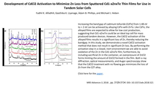
- 1. Development of CdCl2 Activation to Minimize Zn Loss from Sputtered Cd1-xZnxTe Thin Films for Use in Tandem Solar Cells Fadhil K. Alfadhili, Geethika K. Liyanage, Adam B. Phillips, and Michael J. Heben Increasing the band gap of cadmium telluride (CdTe) from 1.48 eV to > 2 eV can be achieved by alloying CdTe with ZnTe. Like CdTe, the alloyed films are expected to allow for low cost production, suggesting that Cd1-xZnxTe could be an ideal top cell for mass produced tandem devices. However, the CdCl2 activation of the alloyed films results in a significant loss of Zn, thereby reducing the bandgap. In this study, we demonstrate a novel CdCl2 activation method that does not result in significant Zn loss. By performing the activation step in a closed, inert environment we are able to avoid oxidation of the Zn in the Cd1-xZnxTe film; furthermore, by including sacrificial Zn in the container, an overpressure of ZnCl2 forms limiting the amount of ZnCl2 formed in the film. Both x-ray diffraction, optical measurements, and Auger spectroscopy show that the CdCl2 treatment with no flowing gas minimizes the loss of Zn from the CZT alloy. Click here for the paper. MRS Advances 3, 2018 , pp. 3129-3134. DOI: 10.1557/adv.2018.521 PL of CdCl2 of CdZnTe
- 2. Impact of Infrared Optical Properties on Crystalline Si and Thin Film CdTe Solar Cells Indra Subedi, Timothy J Silverman, Michael G. Deceglie, and Nikolas J. Podraza Photons with energies below the photovoltaic (PV) absorber band gap do not generate current and adversely impact performance when absorbed in other solar cell components to produce heat. Here we incorporate infrared (IR) optical response in simulations for understanding thermal losses. Spectroscopic ellipsometry is used to measure Al-Si interface optical properties in Si PV. Reflectance of an Si module has been analyzed to account for encapsulant and Al-Si interface contributions. IR extended quantum efficiency simulations calculate efficiency gains / losses arising from variations in current generated and total reflectance as functions of transparent front contact material in thin film CdTe PV. Click here for the paper. 44th IEEE Photovoltaic Specialists Conference (PVSC), Washington DC, 2017.
- 3. Glancing Angle Deposited CdTe: Optical Properties and Structure Dipendra Adhikari, Prakash Koirala, Maxwell M. Junda, Robert W. Collins, and Nikolas J. Podraza 7th World Conference on Photovoltaic Energy Conversion, Waikoloa, HI. 2018. Optical and microstructural properties of as-deposited CdTe films deposited on soda lime glass by magnetron sputtering at various source flux angles have been investigated using GIXRD, SEM, unpolarized transmittance / reflectance, and spectroscopic ellipsometry. Influence of deposition angle on resultant crystalline grain size and orientation are tracked for these films. All CdTe films studied are found to have cubic crystal structure and (111) preferential grain orientation. Films deposited at 0° and 45° are almost entirely (111) oriented, whereas films deposited at higher angles exhibit a wider variety of competing grain orientations, suggesting that deposition angle can be used as an effective parameter towards controlling grain orientation. With increasing numbers of grain orientations, grain size is found to decrease. Ex-situ spectroscopic ellipsometry is used to obtain the structural and optical properties. Stress induced in the film is calculated based on shifts of critical point energies. Click here for the paper.
- 4. Low Temperature Photoluminescence Spectroscopy of Defect and Interband Transitions in CdSexTe1-x Thin Films Niraj Shrestha, Corey R. Grice, Ebin Bastola, Geethika K. Liyanage, Adam B. Phillips, Michael J. Heben, Yanfa Yan, and Randy J. Ellingson We present the defect analysis by photoluminescence (PL) spectroscopy of CdSexTe1-x thin films, grown with varying Se content by a co-sputtered deposition method. We observe a peak at 1.203 eV in the CdSexTe1-x film for x = 0.21, which shifts towards higher energies with increase in laser power. This peak was assigned to a donor-to-acceptor (DAP) transition, with a measured j-shift of ~4.7 meV/decade. Temperature dependent PL intensity measurements confirm that the observed DAP peak involves a shallow defect state of binding energy ~34.7 meV. In contrast, a free-to-bound (FB) peak at 1.294 eV involving a shallow defect of binding energy ~18.3 meV was observed in the CdSexTe1-x film for x = 0.14. Additionally, we observe band edge emission at 1.452 eV and 1.448 eV in CdSexTe1-x films for x = 0.14 and x = 0.21 respectively. Our analysis shows that the Se concentration not only changes the band gap energy of the resulting CdSexTe1-x alloy thin film, but also modifies the nature of the dominant observed defect emission. Click here for the paper. MRS Advances 2018,1-7. doi: 10.1557/adv.2018.516 PL of CdSeTe
- 5. Development of CdCl2 Activation to Minimize Zn Loss from Sputtered Cd1-xZnxTe Thin Films for Use in Tandem Solar Cells Fadhil K. Alfadhili, Geethika K. Liyanage, Adam B. Phillips, and Michael J. Heben MRS Advances, 1-6 (2018); doi: 10.1557/adv.2018.521 We have developed a CdCl2 activation method that does not result in significant Zn loss for Cd1-xZnxTe thin films. By performing the activation step in a closed, inert environment we are able to avoid oxidation of the Zn in the Cd1-xZnxTe film; furthermore, by including sacrificial Zn in the container, an overpressure of ZnCl2 forms limiting the amount of ZnCl2 formed in the film. The results suggest that CdCl2 activation of Cd1-xZnxTe films in a static, inert atmosphere is well behaved and can be used for a controlled device processing. Click here for the paper.
- 6. Current Enhancement of CdTe-Based Solar Cells We report on the realization of CdTe solar cell photocurrent enhancement using an n-type CdSe heterojunction partner sputtered on commercial SnO2/SnO2:F coated soda-lime glass substrates. With high-temperature close-space sublimation CdTe deposition followed by CdCl2 activation, this thin-film stack allows for substantial interdiffusion at the CdSe/CdTe interface facilitating a CdSexTe1-x alloy formation. The bowing effect causes a reduced optical bandgap of the alloyed absorber layer and, therefore, leads to current enhancement in the long-wavelength region and a decrease in open-circuit voltage (VOC). To overcome the VOC loss and maintain a high short-circuit current (JSC), the CdTe cell configuration has been modified using combined CdS:O/CdSe window layers. The new device structure has demonstrated enhanced collection from both short-and long-wavelength regions as well as a VOC improvement. With an optimized synthesis process, a small-area cell using CdS:O/CdSe window layer showed an efficiency of 15.2% with a VOC of 831 mV, a JSC of 26.3 mA/cm2, and a fill factor of 69.5%, measured under an AM1.5 illumination without antireflection coating. The results provide new directions for further improvement of CdTe-based solar cells. Click here for the paper. Naba R. Paudel, Jonathan D. Poplawsky, Karren L. Moore, Yanfa Yan IEEE Journal of Photovoltaics, 5, 1492-1496 (2015); DOI: 10.1109/JPHOTOV.2015.2458040
- 7. High temperature CSS processed CdTe solar cells on commercial SnO2:F/SnO2 coated soda-lime glass substrates We report on the realization of CdS/CdTe solar cells grown on commercial SnO2:F/SnO2- coated soda-lime glass substrates with conversion efficiencies >16 % by careful optimization of fabrication processes, which consist of sequential deposition of magnetron sputtered CdS window layer and high temperature close-space sublimation of CdTe absorber, CdCl2 activation, and thermal evaporation of elemental Cu/Au bilayer back contacts. The optimization of CdS and CdTe depositions include the incorporation of small fraction of oxygen during the growth. In our fabrication, the optimal amount of O in the deposition ambient is 5 % for CdS deposition and 0.5 % for CdTe depositions. The incorporation of small amounts of O is found to enhance the short circuit current (JSC) and open circuit voltage (VOC) of CdTe solar cells. We further identified that the flow rate of the ambient gas during the CdS sputtering can also affect the performance of the CdTe solar cells. The optimal flow rate is 40 sccm for our fabrication process. With careful optimization of our synthesis steps, the best small-area cell has shown an efficiency of 16.4 % with a VOC of 858 mV, a JSC of 26.5 mA/cm2, and a fill-factor of 72.0 % measured under AM1.5G illumination. This cell was coated with a 100 nm thick magnesium fluoride anti-reflection coating layer on the glass side. Click here for the paper. Naba R. Paudel, Corey R. Grice, Chuanxiao Xiao, Yanfa Yan Journal of Materials Science: Materials in Electronics, 26, 4708-4715 (2015);DOI:10.1007/s10854-015-2923-5
- 8. Photoluminescence Spectroscopy of Cadmium Telluride Deep Defects Deep defect states of Cadmium Telluride deposited via close space sublimation and magnetron sputtering are evaluated via steady state and time resolved photoluminescence. Intensity dependent photoluminescence measurements for as-grown and cadmium chloride treated samples reveal the recombination mechanism associated with each transition. The as-grown sputtered film photoluminescence is weak with broad features while the close space sublimation film photoluminescence is comparatively bright and dominated by a deep donor acceptor pair recombination. Unlike excitonic or free-to-bound transitions, donor acceptor pair recombination exhibits a distance dependence that determines the distribution of transition energies and recombination rates. We measure the PL lifetime with respect to energy as a direct observation of the increasing donor acceptor pair recombination rate with decreasing donor-acceptor separation. Click here for the paper. Paul J. Roland, Naba R. Paudel, Chuanxiao Xiao, Yanfa Yan, Randy J. Ellingson 2014 IEEE 40th Photovoltaic Specialist Conference, Denver, CO, 2014. PL of CdTe Deep Defects