SlideShare a Scribd company logo
BF420, BF422

High Voltage Transistors
NPN Silicon
• Pb−Free Package is Available*
                                                                                                               http://onsemi.com
 MAXIMUM RATINGS
                 Rating                       Symbol      BF420        BF422       Unit                                COLLECTOR
                                                                                                                           2
  Collector −Emitter Voltage                       VCEO    300          250        Vdc
  Collector −Base Voltage                          VCBO    300          250        Vdc
                                                                                                                3
  Emitter −Base Voltage                            VEBO          5.0               Vdc                        BASE

  Collector Current − Continuous                    IC            50               mAdc
                                                                                                                          1
  Collector Current − Peak                         ICM           100               mA                                  EMITTER
  Total Device Dissipation (Note 1)                PD
    @ TA = 25°C                                                  830            mW
    Derate above 25°C                                            6.6           mW/°C
                                                                                                                                    MARKING
  Operating and Storage Junction               TJ, Tstg    −55 to +150              °C                                              DIAGRAM
   Temperature Range

 THERMAL CHARACTERISTICS
                                                                                                                                         BF
             Characteristic                   Symbol             Max               Unit                                                  42x
                                                                                                  1                                      AYWW
  Thermal Resistance,                              RqJA                            °C/W               2
                                                                                                          3
    Junction to Ambient                                          150
  Thermal Resistance,                              RqJL                            °C/W     TO−92 (TO−226AA)
    Junction to Lead                                              68                          CASE 29−11,
                                                                                               STYLE 14
Maximum ratings are those values beyond which device damage can occur.
Maximum ratings applied to the device are individual stress limit values (not
normal operating conditions) and are not valid simultaneously. If these limits are                            x    = 0 or 2
exceeded, device functional operation is not implied, damage may occur and                                    A    = Assembly Location
reliability may be affected.                                                                                  Y    = Year
1. Mounted on a FR4 board with 200 mm2 of 1 oz copper and lead length of                                      WW   = Work Week
    5 mm.

                                                                                                          ORDERING INFORMATION

                                                                                             Device                Package          Shipping†
                                                                                          BF420ZL1                  TO−92        2000 Ammo Pack
                                                                                          BF422                     TO−92         5000 Units/Box
                                                                                          BF422G                     TO−92        5000 Units/Box
                                                                                                                   (Pb−Free)
                                                                                          BF422RL1                  TO−92        2000 Tape & Reel
                                                                                          BF422ZL1                  TO−92        2000 Ammo Pack

                                                                                          †For information on tape and reel specifications,
                                                                                           including part orientation and tape sizes, please
                                                                                           refer to our Tape and Reel Packaging Specifications
                                                                                           Brochure, BRD8011/D.

*For additional information on our Pb−Free strategy and soldering details, please
 download the ON Semiconductor Soldering and Mounting Techniques
 Reference Manual, SOLDERRM/D.


© Semiconductor Components Industries, LLC, 2004                               1                                         Publication Order Number:
October, 2004 − Rev. 3                                                                                                                    BF420/D
BF420, BF422

ELECTRICAL CHARACTERISTICS (TA = 25°C unless otherwise noted)
                                    Characteristic                                Symbol     Min   Max    Unit

OFF CHARACTERISTICS
 Collector −Emitter Breakdown Voltage (Note 220                                   V(BR)CEO                Vdc
   (IC = 1.0 mAdc, IB = 0)                                                BF420              300   —
                                                                          BF422              250   —
 Collector −Base Breakdown Voltage                                                V(BR)CBO                Vdc
   (IC = 100 mAdc, IE = 0)                                                BF420              300   —
                                                                          BF422              250   —
 Emitter −Base Breakdown Voltage                                                  V(BR)EBO                Vdc
  (IE = 100 mAdc, IC = 0)                                                 BF420              5.0   —
                                                                          BF422              5.0   —
 Collector Cutoff Current                                                           ICBO                  µAdc
   (VCB = 200 Vdc, IE = 0)                                                BF420              —     0.01
                                                                          BF422              —      —
 Emitter Cutoff Current                                                             IEBO                  nAdc
  (VEB = 5.0 Vdc, IC = 0)                                                 BF420              —     100
                                                                          BF422              —      —

ON CHARACTERISTICS
 DC Current Gain                                                                    hFE                    —
  (IC = 25 mAdc, VCE = 20 Vdc)                                            BF420              50    —
                                                                          BF422              50    —
 Collector −Emitter Saturation Voltage                                            VCE(sat)                Vdc
   (IC = 20 mAdc, IB = 2.0 mAdc)                                                             —     0.5
 Base −Emitter Saturation Voltage                                                 VBE(sat)                Vdc
   (IC = 20 mAdc, IB = 2.0 mAdc)                                                             —     2.0

SMALL−SIGNAL CHARACTERISTICS
 Current Gain — Bandwidth Product                                                    fT                   MHz
   (IC = 10 mAdc, VCE = 10 Vdc, f = 20 MHz)                                                  60    —
 Common Emitter Feedback Capacitance                                                Cre                   pF
   (VCB = 30 Vdc, IE = 0, f = 1.0 MHz)                                                       —     1.6

2. Pulse Test: Pulse Width v 300 ms; Duty Cycle v 2.0%.


                                                      http://onsemi.com
                                                              2
BF420, BF422

                      120
                                                                                                                                                         VCE = 10 Vdc
                                                TJ = +125°C
                      100
   hFE , DC CURRENT GAIN


                           80

                                                  25°C
                           60

                           40
                                                  −55°C
                           20

                            0
                                 0.1                              1.0                                                      10                                            100
                                                                         IC, COLLECTOR CURRENT (mA)

                                                                        Figure 1. DC Current Gain


                      100                                                                                     80


                                                                                          BANDWIDTH (MHz)
                                                    Ceb @ 1MHz                                                70

                                                                                                              60
C, CAPACITANCE (pF)


                           10
                                                                                                              50
                                                                                          f T, CURRENT−GAIN


                                                                                                              40
                           1.0               Ccb @ 1MHz
                                                                                                              30                                              TJ = 25°C
                                                                                                                                                              VCE = 20 V
                                                                                                              20                                              f = 20 MHz

                           0.1                                                                                10
                              0.1      1.0            10          100          1000                             1.0   2.0 3.0       5.0 7.0 10     20   30        50 70 100
                                         VR, REVERSE VOLTAGE (VOLTS)                                                            IC, COLLECTOR CURRENT (mA)

                                         Figure 2. Capacitance                                                        Figure 3. Current−Gain − Bandwidth


                            1.4

                            1.2
                                                                                                                                               VCE(sat) @ 25°C, IC/IB = 10
                                                                                                                                               VCE(sat) @ 125°C, IC/IB = 10
 V, VOLTAGE (VOLTS)


                            1.0
                                                                                                                                               VCE(sat) @ −55°C, IC/IB = 10
                            0.8                                                                                                                VBE(sat) @ 25°C, IC/IB = 10
                                                                                                                                               VBE(sat) @ 125°C, IC/IB = 10
                            0.6                                                                                                                VBE(sat) @ −55°C, IC/IB = 10
                                                                                                                                               VBE(on) @ 25°C, VCE = 10 V
                            0.4                                                                                                                VBE(on) @ 125°C, VCE = 10 V
                                                                                                                                               VBE(on) @ −55°C, VCE = 10 V
                            0.2

                            0.0
                               0.1            1.0             10                100
                                          IC, COLLECTOR CURRENT (mA)

                                         Figure 4. ”ON” Voltages


                                                                           http://onsemi.com
                                                                                      3
BF420, BF422

                                                                          PACKAGE DIMENSIONS

                                                                                  TO−92 (TO−226)
                                                                                   CASE 029−11
                                                                                    ISSUE AJ


                                                                                                                                       NOTES:
                                                                                                                                        1. DIMENSIONING AND TOLERANCING PER ANSI
                                             A                       B                                                                     Y14.5M, 1982.
                                                                                                                                        2. CONTROLLING DIMENSION: INCH.
                                                                                                                                        3. CONTOUR OF PACKAGE BEYOND DIMENSION R
                                                                                                                                           IS UNCONTROLLED.
                              R                                                                                                         4. LEAD DIMENSION IS UNCONTROLLED IN P AND
                                                                                                                                           BEYOND DIMENSION K MINIMUM.
                                                         P
                                                             L                                                                                         INCHES       MILLIMETERS
                      SEATING                                                                                                                DIM    MIN     MAX      MIN   MAX
                      PLANE                                      K                                                                            A    0.175   0.205     4.45   5.20
                                                                                                                                              B    0.170   0.210     4.32   5.33
                                                                                                                                              C    0.125   0.165     3.18   4.19
                                                                                                                                              D    0.016   0.021    0.407  0.533
                                                                                                                                              G    0.045   0.055     1.15   1.39
                                     X X                                                  D                                                   H    0.095   0.105     2.42   2.66
                                                     G                                                                                        J    0.015   0.020     0.39   0.50
                                                                                                                                              K    0.500     −−−    12.70    −−−
                                             H                                                     J                                          L    0.250     −−−     6.35    −−−
                                                                                                                                              N    0.080   0.105     2.04   2.66
                                             V                C                                                                               P      −−−   0.100      −−−   2.54
                                                                                                                                              R    0.115     −−−     2.93    −−−
                                                                                  SECTION X−X                                                 V    0.135     −−−     3.43    −−−
                                         1               N
                                                 N
                                                                                                                                               STYLE 14:
                                                                                                                                                 PIN 1. EMITTER
                                                                                                                                                     2. COLLECTOR
                                                                                                                                                     3. BASE


 ON Semiconductor and             are registered trademarks of Semiconductor Components Industries, LLC (SCILLC). SCILLC reserves the right to make changes without further notice
 to any products herein. SCILLC makes no warranty, representation or guarantee regarding the suitability of its products for any particular purpose, nor does SCILLC assume any liability
 arising out of the application or use of any product or circuit, and specifically disclaims any and all liability, including without limitation special, consequential or incidental damages.
 “Typical” parameters which may be provided in SCILLC data sheets and/or specifications can and do vary in different applications and actual performance may vary over time. All
 operating parameters, including “Typicals” must be validated for each customer application by customer’s technical experts. SCILLC does not convey any license under its patent rights
 nor the rights of others. SCILLC products are not designed, intended, or authorized for use as components in systems intended for surgical implant into the body, or other applications
 intended to support or sustain life, or for any other application in which the failure of the SCILLC product could create a situation where personal injury or death may occur. Should
 Buyer purchase or use SCILLC products for any such unintended or unauthorized application, Buyer shall indemnify and hold SCILLC and its officers, employees, subsidiaries, affiliates,
 and distributors harmless against all claims, costs, damages, and expenses, and reasonable attorney fees arising out of, directly or indirectly, any claim of personal injury or death
 associated with such unintended or unauthorized use, even if such claim alleges that SCILLC was negligent regarding the design or manufacture of the part. SCILLC is an Equal
 Opportunity/Affirmative Action Employer. This literature is subject to all applicable copyright laws and is not for resale in any manner.


PUBLICATION ORDERING INFORMATION
LITERATURE FULFILLMENT:                                                  N. American Technical Support: 800−282−9855 Toll Free             ON Semiconductor Website: http://onsemi.com
 Literature Distribution Center for ON Semiconductor                     USA/Canada
 P.O. Box 61312, Phoenix, Arizona 85082−1312 USA                                                                                           Order Literature: http://www.onsemi.com/litorder
 Phone: 480−829−7710 or 800−344−3860 Toll Free USA/Canada                Japan: ON Semiconductor, Japan Customer Focus Center
 Fax: 480−829−7709 or 800−344−3867 Toll Free USA/Canada                   2−9−1 Kamimeguro, Meguro−ku, Tokyo, Japan 153−0051               For additional information, please contact your
 Email: orderlit@onsemi.com                                               Phone: 81−3−5773−3850                                            local Sales Representative.


                                                                                http://onsemi.com                                                                                BF420/D
                                                                                              4
This datasheet has been download from:

      www.datasheetcatalog.com

Datasheets for electronics components.

More Related Content

What's hot

4057
40574057
www.eclipselightinginc.com
www.eclipselightinginc.comwww.eclipselightinginc.com
Mc 33078n op amp dual lo noise
Mc 33078n op amp dual lo noiseMc 33078n op amp dual lo noise
Mc 33078n op amp dual lo noise
vakumtube
 
Si1029X
Si1029XSi1029X
Si1029X
spicepark
 
G.r.s. 02 04-01-12
G.r.s. 02 04-01-12G.r.s. 02 04-01-12
G.r.s. 02 04-01-12
angeloneha
 
Bdiscom flyer en_07
Bdiscom flyer en_07Bdiscom flyer en_07
Bdiscom flyer en_07
bdiscom
 
LM324 Low Power Quad Op Amps
LM324 Low Power Quad Op AmpsLM324 Low Power Quad Op Amps
LM324 Low Power Quad Op Amps
Yong Heui Cho
 
Mean well rs-25
Mean well   rs-25Mean well   rs-25
Mean well rs-25
Advantec Distribution
 
2 page s40 data sheet
2 page s40 data sheet2 page s40 data sheet
2 page s40 data sheet
Mas'Angga Kusuma
 
WEBINAR - VIPer Plus
WEBINAR - VIPer PlusWEBINAR - VIPer Plus
WEBINAR - VIPer Plus
STMicroelectronics
 
Cmos scaling on resistive component 2012
Cmos scaling on resistive component 2012Cmos scaling on resistive component 2012
Cmos scaling on resistive component 2012
Sidewinder2011
 
Nfpa scan pgs 30 34
Nfpa scan pgs 30 34Nfpa scan pgs 30 34
Nfpa scan pgs 30 34
guestf8e1f7
 
A DC-6 GHz, Packaged 100 Watt GaN SPDT Switch MMIC
A DC-6 GHz, Packaged 100 Watt GaN SPDT Switch MMICA DC-6 GHz, Packaged 100 Watt GaN SPDT Switch MMIC
A DC-6 GHz, Packaged 100 Watt GaN SPDT Switch MMIC
Sushil Kumar
 
Vip Er22a
Vip Er22aVip Er22a
Vip Er22a
guest1ce360f
 
DVD Player Multiple Output Di115 2
DVD Player Multiple Output Di115 2DVD Player Multiple Output Di115 2
DVD Player Multiple Output Di115 2
gueste54184
 
1k
1k1k
9730 datasheet
9730 datasheet9730 datasheet
9730 datasheet
Quantum Composers
 
Mean well net-75 triple out
Mean well   net-75 triple outMean well   net-75 triple out
Mean well net-75 triple out
Advantec Distribution
 
Ctc177 Aa3 Chassis Tv Rca
Ctc177 Aa3 Chassis Tv RcaCtc177 Aa3 Chassis Tv Rca
Ctc177 Aa3 Chassis Tv Rca
guestc30a06
 

What's hot (19)

4057
40574057
4057
 
www.eclipselightinginc.com
www.eclipselightinginc.comwww.eclipselightinginc.com
www.eclipselightinginc.com
 
Mc 33078n op amp dual lo noise
Mc 33078n op amp dual lo noiseMc 33078n op amp dual lo noise
Mc 33078n op amp dual lo noise
 
Si1029X
Si1029XSi1029X
Si1029X
 
G.r.s. 02 04-01-12
G.r.s. 02 04-01-12G.r.s. 02 04-01-12
G.r.s. 02 04-01-12
 
Bdiscom flyer en_07
Bdiscom flyer en_07Bdiscom flyer en_07
Bdiscom flyer en_07
 
LM324 Low Power Quad Op Amps
LM324 Low Power Quad Op AmpsLM324 Low Power Quad Op Amps
LM324 Low Power Quad Op Amps
 
Mean well rs-25
Mean well   rs-25Mean well   rs-25
Mean well rs-25
 
2 page s40 data sheet
2 page s40 data sheet2 page s40 data sheet
2 page s40 data sheet
 
WEBINAR - VIPer Plus
WEBINAR - VIPer PlusWEBINAR - VIPer Plus
WEBINAR - VIPer Plus
 
Cmos scaling on resistive component 2012
Cmos scaling on resistive component 2012Cmos scaling on resistive component 2012
Cmos scaling on resistive component 2012
 
Nfpa scan pgs 30 34
Nfpa scan pgs 30 34Nfpa scan pgs 30 34
Nfpa scan pgs 30 34
 
A DC-6 GHz, Packaged 100 Watt GaN SPDT Switch MMIC
A DC-6 GHz, Packaged 100 Watt GaN SPDT Switch MMICA DC-6 GHz, Packaged 100 Watt GaN SPDT Switch MMIC
A DC-6 GHz, Packaged 100 Watt GaN SPDT Switch MMIC
 
Vip Er22a
Vip Er22aVip Er22a
Vip Er22a
 
DVD Player Multiple Output Di115 2
DVD Player Multiple Output Di115 2DVD Player Multiple Output Di115 2
DVD Player Multiple Output Di115 2
 
1k
1k1k
1k
 
9730 datasheet
9730 datasheet9730 datasheet
9730 datasheet
 
Mean well net-75 triple out
Mean well   net-75 triple outMean well   net-75 triple out
Mean well net-75 triple out
 
Ctc177 Aa3 Chassis Tv Rca
Ctc177 Aa3 Chassis Tv RcaCtc177 Aa3 Chassis Tv Rca
Ctc177 Aa3 Chassis Tv Rca
 

Viewers also liked

Fredi satya acrs
Fredi satya acrsFredi satya acrs
Fredi satya acrs
Fredi Rosaji
 
Asma_Altaf_wiki_activate_week#2
Asma_Altaf_wiki_activate_week#2Asma_Altaf_wiki_activate_week#2
Asma_Altaf_wiki_activate_week#2
asmaaltaf
 
What is GLASS
What is GLASSWhat is GLASS
What is GLASS
RLI-Mike
 
Edvīns Karnītis: Vienotais universālā pakalpojuma modelis Latvijā; elektroene...
Edvīns Karnītis: Vienotais universālā pakalpojuma modelis Latvijā; elektroene...Edvīns Karnītis: Vienotais universālā pakalpojuma modelis Latvijā; elektroene...
Edvīns Karnītis: Vienotais universālā pakalpojuma modelis Latvijā; elektroene...eu_skarbi
 
Asma Altaf wiki_activate_Week#2
Asma Altaf wiki_activate_Week#2Asma Altaf wiki_activate_Week#2
Asma Altaf wiki_activate_Week#2
asmaaltaf
 
Falar verdade a mentir
Falar verdade a mentirFalar verdade a mentir
Falar verdade a mentir
PDPBDelgado
 
RLI RLF collaboration
RLI RLF collaborationRLI RLF collaboration
RLI RLF collaboration
RLI-Mike
 
Syndication offering for NHS organisations
Syndication offering for NHS organisationsSyndication offering for NHS organisations
Syndication offering for NHS organisations
seashaped
 
El poder del creador de Software. Entre la ingeniería y la artesanía
El poder del creador de Software. Entre la ingeniería y la artesaníaEl poder del creador de Software. Entre la ingeniería y la artesanía
El poder del creador de Software. Entre la ingeniería y la artesanía
David Gómez García
 

Viewers also liked (10)

Kalai2
Kalai2Kalai2
Kalai2
 
Fredi satya acrs
Fredi satya acrsFredi satya acrs
Fredi satya acrs
 
Asma_Altaf_wiki_activate_week#2
Asma_Altaf_wiki_activate_week#2Asma_Altaf_wiki_activate_week#2
Asma_Altaf_wiki_activate_week#2
 
What is GLASS
What is GLASSWhat is GLASS
What is GLASS
 
Edvīns Karnītis: Vienotais universālā pakalpojuma modelis Latvijā; elektroene...
Edvīns Karnītis: Vienotais universālā pakalpojuma modelis Latvijā; elektroene...Edvīns Karnītis: Vienotais universālā pakalpojuma modelis Latvijā; elektroene...
Edvīns Karnītis: Vienotais universālā pakalpojuma modelis Latvijā; elektroene...
 
Asma Altaf wiki_activate_Week#2
Asma Altaf wiki_activate_Week#2Asma Altaf wiki_activate_Week#2
Asma Altaf wiki_activate_Week#2
 
Falar verdade a mentir
Falar verdade a mentirFalar verdade a mentir
Falar verdade a mentir
 
RLI RLF collaboration
RLI RLF collaborationRLI RLF collaboration
RLI RLF collaboration
 
Syndication offering for NHS organisations
Syndication offering for NHS organisationsSyndication offering for NHS organisations
Syndication offering for NHS organisations
 
El poder del creador de Software. Entre la ingeniería y la artesanía
El poder del creador de Software. Entre la ingeniería y la artesaníaEl poder del creador de Software. Entre la ingeniería y la artesanía
El poder del creador de Software. Entre la ingeniería y la artesanía
 

Similar to Bf422

2 n60
2 n602 n60
Mur880 dioso simple
Mur880 dioso simpleMur880 dioso simple
Mur880 dioso simple
Kenyu Luque Huaman
 
Ka431
Ka431Ka431
Ka431
rafanate20
 
Maitry Instruments & Control, Surat, Process Control Instruments
Maitry Instruments & Control, Surat, Process Control InstrumentsMaitry Instruments & Control, Surat, Process Control Instruments
Maitry Instruments & Control, Surat, Process Control Instruments
IndiaMART InterMESH Limited
 
Sfp(ft 9001 g-m-lc02)-datasheet_ver_1.1
Sfp(ft 9001 g-m-lc02)-datasheet_ver_1.1Sfp(ft 9001 g-m-lc02)-datasheet_ver_1.1
Sfp(ft 9001 g-m-lc02)-datasheet_ver_1.1
Feliz Technology Co., Ltd.
 
Power amplifier (1)
Power amplifier (1) Power amplifier (1)
Power amplifier (1)
Nadhiien Abraham
 
Ppt 2
Ppt 2Ppt 2
Ppt 2
JM_IEEE
 
DS25CP102 (English)
DS25CP102 (English)DS25CP102 (English)
DS25CP102 (English)
Tsuyoshi Horigome
 
Lm 337 datasheet
Lm 337 datasheetLm 337 datasheet
Lm 337 datasheet
Andy Medina
 
Lm741
Lm741Lm741
Lm741
vivi678
 
Htr india-products-wire-wound-resistors-silicone-coated-resistors-hfw-english
Htr india-products-wire-wound-resistors-silicone-coated-resistors-hfw-englishHtr india-products-wire-wound-resistors-silicone-coated-resistors-hfw-english
Htr india-products-wire-wound-resistors-silicone-coated-resistors-hfw-english
htrindia
 
HFW - FUSIBLE RESISTORS SILICONE / CEMENT COATED
HFW - FUSIBLE RESISTORS SILICONE / CEMENT COATEDHFW - FUSIBLE RESISTORS SILICONE / CEMENT COATED
HFW - FUSIBLE RESISTORS SILICONE / CEMENT COATED
htrindia
 
Original N-Channel Mosfet UTC7N65L-TF1-T 7N65 7.4A 650V TO-220F New Techcod
Original N-Channel Mosfet UTC7N65L-TF1-T 7N65 7.4A 650V TO-220F New TechcodOriginal N-Channel Mosfet UTC7N65L-TF1-T 7N65 7.4A 650V TO-220F New Techcod
Original N-Channel Mosfet UTC7N65L-TF1-T 7N65 7.4A 650V TO-220F New Techcod
AUTHELECTRONIC
 
SFP(FT-901B-S-LC20)_DataSheet_ver_1.1
SFP(FT-901B-S-LC20)_DataSheet_ver_1.1SFP(FT-901B-S-LC20)_DataSheet_ver_1.1
SFP(FT-901B-S-LC20)_DataSheet_ver_1.1
Feliz Technology Co., Ltd.
 
Sfp(ft 901 b-s-lc20)-datasheet_ver_1.1
Sfp(ft 901 b-s-lc20)-datasheet_ver_1.1Sfp(ft 901 b-s-lc20)-datasheet_ver_1.1
Sfp(ft 901 b-s-lc20)-datasheet_ver_1.1
Feliz Technology Co., Ltd.
 
Htr india-products-wire-wound-resistors-silicone-coated-resistors-hfw-english...
Htr india-products-wire-wound-resistors-silicone-coated-resistors-hfw-english...Htr india-products-wire-wound-resistors-silicone-coated-resistors-hfw-english...
Htr india-products-wire-wound-resistors-silicone-coated-resistors-hfw-english...
htrindia
 
Htr india-products-wire-wound-resistors-silicone-coated-resistors-hfw-english
Htr india-products-wire-wound-resistors-silicone-coated-resistors-hfw-englishHtr india-products-wire-wound-resistors-silicone-coated-resistors-hfw-english
Htr india-products-wire-wound-resistors-silicone-coated-resistors-hfw-english
SiddheshPathak3
 
Htr india-products-wire-wound-resistors-silicone-coated-resistors-hfw-english
Htr india-products-wire-wound-resistors-silicone-coated-resistors-hfw-englishHtr india-products-wire-wound-resistors-silicone-coated-resistors-hfw-english
Htr india-products-wire-wound-resistors-silicone-coated-resistors-hfw-english
htrindia
 
SFP(FT-901B-S-LC20)_DataSheet_ver_1_2
SFP(FT-901B-S-LC20)_DataSheet_ver_1_2SFP(FT-901B-S-LC20)_DataSheet_ver_1_2
SFP(FT-901B-S-LC20)_DataSheet_ver_1_2
Feliz Technology Co., Ltd.
 
By329 diodo simple
By329 diodo simpleBy329 diodo simple
By329 diodo simple
Kenyu Luque Huaman
 

Similar to Bf422 (20)

2 n60
2 n602 n60
2 n60
 
Mur880 dioso simple
Mur880 dioso simpleMur880 dioso simple
Mur880 dioso simple
 
Ka431
Ka431Ka431
Ka431
 
Maitry Instruments & Control, Surat, Process Control Instruments
Maitry Instruments & Control, Surat, Process Control InstrumentsMaitry Instruments & Control, Surat, Process Control Instruments
Maitry Instruments & Control, Surat, Process Control Instruments
 
Sfp(ft 9001 g-m-lc02)-datasheet_ver_1.1
Sfp(ft 9001 g-m-lc02)-datasheet_ver_1.1Sfp(ft 9001 g-m-lc02)-datasheet_ver_1.1
Sfp(ft 9001 g-m-lc02)-datasheet_ver_1.1
 
Power amplifier (1)
Power amplifier (1) Power amplifier (1)
Power amplifier (1)
 
Ppt 2
Ppt 2Ppt 2
Ppt 2
 
DS25CP102 (English)
DS25CP102 (English)DS25CP102 (English)
DS25CP102 (English)
 
Lm 337 datasheet
Lm 337 datasheetLm 337 datasheet
Lm 337 datasheet
 
Lm741
Lm741Lm741
Lm741
 
Htr india-products-wire-wound-resistors-silicone-coated-resistors-hfw-english
Htr india-products-wire-wound-resistors-silicone-coated-resistors-hfw-englishHtr india-products-wire-wound-resistors-silicone-coated-resistors-hfw-english
Htr india-products-wire-wound-resistors-silicone-coated-resistors-hfw-english
 
HFW - FUSIBLE RESISTORS SILICONE / CEMENT COATED
HFW - FUSIBLE RESISTORS SILICONE / CEMENT COATEDHFW - FUSIBLE RESISTORS SILICONE / CEMENT COATED
HFW - FUSIBLE RESISTORS SILICONE / CEMENT COATED
 
Original N-Channel Mosfet UTC7N65L-TF1-T 7N65 7.4A 650V TO-220F New Techcod
Original N-Channel Mosfet UTC7N65L-TF1-T 7N65 7.4A 650V TO-220F New TechcodOriginal N-Channel Mosfet UTC7N65L-TF1-T 7N65 7.4A 650V TO-220F New Techcod
Original N-Channel Mosfet UTC7N65L-TF1-T 7N65 7.4A 650V TO-220F New Techcod
 
SFP(FT-901B-S-LC20)_DataSheet_ver_1.1
SFP(FT-901B-S-LC20)_DataSheet_ver_1.1SFP(FT-901B-S-LC20)_DataSheet_ver_1.1
SFP(FT-901B-S-LC20)_DataSheet_ver_1.1
 
Sfp(ft 901 b-s-lc20)-datasheet_ver_1.1
Sfp(ft 901 b-s-lc20)-datasheet_ver_1.1Sfp(ft 901 b-s-lc20)-datasheet_ver_1.1
Sfp(ft 901 b-s-lc20)-datasheet_ver_1.1
 
Htr india-products-wire-wound-resistors-silicone-coated-resistors-hfw-english...
Htr india-products-wire-wound-resistors-silicone-coated-resistors-hfw-english...Htr india-products-wire-wound-resistors-silicone-coated-resistors-hfw-english...
Htr india-products-wire-wound-resistors-silicone-coated-resistors-hfw-english...
 
Htr india-products-wire-wound-resistors-silicone-coated-resistors-hfw-english
Htr india-products-wire-wound-resistors-silicone-coated-resistors-hfw-englishHtr india-products-wire-wound-resistors-silicone-coated-resistors-hfw-english
Htr india-products-wire-wound-resistors-silicone-coated-resistors-hfw-english
 
Htr india-products-wire-wound-resistors-silicone-coated-resistors-hfw-english
Htr india-products-wire-wound-resistors-silicone-coated-resistors-hfw-englishHtr india-products-wire-wound-resistors-silicone-coated-resistors-hfw-english
Htr india-products-wire-wound-resistors-silicone-coated-resistors-hfw-english
 
SFP(FT-901B-S-LC20)_DataSheet_ver_1_2
SFP(FT-901B-S-LC20)_DataSheet_ver_1_2SFP(FT-901B-S-LC20)_DataSheet_ver_1_2
SFP(FT-901B-S-LC20)_DataSheet_ver_1_2
 
By329 diodo simple
By329 diodo simpleBy329 diodo simple
By329 diodo simple
 

Recently uploaded

SWOT analysis in the project Keeping the Memory @live.pptx
SWOT analysis in the project Keeping the Memory @live.pptxSWOT analysis in the project Keeping the Memory @live.pptx
SWOT analysis in the project Keeping the Memory @live.pptx
zuzanka
 
Présentationvvvvvvvvvvvvvvvvvvvvvvvvvvvv2.pptx
Présentationvvvvvvvvvvvvvvvvvvvvvvvvvvvv2.pptxPrésentationvvvvvvvvvvvvvvvvvvvvvvvvvvvv2.pptx
Présentationvvvvvvvvvvvvvvvvvvvvvvvvvvvv2.pptx
siemaillard
 
UGC NET Exam Paper 1- Unit 1:Teaching Aptitude
UGC NET Exam Paper 1- Unit 1:Teaching AptitudeUGC NET Exam Paper 1- Unit 1:Teaching Aptitude
UGC NET Exam Paper 1- Unit 1:Teaching Aptitude
S. Raj Kumar
 
B. Ed Syllabus for babasaheb ambedkar education university.pdf
B. Ed Syllabus for babasaheb ambedkar education university.pdfB. Ed Syllabus for babasaheb ambedkar education university.pdf
B. Ed Syllabus for babasaheb ambedkar education university.pdf
BoudhayanBhattachari
 
Temple of Asclepius in Thrace. Excavation results
Temple of Asclepius in Thrace. Excavation resultsTemple of Asclepius in Thrace. Excavation results
Temple of Asclepius in Thrace. Excavation results
Krassimira Luka
 
Stack Memory Organization of 8086 Microprocessor
Stack Memory Organization of 8086 MicroprocessorStack Memory Organization of 8086 Microprocessor
Stack Memory Organization of 8086 Microprocessor
JomonJoseph58
 
Jemison, MacLaughlin, and Majumder "Broadening Pathways for Editors and Authors"
Jemison, MacLaughlin, and Majumder "Broadening Pathways for Editors and Authors"Jemison, MacLaughlin, and Majumder "Broadening Pathways for Editors and Authors"
Jemison, MacLaughlin, and Majumder "Broadening Pathways for Editors and Authors"
National Information Standards Organization (NISO)
 
Philippine Edukasyong Pantahanan at Pangkabuhayan (EPP) Curriculum
Philippine Edukasyong Pantahanan at Pangkabuhayan (EPP) CurriculumPhilippine Edukasyong Pantahanan at Pangkabuhayan (EPP) Curriculum
Philippine Edukasyong Pantahanan at Pangkabuhayan (EPP) Curriculum
MJDuyan
 
Leveraging Generative AI to Drive Nonprofit Innovation
Leveraging Generative AI to Drive Nonprofit InnovationLeveraging Generative AI to Drive Nonprofit Innovation
Leveraging Generative AI to Drive Nonprofit Innovation
TechSoup
 
Walmart Business+ and Spark Good for Nonprofits.pdf
Walmart Business+ and Spark Good for Nonprofits.pdfWalmart Business+ and Spark Good for Nonprofits.pdf
Walmart Business+ and Spark Good for Nonprofits.pdf
TechSoup
 
Traditional Musical Instruments of Arunachal Pradesh and Uttar Pradesh - RAYH...
Traditional Musical Instruments of Arunachal Pradesh and Uttar Pradesh - RAYH...Traditional Musical Instruments of Arunachal Pradesh and Uttar Pradesh - RAYH...
Traditional Musical Instruments of Arunachal Pradesh and Uttar Pradesh - RAYH...
imrankhan141184
 
BÀI TẬP DẠY THÊM TIẾNG ANH LỚP 7 CẢ NĂM FRIENDS PLUS SÁCH CHÂN TRỜI SÁNG TẠO ...
BÀI TẬP DẠY THÊM TIẾNG ANH LỚP 7 CẢ NĂM FRIENDS PLUS SÁCH CHÂN TRỜI SÁNG TẠO ...BÀI TẬP DẠY THÊM TIẾNG ANH LỚP 7 CẢ NĂM FRIENDS PLUS SÁCH CHÂN TRỜI SÁNG TẠO ...
BÀI TẬP DẠY THÊM TIẾNG ANH LỚP 7 CẢ NĂM FRIENDS PLUS SÁCH CHÂN TRỜI SÁNG TẠO ...
Nguyen Thanh Tu Collection
 
BÀI TẬP BỔ TRỢ TIẾNG ANH 8 CẢ NĂM - GLOBAL SUCCESS - NĂM HỌC 2023-2024 (CÓ FI...
BÀI TẬP BỔ TRỢ TIẾNG ANH 8 CẢ NĂM - GLOBAL SUCCESS - NĂM HỌC 2023-2024 (CÓ FI...BÀI TẬP BỔ TRỢ TIẾNG ANH 8 CẢ NĂM - GLOBAL SUCCESS - NĂM HỌC 2023-2024 (CÓ FI...
BÀI TẬP BỔ TRỢ TIẾNG ANH 8 CẢ NĂM - GLOBAL SUCCESS - NĂM HỌC 2023-2024 (CÓ FI...
Nguyen Thanh Tu Collection
 
A Visual Guide to 1 Samuel | A Tale of Two Hearts
A Visual Guide to 1 Samuel | A Tale of Two HeartsA Visual Guide to 1 Samuel | A Tale of Two Hearts
A Visual Guide to 1 Samuel | A Tale of Two Hearts
Steve Thomason
 
The History of Stoke Newington Street Names
The History of Stoke Newington Street NamesThe History of Stoke Newington Street Names
The History of Stoke Newington Street Names
History of Stoke Newington
 
RESULTS OF THE EVALUATION QUESTIONNAIRE.pptx
RESULTS OF THE EVALUATION QUESTIONNAIRE.pptxRESULTS OF THE EVALUATION QUESTIONNAIRE.pptx
RESULTS OF THE EVALUATION QUESTIONNAIRE.pptx
zuzanka
 
RHEOLOGY Physical pharmaceutics-II notes for B.pharm 4th sem students
RHEOLOGY Physical pharmaceutics-II notes for B.pharm 4th sem studentsRHEOLOGY Physical pharmaceutics-II notes for B.pharm 4th sem students
RHEOLOGY Physical pharmaceutics-II notes for B.pharm 4th sem students
Himanshu Rai
 
math operations ued in python and all used
math operations ued in python and all usedmath operations ued in python and all used
math operations ued in python and all used
ssuser13ffe4
 
How to Make a Field Mandatory in Odoo 17
How to Make a Field Mandatory in Odoo 17How to Make a Field Mandatory in Odoo 17
How to Make a Field Mandatory in Odoo 17
Celine George
 
LAND USE LAND COVER AND NDVI OF MIRZAPUR DISTRICT, UP
LAND USE LAND COVER AND NDVI OF MIRZAPUR DISTRICT, UPLAND USE LAND COVER AND NDVI OF MIRZAPUR DISTRICT, UP
LAND USE LAND COVER AND NDVI OF MIRZAPUR DISTRICT, UP
RAHUL
 

Recently uploaded (20)

SWOT analysis in the project Keeping the Memory @live.pptx
SWOT analysis in the project Keeping the Memory @live.pptxSWOT analysis in the project Keeping the Memory @live.pptx
SWOT analysis in the project Keeping the Memory @live.pptx
 
Présentationvvvvvvvvvvvvvvvvvvvvvvvvvvvv2.pptx
Présentationvvvvvvvvvvvvvvvvvvvvvvvvvvvv2.pptxPrésentationvvvvvvvvvvvvvvvvvvvvvvvvvvvv2.pptx
Présentationvvvvvvvvvvvvvvvvvvvvvvvvvvvv2.pptx
 
UGC NET Exam Paper 1- Unit 1:Teaching Aptitude
UGC NET Exam Paper 1- Unit 1:Teaching AptitudeUGC NET Exam Paper 1- Unit 1:Teaching Aptitude
UGC NET Exam Paper 1- Unit 1:Teaching Aptitude
 
B. Ed Syllabus for babasaheb ambedkar education university.pdf
B. Ed Syllabus for babasaheb ambedkar education university.pdfB. Ed Syllabus for babasaheb ambedkar education university.pdf
B. Ed Syllabus for babasaheb ambedkar education university.pdf
 
Temple of Asclepius in Thrace. Excavation results
Temple of Asclepius in Thrace. Excavation resultsTemple of Asclepius in Thrace. Excavation results
Temple of Asclepius in Thrace. Excavation results
 
Stack Memory Organization of 8086 Microprocessor
Stack Memory Organization of 8086 MicroprocessorStack Memory Organization of 8086 Microprocessor
Stack Memory Organization of 8086 Microprocessor
 
Jemison, MacLaughlin, and Majumder "Broadening Pathways for Editors and Authors"
Jemison, MacLaughlin, and Majumder "Broadening Pathways for Editors and Authors"Jemison, MacLaughlin, and Majumder "Broadening Pathways for Editors and Authors"
Jemison, MacLaughlin, and Majumder "Broadening Pathways for Editors and Authors"
 
Philippine Edukasyong Pantahanan at Pangkabuhayan (EPP) Curriculum
Philippine Edukasyong Pantahanan at Pangkabuhayan (EPP) CurriculumPhilippine Edukasyong Pantahanan at Pangkabuhayan (EPP) Curriculum
Philippine Edukasyong Pantahanan at Pangkabuhayan (EPP) Curriculum
 
Leveraging Generative AI to Drive Nonprofit Innovation
Leveraging Generative AI to Drive Nonprofit InnovationLeveraging Generative AI to Drive Nonprofit Innovation
Leveraging Generative AI to Drive Nonprofit Innovation
 
Walmart Business+ and Spark Good for Nonprofits.pdf
Walmart Business+ and Spark Good for Nonprofits.pdfWalmart Business+ and Spark Good for Nonprofits.pdf
Walmart Business+ and Spark Good for Nonprofits.pdf
 
Traditional Musical Instruments of Arunachal Pradesh and Uttar Pradesh - RAYH...
Traditional Musical Instruments of Arunachal Pradesh and Uttar Pradesh - RAYH...Traditional Musical Instruments of Arunachal Pradesh and Uttar Pradesh - RAYH...
Traditional Musical Instruments of Arunachal Pradesh and Uttar Pradesh - RAYH...
 
BÀI TẬP DẠY THÊM TIẾNG ANH LỚP 7 CẢ NĂM FRIENDS PLUS SÁCH CHÂN TRỜI SÁNG TẠO ...
BÀI TẬP DẠY THÊM TIẾNG ANH LỚP 7 CẢ NĂM FRIENDS PLUS SÁCH CHÂN TRỜI SÁNG TẠO ...BÀI TẬP DẠY THÊM TIẾNG ANH LỚP 7 CẢ NĂM FRIENDS PLUS SÁCH CHÂN TRỜI SÁNG TẠO ...
BÀI TẬP DẠY THÊM TIẾNG ANH LỚP 7 CẢ NĂM FRIENDS PLUS SÁCH CHÂN TRỜI SÁNG TẠO ...
 
BÀI TẬP BỔ TRỢ TIẾNG ANH 8 CẢ NĂM - GLOBAL SUCCESS - NĂM HỌC 2023-2024 (CÓ FI...
BÀI TẬP BỔ TRỢ TIẾNG ANH 8 CẢ NĂM - GLOBAL SUCCESS - NĂM HỌC 2023-2024 (CÓ FI...BÀI TẬP BỔ TRỢ TIẾNG ANH 8 CẢ NĂM - GLOBAL SUCCESS - NĂM HỌC 2023-2024 (CÓ FI...
BÀI TẬP BỔ TRỢ TIẾNG ANH 8 CẢ NĂM - GLOBAL SUCCESS - NĂM HỌC 2023-2024 (CÓ FI...
 
A Visual Guide to 1 Samuel | A Tale of Two Hearts
A Visual Guide to 1 Samuel | A Tale of Two HeartsA Visual Guide to 1 Samuel | A Tale of Two Hearts
A Visual Guide to 1 Samuel | A Tale of Two Hearts
 
The History of Stoke Newington Street Names
The History of Stoke Newington Street NamesThe History of Stoke Newington Street Names
The History of Stoke Newington Street Names
 
RESULTS OF THE EVALUATION QUESTIONNAIRE.pptx
RESULTS OF THE EVALUATION QUESTIONNAIRE.pptxRESULTS OF THE EVALUATION QUESTIONNAIRE.pptx
RESULTS OF THE EVALUATION QUESTIONNAIRE.pptx
 
RHEOLOGY Physical pharmaceutics-II notes for B.pharm 4th sem students
RHEOLOGY Physical pharmaceutics-II notes for B.pharm 4th sem studentsRHEOLOGY Physical pharmaceutics-II notes for B.pharm 4th sem students
RHEOLOGY Physical pharmaceutics-II notes for B.pharm 4th sem students
 
math operations ued in python and all used
math operations ued in python and all usedmath operations ued in python and all used
math operations ued in python and all used
 
How to Make a Field Mandatory in Odoo 17
How to Make a Field Mandatory in Odoo 17How to Make a Field Mandatory in Odoo 17
How to Make a Field Mandatory in Odoo 17
 
LAND USE LAND COVER AND NDVI OF MIRZAPUR DISTRICT, UP
LAND USE LAND COVER AND NDVI OF MIRZAPUR DISTRICT, UPLAND USE LAND COVER AND NDVI OF MIRZAPUR DISTRICT, UP
LAND USE LAND COVER AND NDVI OF MIRZAPUR DISTRICT, UP
 

Bf422

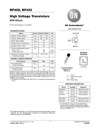
  • 1. BF420, BF422 High Voltage Transistors NPN Silicon • Pb−Free Package is Available* http://onsemi.com MAXIMUM RATINGS Rating Symbol BF420 BF422 Unit COLLECTOR 2 Collector −Emitter Voltage VCEO 300 250 Vdc Collector −Base Voltage VCBO 300 250 Vdc 3 Emitter −Base Voltage VEBO 5.0 Vdc BASE Collector Current − Continuous IC 50 mAdc 1 Collector Current − Peak ICM 100 mA EMITTER Total Device Dissipation (Note 1) PD @ TA = 25°C 830 mW Derate above 25°C 6.6 mW/°C MARKING Operating and Storage Junction TJ, Tstg −55 to +150 °C DIAGRAM Temperature Range THERMAL CHARACTERISTICS BF Characteristic Symbol Max Unit 42x 1 AYWW Thermal Resistance, RqJA °C/W 2 3 Junction to Ambient 150 Thermal Resistance, RqJL °C/W TO−92 (TO−226AA) Junction to Lead 68 CASE 29−11, STYLE 14 Maximum ratings are those values beyond which device damage can occur. Maximum ratings applied to the device are individual stress limit values (not normal operating conditions) and are not valid simultaneously. If these limits are x = 0 or 2 exceeded, device functional operation is not implied, damage may occur and A = Assembly Location reliability may be affected. Y = Year 1. Mounted on a FR4 board with 200 mm2 of 1 oz copper and lead length of WW = Work Week 5 mm. ORDERING INFORMATION Device Package Shipping† BF420ZL1 TO−92 2000 Ammo Pack BF422 TO−92 5000 Units/Box BF422G TO−92 5000 Units/Box (Pb−Free) BF422RL1 TO−92 2000 Tape & Reel BF422ZL1 TO−92 2000 Ammo Pack †For information on tape and reel specifications, including part orientation and tape sizes, please refer to our Tape and Reel Packaging Specifications Brochure, BRD8011/D. *For additional information on our Pb−Free strategy and soldering details, please download the ON Semiconductor Soldering and Mounting Techniques Reference Manual, SOLDERRM/D. © Semiconductor Components Industries, LLC, 2004 1 Publication Order Number: October, 2004 − Rev. 3 BF420/D
  • 2. BF420, BF422 ELECTRICAL CHARACTERISTICS (TA = 25°C unless otherwise noted) Characteristic Symbol Min Max Unit OFF CHARACTERISTICS Collector −Emitter Breakdown Voltage (Note 220 V(BR)CEO Vdc (IC = 1.0 mAdc, IB = 0) BF420 300 — BF422 250 — Collector −Base Breakdown Voltage V(BR)CBO Vdc (IC = 100 mAdc, IE = 0) BF420 300 — BF422 250 — Emitter −Base Breakdown Voltage V(BR)EBO Vdc (IE = 100 mAdc, IC = 0) BF420 5.0 — BF422 5.0 — Collector Cutoff Current ICBO µAdc (VCB = 200 Vdc, IE = 0) BF420 — 0.01 BF422 — — Emitter Cutoff Current IEBO nAdc (VEB = 5.0 Vdc, IC = 0) BF420 — 100 BF422 — — ON CHARACTERISTICS DC Current Gain hFE — (IC = 25 mAdc, VCE = 20 Vdc) BF420 50 — BF422 50 — Collector −Emitter Saturation Voltage VCE(sat) Vdc (IC = 20 mAdc, IB = 2.0 mAdc) — 0.5 Base −Emitter Saturation Voltage VBE(sat) Vdc (IC = 20 mAdc, IB = 2.0 mAdc) — 2.0 SMALL−SIGNAL CHARACTERISTICS Current Gain — Bandwidth Product fT MHz (IC = 10 mAdc, VCE = 10 Vdc, f = 20 MHz) 60 — Common Emitter Feedback Capacitance Cre pF (VCB = 30 Vdc, IE = 0, f = 1.0 MHz) — 1.6 2. Pulse Test: Pulse Width v 300 ms; Duty Cycle v 2.0%. http://onsemi.com 2
  • 3. BF420, BF422 120 VCE = 10 Vdc TJ = +125°C 100 hFE , DC CURRENT GAIN 80 25°C 60 40 −55°C 20 0 0.1 1.0 10 100 IC, COLLECTOR CURRENT (mA) Figure 1. DC Current Gain 100 80 BANDWIDTH (MHz) Ceb @ 1MHz 70 60 C, CAPACITANCE (pF) 10 50 f T, CURRENT−GAIN 40 1.0 Ccb @ 1MHz 30 TJ = 25°C VCE = 20 V 20 f = 20 MHz 0.1 10 0.1 1.0 10 100 1000 1.0 2.0 3.0 5.0 7.0 10 20 30 50 70 100 VR, REVERSE VOLTAGE (VOLTS) IC, COLLECTOR CURRENT (mA) Figure 2. Capacitance Figure 3. Current−Gain − Bandwidth 1.4 1.2 VCE(sat) @ 25°C, IC/IB = 10 VCE(sat) @ 125°C, IC/IB = 10 V, VOLTAGE (VOLTS) 1.0 VCE(sat) @ −55°C, IC/IB = 10 0.8 VBE(sat) @ 25°C, IC/IB = 10 VBE(sat) @ 125°C, IC/IB = 10 0.6 VBE(sat) @ −55°C, IC/IB = 10 VBE(on) @ 25°C, VCE = 10 V 0.4 VBE(on) @ 125°C, VCE = 10 V VBE(on) @ −55°C, VCE = 10 V 0.2 0.0 0.1 1.0 10 100 IC, COLLECTOR CURRENT (mA) Figure 4. ”ON” Voltages http://onsemi.com 3
  • 4. BF420, BF422 PACKAGE DIMENSIONS TO−92 (TO−226) CASE 029−11 ISSUE AJ NOTES: 1. DIMENSIONING AND TOLERANCING PER ANSI A B Y14.5M, 1982. 2. CONTROLLING DIMENSION: INCH. 3. CONTOUR OF PACKAGE BEYOND DIMENSION R IS UNCONTROLLED. R 4. LEAD DIMENSION IS UNCONTROLLED IN P AND BEYOND DIMENSION K MINIMUM. P L INCHES MILLIMETERS SEATING DIM MIN MAX MIN MAX PLANE K A 0.175 0.205 4.45 5.20 B 0.170 0.210 4.32 5.33 C 0.125 0.165 3.18 4.19 D 0.016 0.021 0.407 0.533 G 0.045 0.055 1.15 1.39 X X D H 0.095 0.105 2.42 2.66 G J 0.015 0.020 0.39 0.50 K 0.500 −−− 12.70 −−− H J L 0.250 −−− 6.35 −−− N 0.080 0.105 2.04 2.66 V C P −−− 0.100 −−− 2.54 R 0.115 −−− 2.93 −−− SECTION X−X V 0.135 −−− 3.43 −−− 1 N N STYLE 14: PIN 1. EMITTER 2. COLLECTOR 3. BASE ON Semiconductor and are registered trademarks of Semiconductor Components Industries, LLC (SCILLC). SCILLC reserves the right to make changes without further notice to any products herein. SCILLC makes no warranty, representation or guarantee regarding the suitability of its products for any particular purpose, nor does SCILLC assume any liability arising out of the application or use of any product or circuit, and specifically disclaims any and all liability, including without limitation special, consequential or incidental damages. “Typical” parameters which may be provided in SCILLC data sheets and/or specifications can and do vary in different applications and actual performance may vary over time. All operating parameters, including “Typicals” must be validated for each customer application by customer’s technical experts. SCILLC does not convey any license under its patent rights nor the rights of others. SCILLC products are not designed, intended, or authorized for use as components in systems intended for surgical implant into the body, or other applications intended to support or sustain life, or for any other application in which the failure of the SCILLC product could create a situation where personal injury or death may occur. Should Buyer purchase or use SCILLC products for any such unintended or unauthorized application, Buyer shall indemnify and hold SCILLC and its officers, employees, subsidiaries, affiliates, and distributors harmless against all claims, costs, damages, and expenses, and reasonable attorney fees arising out of, directly or indirectly, any claim of personal injury or death associated with such unintended or unauthorized use, even if such claim alleges that SCILLC was negligent regarding the design or manufacture of the part. SCILLC is an Equal Opportunity/Affirmative Action Employer. This literature is subject to all applicable copyright laws and is not for resale in any manner. PUBLICATION ORDERING INFORMATION LITERATURE FULFILLMENT: N. American Technical Support: 800−282−9855 Toll Free ON Semiconductor Website: http://onsemi.com Literature Distribution Center for ON Semiconductor USA/Canada P.O. Box 61312, Phoenix, Arizona 85082−1312 USA Order Literature: http://www.onsemi.com/litorder Phone: 480−829−7710 or 800−344−3860 Toll Free USA/Canada Japan: ON Semiconductor, Japan Customer Focus Center Fax: 480−829−7709 or 800−344−3867 Toll Free USA/Canada 2−9−1 Kamimeguro, Meguro−ku, Tokyo, Japan 153−0051 For additional information, please contact your Email: orderlit@onsemi.com Phone: 81−3−5773−3850 local Sales Representative. http://onsemi.com BF420/D 4
  • 5. This datasheet has been download from: www.datasheetcatalog.com Datasheets for electronics components.