Download as PDF, PPTX
![• Implementation specific DEBUG support can be identified by inspecting ROM Table
• Refer to previous slide (memory map) to get ROM table placement
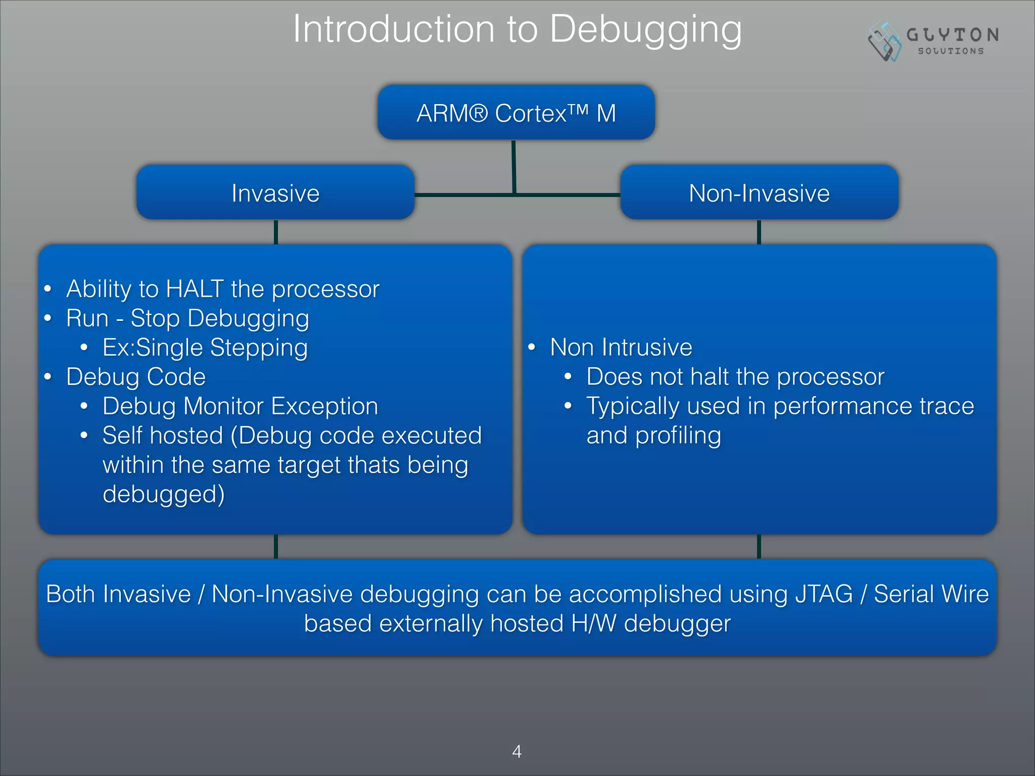
How to probe level of Debug Support ? ROM Table
Offset Value Name Description
0x000 0xFFF0F003 ROMSCS Points to the SCS at 0xE000E000.
0x004
0xFFF02002 or
0xFFF02003
ROMDWT
Points to the Data Watchpoint and Trace block at 0xE0001000.
Bit [0] is set to 1 if a DWT is fitted.
0x008
0xFFF03002 or
0xFFF03003
ROMFPB
Points to the Flash Patch and Breakpoint block at 0xE0002000.
Bit [0] is set to 1 if an FPB is fitted.
0x00C
0xFFF01002 or
0xFFF01003
ROMITM
Points to the Instrumentation Trace block at 0xE0000000.
Bit [0] is set to 1 if an ITM is fitted.
0x010
0xFFF41002 or
0xFFF41003
ROMTPIU
Points to the Trace Port Interface Unit. Bit [0] is set to 1 if a TPIU is
fitted and accessible to the processor on its PPB
0x014
0xFFF42002 or
0xFFF42003
ROMETM
Points to the Embedded Trace Macrocell block. Bit [0] is set to 1 if an
ETM is fitted and accessible to the processor on its PPB
0x018 0x00000000 END
End-of-table marker. It is IMPLEMENTATION DEFINED whether the table
is extended with pointers to other system debug resources. The table
entries always terminate with a null entry
• Above table mentions partial ROM table (Major Components) only
• An Implementation does not have to add support for all the above. For implementation specific
features, please refer to TRM from the respective silicon vendor](https://image.slidesharecdn.com/armcortexmbootupcmsispart33debugarchitecture-140824142714-phpapp01/75/ARM-Cortex-M-Bootup_CMSIS_Part_3_3_Debug_Architecture-7-2048.jpg)
![• BIT[0], of any entry in the ROM table, indicates whether
the implementation includes the respective block
• In case if BIT[0] confirms the inclusion of a specific
block , then DEBUG registers might provide additional
information regarding
!8
ROM Table — Key Take aways](https://image.slidesharecdn.com/armcortexmbootupcmsispart33debugarchitecture-140824142714-phpapp01/75/ARM-Cortex-M-Bootup_CMSIS_Part_3_3_Debug_Architecture-8-2048.jpg)

This document is the third part of a presentation on ARM Cortex-M bootup, system initialization, and the CMSIS interface, detailing debugging architectures and capabilities. It discusses both invasive and non-invasive debugging techniques, along with the architecture's specific debug components like DWT, ITM, and ETM. The presentation concludes by emphasizing the integration of on-board debugging tools like the Segger J-Link debugger with the EFM32 microcontroller.