GRAPHENE SYNTHESIS AND APPLICATION POSTERAman Gupta
For free download Subscribe to https://www.youtube.com/channel/UCTfiZ8qwZ_8_vTjxeCB037w and Follow https://www.instagram.com/fitrit_2405/ then please contact +91-9045839849 over WhatsApp.
Graphene eplained by poster presentation
GRAPHENE SYNTHESIS AND APPLICATION POSTERAman Gupta
For free download Subscribe to https://www.youtube.com/channel/UCTfiZ8qwZ_8_vTjxeCB037w and Follow https://www.instagram.com/fitrit_2405/ then please contact +91-9045839849 over WhatsApp.
Graphene eplained by poster presentation
Graphene, a single atom layer of Carbon, has amazing properties, that can be used in various fields such as flexible transparent touch screen, paper battery, ultra capacitor ect. Get an overall knowledge about what is graphene, its structure, synthesis, applications from this slides. Graphene technologies are creating a new era in the material science and hence in other sectors.
Electron transfer between methyl viologen radicals and graphene oxidekamatlab
Methyl viologen radicals are capable of transferring electrons to graphene oxide and partially restore the sp2 network. The reduced graphene oxide serves as a scaffold to anchor Ag nanoparticles. The growth of these silver nanoparticles is dictated by the ability of RGO to store and shuttle electrons. The RGO/Ag nanocomposites discussed in the present work offer new opportunities to design next generation photocatalysts.
Visit our website, KamatLab.com, for the latest news, publications, and research from our group.
PRESENTATION OUTLINE
Introduction,History of Nanotechnology,What is Nanotechnology, Definition of Nano,History of Graphene,Graphene,Why Nanotechnology,Size of Nanotechnology,What is Graphene, Properties of Graphene,Graphene Structure,Types of Graphene ,Synthesize Graphene,Applications,Conclusions,References
This presentation showcased first part of our work on graphene-based transistors as our final year project at NIT Patna under guidance of Prof.Wasim akram
Graphene: its increasing economic feasibility Jeffrey Funk
These slides use concepts from my (Jeff Funk) course entitled analyzing hi-tech opportunities to analyze how Graphene is becoming economic feasible for an increasing number of applications as its price falls and its quality/performance rises through improvements in chemical vapor deposition processes. Graphene is one of the strongest materials discovered, has high electronic and thermal conductivities, and unusual optical properties. These slides describe a number of applications for which Graphene is gradually becoming economically feasible including displays, integrated circuits, solar cells, water desalination, and natural gas tanks.
GRAPHENE SYNTHESIS AND ITS APPLICATIONS TERM PAPER PRESENTATIONAman Gupta
For free download Subscribe to https://www.youtube.com/channel/UCTfiZ8qwZ_8_vTjxeCB037w and Follow https://www.instagram.com/fitrit_2405/ then please contact +91-9045839849 over WhatsApp.
Graphene synthesis process and its current and future applications explained in brief
A short description about Graphene. Gives information about the discovery, properties, applications. This short file contains all the major information about graphene and appropriate references for further research.
Graphene is one the wonder materials in modern world,I Shaunak Bhattacharya with help of my group mates has made this presentation. Since I referred to slideshare.net for my presentation it was my duty to give it something back. I would be really happy if my presentation comes handy to anyone.
Simulation of AlGaN/Si and InN/Si ELECTRIC –DEVICESijrap
In this work, efficient solar-blind metal-semiconductor photodetectors grown on Si (111) by
molecular beam epitaxy are reported. Growth details are described,the comparison enters the
properties electric of InN/Si and AlGaN/Si photodectors with 0.2 μm of AlGaN and InN layers.
Modeling and simulation were performed by using ATLAS-TCAD simulator. Energy band
diagram, doping profile, conduction current density,I-V caracteristic , internal potential and
electric field were performed.
Simulation of AlGaN/Si and InN/Si ELECTRIC –DEVICESijrap
In this work, efficient solar-blind metal-semiconductor photodetectors grown on Si (111) by
molecular beam epitaxy are reported. Growth details are described,the comparison enters the
properties electric of InN/Si and AlGaN/Si photodectors with 0.2 µm of AlGaN and InN layers.
Modeling and simulation were performed by using ATLAS-TCAD simulator. Energy band
diagram, doping profile, conduction current density,I-V caracteristic , internal potential and
electric field were performed
Simulation Of Algan/Si And Inn/Si Electric - Devicesijrap
In this work, efficient solar-blind metal-semiconductor photodetectors grown on Si (111) by
molecular beam epitaxy are reported. Growth details are described,the comparison enters the
properties electric of InN/Si and AlGaN/Si photodectors with 0.2 µm of AlGaN and InN layers.
Modeling and simulation were performed by using ATLAS-TCAD simulator. Energy band
diagram, doping profile, conduction current density,I-V caracteristic , internal potential and
electric field were performed.
LGS crystal which melts congruently at 1470⁰C has been grown by Czochralski method. The langasite
crystal of length about 1cm grown along its Z-axis was cut in X and Y directions , polished and
subjected to various characterization studies. Phase and structure of the grown crystal was confirmed by
Powder XRD measurement. FTIR spectrum was carried out to confirm the functional groups present in
the grown crystals. The optical behavior was studied by UV–vis-NIR analysis. Electrical properties such as Dielectric constant, Resistivity, Conductivity and Piezoelectric coefficient have also been studied.
This to demonstrate the laser ablation of hard materials to form a thin film for optical sensors. The work was done at DIllard University , New Orleans LA by Professor Abdalla Darwish. any comment e-mail adarwish@bellsouth.net.
Scientific & Technological Perspective:
Future of Energy Storage With
Graphene Oxide (GO)
Paper Presentation
By
Radhey Shyam Meena
In
International Conference On
Advanced in Power Generation From
Renewable Energy Sources
APGRES 2015, June 15-16, 2015
Rajasthan Technical University Kota
Dr. Harold Weinstock presents an overview of his program, Quantum Electronic Solids, at the AFOSR 2013 Spring Review. At this review, Program Officers from AFOSR Technical Divisions will present briefings that highlight basic research programs beneficial to the Air Force.
The International Journal of Engineering & Science is aimed at providing a platform for researchers, engineers, scientists, or educators to publish their original research results, to exchange new ideas, to disseminate information in innovative designs, engineering experiences and technological skills. It is also the Journal's objective to promote engineering and technology education. All papers submitted to the Journal will be blind peer-reviewed. Only original articles will be published.
The papers for publication in The International Journal of Engineering& Science are selected through rigorous peer reviews to ensure originality, timeliness, relevance, and readability.
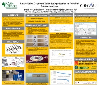
1. Reduction of Graphene Oxide for Application in Thin-Film
Supercapacitors
Davis Hu1, Ilia Ivanov2*, Mussie Alemseghed2, Michael Hu2
1Maryville College, Maryville, TN 37804 · 2Oak Ridge National Laboratory · *Mentor
ABSTRACT
ACKNOWLEDGMENTS
This work was supported by the Department of Energy Oak
Ridge National Laboratory and Oak Ridge Institute for
Science and Education under the Summer Undergraduate
Laboratory Internship program. I would like to thank my
mentor Ilia Ivanov for his mentorship. I would also like to
thank Mussie Alemseghed for providing GO synthesis.
Lastly, I would like to thank Michael Hu for his eye directing
vision for making this project possible.
BACKGROUND
RESEARCH QUESTION EXPERIMENTAL RESULTS AND DATA
MATERIALS/METHODS
• The goal of this project is to develop laser-based
reduction of GO for the design of advanced solid
state capacitors and flexible electronic circuits.
The reduction of GO was done using three lasers
(532, 633 and 785 nm) focused confocally
through a 20x, 50x and 100 x objectives on the
sample of GO deposited on the surface of a
glass slide.
EXPERIMENTAL RESULTS AND DATA
• Graphene Oxide (GO), an oxidized form of
graphene, is a single or multi-layered molecular
sheet synthesized from graphite crystals, have
recently been used in conductive transparent films
and other energy-related applications.
• The production of reduced rGO can be
accomplished by microwave, photo and laser
heating methods.
What is the optimized
conditions for the reduction of
Graphene Oxide using laser?
WHAT IS GO?
Figure 1. Molecular structure of graphene.
Reference: Openstax CNX www.cnx.org
Figure 2. Reduction process of graphite to GO to rGO.
Reference: The University of Turku www.utu.fi
MANAGING SUPPORT
Figure 3. Dispersed GO in alcohol can be printed on
flexible substrates and reduced to generate conductive
and dielectric circuits of the next generation.
• Glass slides were cleaned with alcohol prior to GO
deposition.
• X-Y-Z computer controlled sono-spray deposition
(SonoTek Exactacoat Ultrasonic Coating System) was
used to create 1, 2, 5, 10, 15, and 20 GO layers on the
glass slides
• Raman spectrum of GO is measured as a function of
irradiation time.
• A writable LightScribe supported Verbatim CD-R 52x
was obtained from mentor.
• GO was deposited using sono-spray increasing
number of layers from left to right. Square electrodes
were burned five times to achieve rGO.
• Conductivity is measured using four-point probe.
• Gold/Chrome electrodes were deposited onto quartz
slides containing GO.
• Wires were attached to the gold/chrome electrodes
using silver paste.
• GO is reduced to rGO using laser focused between
electrodes.
• The impedance of GO were measured as a function of
irradiation time.
UV-Visible Spectroscopy
•Technique to measure absorption or reflectance in the visible
range.
•Molecules undergo electronic transitions in the regions.
•π or non-bonding electrons absorb energy in the form of UV or
visible light to excite the electrons to higher anti-bonding
molecular orbitals.
Figure 4. A series of glass slides with 1, 2, 5,10,15 and 20
GO layers
Figure 5. Square rGO electrodes on CD
Raman Spectroscopy
•Raman spectroscopy is the common method to characterize
rate of reduction of graphene by determining information such
as disorder, edge and grain boundaries, thickness, doping,
strain and thermal conductivity under varying physical
conditions.
•The various conditions are: exposure time (1, 2, 3, 5, 10, 15,
20, 30, 60 min), laser wavelength (532, 633, 785 nm), objective
lens (20x, 50x, 100x), and power (1%, 10%, 100%)
•In graphene, the Stokes phonon energy shift caused by laser
excitation creates two main peaks in Raman spectrum: G (1580
cm-1), a primary in-plane vibrational mode, and 2D (2690 cm-1),
a second-order overtone of a different in-plane vibration, D
(1350 cm-1)
•The reduction of GO can be determined by plotting the ID/IG
Intensity Ratio vs. Time signifying an initial high peak of ratio
intensity followed by decrease in reduction.
Capacitance Using Cyclic Voltammetry
•Used a three electrode setup consisting of working, reference and
counter which are glassy carbon, Ag/AgCl, and Platinum
respectively.
Electrochemical Impedance Spectroscopy
•Dielectric properties of materials can be measured using
EIS. The measured frequency dependent impedance
response can be modeled using equivalent circuit model and
the capacitance element can be obtained.
CONCLUSIONS
Figure 6. Test structure for measuring kinetics of
GOrGO using impedance and Raman spectroscopy
• GO can be reduced to produce rGO with 532,
633, 785 nm lasers. The best laser for reduction
is at 633 nm.
• Raman D and G peaks are prominent at 532
(green) and 633 nm (red) but not for 785 nm
(purple) which explains that the Raman intensity
depends on the laser wavelength color.
• The maximum capacitance of GO was found to
be 2.70x10⁻³ F/g at 0.4 volts and 1.74 F/g at 0.7
volts in acetonitrile and NaOH respectively. The
value of the capacitance was calculated at a
range from 0.2 to 0.5 volts/sec and 0.25 to 1.00
volts/sec for acetonitrile and NaOH respectively.
• EIS and equivalent circuit modeling gave the
capacitance value of 7.88240-11 F.
GO in Alcohol Solution Flexible Electronics
GO
rGO
Reference: ScienceRay www.scienceray.com