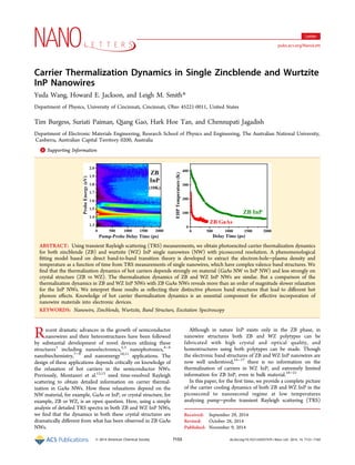
This document analyzes the carrier thermalization dynamics in single zincblende and wurtzite InP nanowires using transient Rayleigh scattering measurements with picosecond resolution. The results show that carrier thermalization depends strongly on the material (GaAs NW vs InP NW) and less strongly on crystal structure (ZB vs WZ). Specifically, thermalization is similar for ZB and WZ InP NWs, but is over an order of magnitude slower for InP NWs compared to ZB GaAs NWs. This difference is interpreted as reflecting the distinctive phonon band structures of the materials, which lead to different hot phonon effects during carrier cooling.
Electron Diffusion and Phonon Drag Thermopower in Silicon NanowiresAI Publications
The field of thermoelectric research has undergone a renaissance and boom in the fast two decades, largely fueled by the prospect of engineering electronic and phononic properties in nanostructures, among which semiconductor nanowires (NWs) have served both as an important platform to investigate fundamental thermoelectric transport phenomena and as a promising route for high thermoelectric performance for device applications. In this report we theoretical studied the carrier diffusion and phonon-drag contribution to thermoelectric performance of silicon nanowires and compared with the existing experimental data. We observed a good agreement between theoretical data and experimental observations in the overall temperature range from 50 – 350 K. Electron diffusion thermopower is found to be dominant mechanism in the low temperature range and shows linear dependence with temperature.
Direct detection of a break in the teraelectronvolt cosmic-ray spectrum of el...Sérgio Sacani
High-energy cosmic-ray electrons and positrons (CREs), which
lose energy quickly during their propagation, provide a probe of
Galactic high-energy processes1–7 and may enable the observation
of phenomena such as dark-matter particle annihilation or
decay8–10. The CRE spectrum has been measured directly up to
approximately 2 teraelectronvolts in previous balloon- or spaceborne
experiments11–16, and indirectly up to approximately 5
teraelectronvolts using ground-based Cherenkov γ-ray telescope
arrays17,18. Evidence for a spectral break in the teraelectronvolt
energy range has been provided by indirect measurements17,18,
although the results were qualified by sizeable systematic
uncertainties. Here we report a direct measurement of CREs in the
energy range 25 gigaelectronvolts to 4.6 teraelectronvolts by the
Dark Matter Particle Explorer (DAMPE)19 with unprecedentedly
high energy resolution and low background. The largest part of
the spectrum can be well fitted by a ‘smoothly broken power-law’
model rather than a single power-law model. The direct detection of
a spectral break at about 0.9 teraelectronvolts confirms the evidence
found by previous indirect measurements17,18, clarifies the behaviour
of the CRE spectrum at energies above 1 teraelectronvolt and sheds
light on the physical origin of the sub-teraelectronvolt CREs.
I show how much GW corrections are important not only for the band structure but also in the calculation of the electron-phonon matrix elements. I present different examples and comparison with the experimental results.
Prof Tom Trainor (University of Washington, Seattle, USA)Rene Kotze
TITLE: Two cultures in high energy nuclear physics
Since the mid eighties a community originating within the Bevalac program at the LBNL has sought to achieve formation of a color-deconfined quark-gluon plasma in heavy ion (A-A) collisions using successively higher collision energies at the AGS, SPS, RHIC and now the LHC, emphasizing a flowing dense "partonic" medium as the principal phenomenon. During much of the same period the high energy physics (HEP) community studying elementary collisions (e-e, e-p, p-p) developed the modern theory of QCD, emphasizing dijet production (fragmentation of scattered partons to observable hadrons) as the principal (calculable) phenomenon. Initially it was assumed that the QGP phenomenon in most-central A-A collisions might be distinguished from the HEP dijet phenomenon in elementary collisions. However, strong overlaps in phenomenology have revealed significant conflicts between QGP and HEP "cultures," especially at RHIC and LHC energies. In this talk I review some of the history and contrast an assortment of experimental evidence and interpretations from the two cultures with suggested conflict resolution.
Ultrasonic attenuation is a very important physical parameter to characterize the material, which is well associated to numerous physical quantities.An effort has been made for obtaining higher order elastic constants of CaO starting from basic parameters viz. nearest neighbor distance, hardness parameter and using Coulomb and Börn-Mayer potentials. These values are utilized to obtain Grüneisen parameters and non-linearity constants. Non-linearity constants ratio, ultrasonic attenuation due to phonon-phonon interaction (a/f2)p-p and thermo elastic loss (a/f2)th are calculated in a wide temperature range along <100>, <110> and <111> crystallographic directions of propagation for longitudinal and shear waves and compared with available theoretical and experimental results. From the attenuation values along different directions; it is evident that the ultrasonic attenuation is different along different directions of propagation and varies with the orientation of the crystal.
Air- and water-stable halide perovskite nanocrystals protected with nearly-mo...Pawan Kumar
Halide perovskites are exciting candidates for broad-spectrum photocatalysts but have the problem of ambient stability. Protective shells of oxides and polymers around halide perovskite nano- and micro-crystals provide a measure of chemical and photochemical resilience but the photocatalytic performance of perovskites is compromised due to low electron mobility in amorphous oxide or polymer shells and rapid charge carrier recombination on the surface. Herein an in situ surface passivation and stabilization of CsPbBr3 nanocrystals was achieved using monolayered graphenic carbon nitride (CNM). Extensive characterization of carbon nitride protected CsPbBr3 nanocrystals (CNMBr) indicated spherical CsPbBr3 nanoparticles encased in a few nm thick g-C3N4 sheets facilitating better charge separation via percolation/tunneling of charges on conductive 2D nanosheets. The CNMBr core-shell nanocrystals demonstrated enhanced photoelectrochemical water splitting performance and photocurrent reaching up to 1.55 mA cm−2. The CNMBr catalyst was successfully deployed for CO2 photoreduction giving carbon monoxide and methane as the reaction products.
Implementing Integrity: The Business Case for Forging an Ethical Company and ...Sean Cumberlege
This presentation advocates the need for extractive companies to commit to operating with integrity and recommends a more data driven and locally specific approach to identifying and mitigating social risk, including supply chain risk. The talk also frames social risk issues for an audience comprised mostly of attorneys.
International Journal of Engineering Research and Applications (IJERA) is an open access online peer reviewed international journal that publishes research and review articles in the fields of Computer Science, Neural Networks, Electrical Engineering, Software Engineering, Information Technology, Mechanical Engineering, Chemical Engineering, Plastic Engineering, Food Technology, Textile Engineering, Nano Technology & science, Power Electronics, Electronics & Communication Engineering, Computational mathematics, Image processing, Civil Engineering, Structural Engineering, Environmental Engineering, VLSI Testing & Low Power VLSI Design etc.
The Effect of RF Power on ion current and sheath current by electrical circui...irjes
Plasma is very important in the development of technology as it is applied in many electronic devices
such as global positioning system (GPS). In addition, fusion and process of plasma requires important elements,
namely, the electron energy distribution. However, plasma glow is a relatively new research field in physics.
There has not been found any previous study on the electric plasma modeling. Thus, this study was aimed to
study plasma modeling especially to find out what was the difference in the number of density and the
temperature of the electron in the plasma glow before and after heated and to discover how was the distribution
of electron and ion in the plasma. This research was conducted at Brawijaya University, Malang, Indonesia in
the Faculty of Science. This exploration began in the middle of June 2013. The data collection and data analysis
were done during a year around until August 2014. In this research, characteristics of plasma were studied to
build model of plasma. It utilized MATLAB dialect program examination framework which result in the
distribution of temperature and current density. The findings show that there has been a large increase in the
number of U, U2 with power, while figures of U1 is stable until middle of curve and then decrease as u but u2
after increase at point then stable. The differences appearing are probably due to the simplifying assumptions
considered in the present model. There was a curve between current in sheath and plasma. And time and sheath
current increased in the beginning then decreased before they experienced another increase.
International Journal of Engineering Research and Applications (IJERA) is an open access online peer reviewed international journal that publishes research and review articles in the fields of Computer Science, Neural Networks, Electrical Engineering, Software Engineering, Information Technology, Mechanical Engineering, Chemical Engineering, Plastic Engineering, Food Technology, Textile Engineering, Nano Technology & science, Power Electronics, Electronics & Communication Engineering, Computational mathematics, Image processing, Civil Engineering, Structural Engineering, Environmental Engineering, VLSI Testing & Low Power VLSI Design etc.
Transient Absorption Spectrometry in Photoelectrochemical Splitting of Water RunjhunDutta
Detailed Description of Application of Transient Absorption Spectrometry in Photoelectrochemical Splitting of Water for studying the electron-hole pair recombination in semiconductor.
[Illustrated with examples (Reference: Research Papers)]
International Journal of Engineering Research and Applications (IJERA) is an open access online peer reviewed international journal that publishes research and review articles in the fields of Computer Science, Neural Networks, Electrical Engineering, Software Engineering, Information Technology, Mechanical Engineering, Chemical Engineering, Plastic Engineering, Food Technology, Textile Engineering, Nano Technology & science, Power Electronics, Electronics & Communication Engineering, Computational mathematics, Image processing, Civil Engineering, Structural Engineering, Environmental Engineering, VLSI Testing & Low Power VLSI Design etc.
Artigo que descreve o trabalho feito com o Chandra nos aglomerados de galáxias de Perseus e Virgo sobre a descoberta de uma turbulência cósmica que impede a formação de novas estrelas.
International Journal of Engineering Research and Applications (IJERA) is an open access online peer reviewed international journal that publishes research and review articles in the fields of Computer Science, Neural Networks, Electrical Engineering, Software Engineering, Information Technology, Mechanical Engineering, Chemical Engineering, Plastic Engineering, Food Technology, Textile Engineering, Nano Technology & science, Power Electronics, Electronics & Communication Engineering, Computational mathematics, Image processing, Civil Engineering, Structural Engineering, Environmental Engineering, VLSI Testing & Low Power VLSI Design etc.
the paper focuses on the fabrication and characterization of heterostructures using transition metal dichalcogenide (TMDC) monolayers. The authors describe the process of mechanical exfoliation to obtain thin flakes of TMDC material, which are then placed on a viscoelastic polydimethylsiloxane film. These monolayers are subsequently stamped onto a silicon wafer covered with thermal oxide to create heterobilayers .
The paper also discusses the use of ultrafast optical-pump/terahertz-probe near-field microscopy to study these heterostructures. The authors explain that this technique allows them to investigate the electric near fields and scattered fields of the emitted waveforms, as well as the photo-induced polarizability .
The experimental setup involves a high-average-power, low-noise Yb:YAG thin-disc oscillator, which generates terahertz probe pulses through optical rectification of 200-fs-long pulses. These pulses are centered at a wavelength of 1,030 nm and are generated in a gallium phosphide crystal .
The paper likely includes additional details on the experimental procedures, data analysis, and results obtained from the terahertz near-field microscopy experiments. It may also discuss the potential applications and implications of the findings
Optical and Impedance Spectroscopy Study of ZnS NanoparticlesIJMER
International Journal of Modern Engineering Research (IJMER) is Peer reviewed, online Journal. It serves as an international archival forum of scholarly research related to engineering and science education.
International Journal of Modern Engineering Research (IJMER) covers all the fields of engineering and science: Electrical Engineering, Mechanical Engineering, Civil Engineering, Chemical Engineering, Computer Engineering, Agricultural Engineering, Aerospace Engineering, Thermodynamics, Structural Engineering, Control Engineering, Robotics, Mechatronics, Fluid Mechanics, Nanotechnology, Simulators, Web-based Learning, Remote Laboratories, Engineering Design Methods, Education Research, Students' Satisfaction and Motivation, Global Projects, and Assessment…. And many more.
2. measurements by expanding the analysis of Montazeri et al.12,13
to include complex multiband structures. For instance, in WZ
InP NWs, relaxation dynamics must include both electron
thermalization in a single conduction band, as well as holes in
three separate valence bands: the A (heavy hole), B (light
hole), and C bands,15,16,23
which are separated by energies
determined by the spin−orbit and crystal-field interactions.22
To interpret the experimental results, we develop a simple
formalism based on direct band−band theory, which can model
the changes in the real and imaginary parts of the index of
refraction when the bands are dynamically occupied by carriers.
The many-body effects are included phenomenologically. We
extract the electron−hole density and temperature as a function
of time for each polytype for all bands, as well as their energy
positions. We then provide a phenomenological explanation of
the contrasting dynamics of InP and GaAs NWs by considering
hot phonon effects.
TRS Experimental Results and Spectra Fitting Model.
These measurements are performed on single MOCVD grown
ZB or WZ InP NWs at 10 K. The single phase ZB or WZ InP
NWs are nominally 150 nm in diameter. The ZB NWs were
intentionally doped by a low Si-doping concentration of
approximately 1016
cm−3
(deduced from TRS data analysis),
whereas the WZ NWs were undoped. In these TRS
experiments, the polarization of a tunable probe pulse (1.2−
2.0 eV) oscillates between parallel and perpendicular to a single
nanowire at 100 kHz using a photoelastic modulator (PEM).
Using a balanced detector the backscattered probe pulse is
monitored by a lockin amplifier tuned to the 100 kHz PEM
oscillator. This provides the signal which is the polarized
scattering efficiency: R′ = R∥ − R⊥. Using a pump pulse (at 2.25
eV), carriers are photoexcited into the wire which changes the
real and imaginary part of the index of refraction which in turn
changes the polarized scattering efficiency, R′. Both pump and
probe laser pulses have a width of ∼200 fs. The pump is
modulated on and off by a mechanical chopper at 773 Hz. By
looking at the change of R′ when pump is on and off, we
acquired ΔR′, which is a derivative-like structure and is much
sharper than R′. Moreover, the ΔR′ is measured at different
time delays of the probe after the initial pump by adjusting the
length of the time delay line in the probe laser path. With such
an experimental setup, we can measure the relative change of
the polarized Rayleigh scattering efficiency ΔR′/R′ as a
function of both probe energy and probe delay time after the
pump.
Typical spectra from a single ZB InP NW are shown in
Figure 1b, and the spectra map is plotted as a function of time
in Figure 1a. The false color in the TRS map represents the
value of ΔR′/R′, with red showing positive and blue showing
negative changes in the scattering efficiency R′, where R′ is the
linear dichroism (R∥ − R⊥). The derivative-like structure
becomes very sharp at late times when the carrier occupation
densities and temperatures are low, and so the energy position
of the fundamental band to band transition is seen with high
accuracy. The zero crossing point of the TRS spectrum is a
direct measure of the energy associated with a direct band-to-
band transition. The ZB InP NW band gap Eg is observed at
1.42 eV corresponding to an optical transition between the
degenerate light-hole (LH) and heavy hole (HH) bands and
the conduction band, whereas the corresponding transition
between the split-off (SO) band to the conduction band is
observed at 110 meV higher energy. Both of the results are in
excellent agreement with previous reports.23−26
The ΔR′/R′
spectral map (Figure 1a) at early times displays a more intense
response (larger changes in R′) and exhibits an increased
energy width and is centered at a higher energy compared to
later times. At very early times (t < 100 ps), the broadening
effects are strong enough to cause overlapping responses
between the higher lying SO-e transition and the lower lying
LH- and HH-e band edge. Perhaps more surprisingly, a very
weak transition is also observed around 1.95 eV, which may be
associated with the Γ−L transition between the top of the
valence band and the conduction band L-valley.
To model these light scattering lineshapes, we calculate ΔR′/
R′ based on the direct band-to-band transitions theory where
the bands are occupied by hot electrons and holes. The
absorption coefficient α[E, N, T] (Figure 2a) is calculated as a
function of carrier density and temperature through27
∫α
π
π
ρ ρ Ε
Ε
= ′ × ′ −
× − − ′ − ′ ′
−
E N T
c h
n E
B E E
f E E f E E
[ , , ]
(2 )
[ ] [ ]
( [ ] [ ])d
E E
c V
l g u
2 2 3
2 2 3
0
g
where n is the average index of refraction; B is the radiative
bimolecular coefficient which depends on the transition matrix
Figure 1. ZB InP NW TRS results and fits. (a) False color map of
ΔR′/R′ data, as a function of pump−probe delay time and probe
energy (red−positive, blue−negative). The band edge transitions can
be resolved at late times (∼2 ns) and are consistent with
measurements by other methods. The early time signal is broadened
and shifted toward higher energy primarily due to band filling effects.
The signal decay evolution is clear when one moves from early to late
times. (b) Selected ΔR′/R′ vs energy spectra (dots are measurements)
for times after pump pulse of 20 ps (red), 200 ps (green), and 2000 ps
(blue) as well as fitting (solid) curves based on direct band to band
transition theory. The EHP density and temperature in all bands are
revealed through this analysis (e.g., at 20/200/2000 ps after initial
excitation, the electron densities are 1 × 10¹⁸
/8 × 1017
/8 × 1016
cm−3
and temperatures are 384/252/60 K, respectively).
Nano Letters Letter
dx.doi.org/10.1021/nl503747h | Nano Lett. 2014, 14, 7153−71607154
3. element; ρi[E] is the 3D density of states in the conduction/
valence band; fi[E] = (1/(1 + exp[(E − EF)/(kBT)])) is the
Fermi−Dirac distribution probability that upper/lower states
involved in the transition are occupied by electrons, with the
quasi-Fermi energy EF[N, T] related to both the carrier density
N and temperature T; E′ is the upper state energy above the
conduction band minimum. For n and B, we use the average
values from the literature28−35
because only the relative change
of the absorption coefficient is critical, not its absolute value.
Using the Kramers−Kronig relation, we transform the
calculated absorption coefficient α[E, N, T] to obtain the
index of refraction n[E, N, T] as a function of carrier density
and temperature. We define the complex refractive index n = n
+ ik, where the extinction coefficient k = (λ/(4π))α. As shown
by Montazeri et al.,13
the line shape ΔR′/R′ is the direct
product of a complex phase factor eiθ
containing NW
geometrical information and the change of the complex index
of refraction Δn = Δn + iΔk. We therefore can write
Δ
Δ Δα
λ
π
θ Δ
λ
π
θ Δα
′
′
= +
= −
θ⎜ ⎟
⎛
⎝
⎞
⎠
{ }
R
R
Ae n i
A n
4
cos[ ]
4
sin[ ]
i
where A is an overall arbitrary amplitude factor. In Figure 2 we
show the resulting coefficients α, n, Δα, Δn and ΔR′/R′ for the
HH-e optical transition corresponding to fits of the ZB InP
TRS spectra at various times.
The final fitting curve is simply the superposition of each
ΔR′/R′ curve for transitions from each of the three valence
bands to the conduction band using the following assumptions:
(1) the temperature of the electrons and holes are the
same36−38
(i.e., they are thermalized with each other through
rapid (<1 ps) carrier−carrier scattering after initial excitation);
(2) the sum of the hole densities in all 3 valence bands (HH,
LH, SO for ZB/A, B, C for WZ) equals the density of electrons
in the conduction band (i.e., charge neutrality is assumed); (3)
the background density without pump excitation is 1015
cm−3
(i.e., the probe pulse itself excites a few carriers), which means
that separate quasi-Fermi energies are defined for each band
even if we assume the pump-excited holes are in thermal
equilibrium between various hole bands; (4) the background
temperature for these measurements is 10 K; (5) the amplitude
factor A and bimolecular coefficient B are the same if similar
electronic selection rules39,40
exist among different transitions
(the HH-e transition intensity dominates over LH-e or SO-e in
ZB InP, because the HH mass dominates23,41
where density of
states effective mass is one of the prefactors of n and α, which
turn out to be the component of the modeled ΔR′/R′); (6)
band-gap-renormalization (BGR) effects42,43
occur due to the
many-body-effects of the EHP and are treated as a free time-
dependent fitting parameter causing a rigid shift in the band
gap.
To fit the entire TRS spectra as a function of time, we
optimize all the parameters by running iteration cycles. Within
each cycle, we keep time-independent parameters fixed but
tune and optimize time-dependent parameters to acquire the
best fits for all the spectra. Those time-dependent parameters
are carrier densities, common carrier temperatures and the
BGR coefficients. The time-independent parameters are the
band gap, SO split-off energy, amplitude factors, and NW
geometry phase factor as well as the background density and
temperature. After one cycle is finished, we adjust time-
independent parameters slightly and start another iteration
cycle. By continually comparing the fitting results from different
iterations, we finally acquire the optimized time-independent
parameters as well as the corresponding time-dependent
parameters. The results of these fits are selectively shown at
several times after the pump pulse in Figure 1b. The fitted band
gap for ZB InP NW is 1.419 ± 0.001 eV and the split-off band
is 0.108 ± 0.001 eV below the top of the valence band. These
transition energies agree well with previous reports23−26
and
direct observations of the derivative structures at late times
(Figure 1a). The fitted phase factor result indicates the
diameter of the NW is approximately 160 nm based on the
relation between phase factor and nanowire diameter.12
In
analyzing the fits to the ΔR′/R′ spectrum, we find that the
intensity is primarily related to the hot carrier concentration,
whereas the spectral width is primarily related to the hot carrier
temperature and band filling. As a result of these effects, the
scattering lineshapes can overlap strongly at early times when
both the density and temperatures are high. This overlap shows
up, for instance, for the ZB InP Eg + Δso transition near 100 ps
where both the intensity and energy appear to drop. This
Figure 2. (a) and (b) Solid lines show the calculated absorption coefficient α[E] and index of refraction n[E] as a function of energy at different
times (20, 200, and 2000 ps shown as red, green and blue respectively) after initial pump-excitation obtained from the spectral line shape fitting
displayed in Figure 1b. The background αo[E] and no[E] (dashed) are calculated with no pump-photoexcitation but only probe-excitation (i.e., log
No = 1015
cm−3
, To = 10 K). (c) and (d) Change of the absorption coefficient Δα[E] and index of refraction Δn[E] at different times after initial
pump with respect to background αo and no. (e) The final Rayleigh scattering efficiency ((ΔR′)/R′) ∝ (Δn + iΔα(λ/(4π))) eiθ
is represented as a
direct product of the complex index of refraction and complex phase factor related to the nanowire geometry.
Nano Letters Letter
dx.doi.org/10.1021/nl503747h | Nano Lett. 2014, 14, 7153−71607155
4. structure results from the superposition of the spectral
lineshapes at Eg and Eg + Δso. At the earliest times, the band
gap renormalization tend to reduce the band gap slightly but
the strong band filling effects eventually cause the ΔR′/R′
structure move to higher energy. Due to the small electron
effective mass compared to holes, this band filling effect is
dominated by the pump-modulated electron distribution in the
conduction band.
Similar TRS measurements have been carried out on a single
MOCVD grown 150 nm diameter undoped WZ InP NW at
pump excitation intensity 4 × 10⁵
kW cm−2
, as displayed in
Figure 3a. By looking at the zero point of the derivative-like
structure at late times, the WZ InP NW Eg is observed at ∼1.49
eV which is the energy of the optical transition between the A
valence band and the conduction band, whereas the B valence
band to conduction band transition is observed ∼30 meV
higher in energy, and the C valence band to conduction band
transition is seen ∼160 meV higher in energy. At a larger pump
excitation intensity 2 × 10⁶
kW cm−2
, the A and B valence band
to second conduction band can be resolved at 1.74 and 1.77 eV
(see Supporting Information Figure S1). These results are in
excellent agreement with recent reports.15,16,22,44
Similar band
filling behavior to that observed in ZB InP is also seen in the
WZ InP NWs. We use the same fitting model based on direct
band-to-band transition theory to extract the WZ InP NW EHP
density and temperature as a function of time. One difference
for the WZ InP TRS data fitting model is that the A−e
transition intensity is extremely weak compared with B−e or
C−e. The reason for this is that the A−e transition is only
allowed for an electric-field polarized perpendicular to the WZ
InP c axis (NW long-axis), but this field is suppressed by the
dielectric contrast between the NW (150 nm diameter much
smaller than the laser wavelength ∼800 nm) and the
surrounding media (vacuum). The results of these fits are
shown at several times after the pump pulse in Figure 3b. The
fitted A, B, C-valence band to conduction band energies for WZ
InP are 1.485 ± 0.005 eV, 1.523 ± 0.005 eV, and 1.654 ± 0.005
eV, respectively, which agree well with previous reports15,16
and
direct observations of the derivative structures at late times
(Figure 3a). The fitted phase factor result gives an approximate
NW diameter of 160 nm based on the relation between phase
factor and nanowire diameter;12
the average diameter of NWs
measured by TEM for this growth is about 150 nm.22
EHP Density and Temperature Relaxation. With the
dynamics of carrier density and temperature obtained from the
fits to the TRS spectra, we can now plot the carrier population
density distribution versus time for all conduction and valence
bands. These are displayed in Figure 4a for ZB InP and Figure
5a for WZ InP. We assume that the background carrier density
without pump excitation is 1015
cm−3
, so at late times when the
carrier temperature is low, the occupation of the SO (for ZB)
or B, C (for WZ) valence bands is still observable. For the same
reason, the quasi-Fermi energy for each band is computed
individually from carrier density and temperature (with Fermi−
Dirac distribution and 3D density of states) in spite of the
assumption that pump excited holes in different hole bands are
in thermal equilibrium, which means each hole band’s quasi-
Fermi energies should be equal. The fact that the quasi-Fermi
energy is usually within kBT of the band edge supports our
assumption that the pump-excited carriers in the NWs are a
degenerate EHP, and thus, we can ignore excitonic effects.
The EHP density and temperature obtained from these fits as
a function of time are plotted in Figures 4b, c and 5b, c. The
carrier density and temperature of the ZB InP NW is 1.5 × 10¹⁸
cm−3
and 400 K at t = 0, which relaxes to 7.5 × 10¹⁶
cm−3
and
70 K by 2 ns. In contrast, the carrier density and temperature of
the WZ InP NW is 2 × 10¹⁷
cm−3
and 270 K at t = 0 which
relaxes to 2 × 10¹⁶
cm−3
and 50 K by 2 ns. The difference of the
initial carrier density and temperature reflects the fact that the
pump excitation intensity for the ZB NW was 1.2 × 10⁶
kW
cm−2
, whereas the WZ NW intensity was lower at 4 × 10⁵
kW
cm−2
. The larger excitation intensity is also reflected by the fact
that the ZB electron quasi-Fermi energy is above the
conduction band edge at the earliest times, whereas the WZ
electron quasi-Fermi energy is close to the conduction band
edge. Similarly, the BGR of ZB InP NW is larger than WZ InP
due to the higher EHP density.
To model the dynamics of the EHP carrier density, we
include both linear (nonradiative) and bimolecular (radiative)
recombination processes ignoring the background density from
either unintentional doping or probe excitation. We describe
the decay of the EHP density based on the sum of linear and
bimolecular recombination by dN/dt = −N/τ − BN2
and
obtain the nonradiative lifetime τ and bimolecular coefficient B
for both ZB and WZ InP NWs. For the ZB InP NWs, τ ∼ 1.4
ns and B ∼ 2 × 10⁻⁹
cm−3
s−1
; whereas for the WZ InP NWs, τ
∼ 3.4 ns and B ∼ 11 × 10−9
cm−3
s−1
. These values compare
reasonably well with previous reports,29−35,45,46
taking into
account that both parameters are strongly affected by sample
quality, temperature, and excitation carrier density. With the
knowledge of τ and B, the density loss rate through both
recombination mechanisms can be extracted. The values of the
different loss rates as a function of time are plotted in the insets
of Figures 4b and 5b. Dividing the radiative recombination rate
Figure 3. WZ InP nanowire TRS results and fits: (a) False color map
of ΔR′/R′ data as a function of pump−probe delay time and probe
energy (red−positive, blue−negative), (b) Selected ΔR′/R′ spectra
(dots are measurements) as well as fitted (solid) curves based on
direct band-to-band transition theory.
Nano Letters Letter
dx.doi.org/10.1021/nl503747h | Nano Lett. 2014, 14, 7153−71607156
5. by the total recombination rate, we get the percentage of the
carriers that recombine radiatively, or the internal quantum
efficiency, as a function of time (see Supporting Information
Figure S2). The average value of quantum efficiency over 0−2
ns is 62% for ZB and 78% for the WZ InP NWs.
Carrier Thermalization Dynamics: “Hot” Phonon
Effects. The EHP temperature is related to the total carrier
energy through the relation
η
η
=E k T
F
F
3
2
( )
( )
B
3
2
1
2
where η is the quasi-Fermi energy and Fi(η) is the ith Fermi
integral defined as usual. The decrease of carrier temperature is
due to carrier energy loss. Usually the most significant energy
loss mechanism for III−V semiconductors at higher carrier
temperatures is phonon scattering with longitudinal optical
(LO) phonon emission. At lower carrier temperatures, when
Figure 4. ZB InP nanowire TRS data fit results. (a) Electron−hole population density distributions, including quasi-Fermi energies (dashed and
dotted) and BGR (solid) in both conduction and valence bands as a function of time. (b) EHP density fit results (dots) as a function of time, with
the red curve modeled by a sum of linear and bimolecular recombination processes. The inset shows the separate recombination rates. (c) EHP
temperature fit results (dots) as a function of time, with the red curve modeled by optical and acoustic phonon scattering mechanisms. The inset
shows the energy loss rates due to optical or acoustic phonon emission.
Figure 5. WZ InP nanowire TRS data fit results. (a) Electron−hole population density distributions, including quasi-Fermi energies (dashed and
dotted) and BGR (solid) in the conduction and valence bands as a function of time. (b) EHP density fit results (dots) as a function of time, with the
red curve modeled by a sum of linear and bimolecular recombination processes. The inset shows the separate recombination rates. (c) EHP
temperature fit results (dots) as a function of time, with the red curve modeled by optical and acoustic phonon scattering mechanism. The inset
shows the energy loss rates due to optical or acoustic phonon emission.
Nano Letters Letter
dx.doi.org/10.1021/nl503747h | Nano Lett. 2014, 14, 7153−71607157
6. the majority of carriers have energies below the LO phonon
energy, acoustic-deformation potential (ADP) scattering with
acoustic phonon emission is dominant.36−38,47−49
Whether the
optical or acoustic phonon emission dominates the energy loss
rate (ELR) depends on both the carrier distribution and the
phonon band structures, i.e. the LO, LA and TA phonon
energies and density of states.
Examining the ZB InP NW energy loss rate (ELR)
(displayed in Figure 4c inset), we find that the optical phonon
ELR only slightly surpasses the acoustic phonon ELR at the
earliest times, after which acoustic phonon ELR dominates.
This contrasts with what is found in ZB GaAs13
where the
optical phonon ELR is more than an order of magnitude larger
than the acoustic phonon ELR in the first 100 ps, after which
acoustic phonon ELR dominants. Thus, the overall carrier
thermalization in the ZB InP NW is much slower than observed
in the ZB GaAs NW, as is clearly observable in Figure 6a. At
late times, when acoustic phonon ELR dominates, the larger
effective hole mass means that the relaxation will be dominated
by the interaction of the acoustic phonons with holes47−49
(see
Supporting Information Figure S3). We fit the temperature and
find that the ZB InP NW hole acoustic-deformation potential is
2.0 eV, which compares reasonably with previous reports
considering its temperature dependence.50−53
The distinctive difference between ZB GaAs and ZB InP NW
optical phonon ELR can be modeled by an carrier−LO phonon
Fröhlich coupling efficiency α introduced in the ELR equation
α= +
E
t
E
t
E
t
d
d
d
d
d
dLO ADP
As references 36−38,47−49,54,55 suggest, the LO phonon
scattering ELR reduction is usually observed in transient
measurements at highly excited (∼1018
cm−3
) semiconductors.
Because this phenomenon does not exist in steady-state
measurements or theoretical calculations based on Fröhlich
interaction at the same temperature, previous reports36,54
attribute this phenomenon to the nonequilibrium or “hot”
phonon effects. When the phonon temperature is elevated such
that hot carriers’ phonon emitting process begins to be
compensated by the carriers’ reabsorption of the hot phonons,
the final LO phonon scattering ELR will be greatly reduced
when the nonequilibrium phonon temperature approaches the
carrier temperature.
The values of the Fröhlich coupling efficiency α for ZB GaAs
and ZB InP NWs are found to be αZB GaAS
= 3 × 10⁻³
and
αZB InP
= 6 × 10⁻⁵
, respectively. The reason that hot phonon
effects appear much stronger in ZB InP relative to ZB GaAs is
that their phonon band structures are significantly different (see
Figure 6b, c), which implies a different pathway for LO phonon
relaxation. After the initial pump pulse excitation, a non-
equilibrium population of electrons and holes is relaxed initially
and most rapidly by the emission of LO phonons. These LO
phonons, in turn, usually decay into two acoustic phonons with
equal energy and opposite momentum, for example, LO → LA
+ LA, which is the case for ZB GaAs. In contrast, ZB InP has a
large phonon band gap such that the LO(Γ) energy (10.5 THz)
is more than twice the highest available acoustic phonon energy
(4.8THz, LA at the L-points). Thus, the ZB InP zone-center
LO → LA + LA decay is not allowed. Instead, the ZB InP LO
phonon must take a two-step process, that is, LO → TO + TA/
LA, then TO → LA(L) + LA(L), where the TO phonon energy
(9.4 THz) is close to twice of the LA(L) phonon energy (4.8
THz). The ZB InP zone-center TO decay lifetime is
reported56−58
to be a factor of 1−2 longer than ZB GaAs
zone-center LO phonon lifetime. The two-step processes
suggest an even longer LO phonon relaxation for InP compared
to the one-step process for GaAs LO phonon relaxation, which
is consistent with the observation58
that the ZB InP zone-center
LO phonon lifetime is a factor of 3−4 longer than that of ZB
GaAs at various temperatures. Thus, the total ZB InP carrier
energy loss through LO phonon emission per unit time is
expected to be smaller than for ZB GaAs and the carrier cooling
is expected to be slower. We believe that this qualitatively
explains the fact that the initial temperature relaxation of the
carriers though LO phonon scattering mechanism in ZB InP is
almost 50 times less efficient than is observed in ZB GaAs. A
detailed calculation of the LO phonon lifetime and Fröhlich
coupling efficiency α is beyond the scope of this paper due to
the complexity of the phonon emission and reabsorption
dynamics.
Interestingly, for ZB InP NWs, we observe a signature at
∼1.95 eV (Figure 1a), which is about the energy of the valence
band Γ-point to conduction band L-valley indirect transi-
tion.59−66
We did not observe any signs of indirect transitions
in ZB GaAs NW. In highly excited WZ InP NW, we only
observe a weak response from the direct transition between
valence band and second conduction band, which is zone-
folded from the L-valley.67
Hence the indirect transition should
be less efficient and hard to observe. For ZB InP NWs, with the
help of the LA(L) zone-edge phonons generated by hot zone-
center LO phonon two-step decay process, the probe laser can
relatively efficiently create indirect transitions thus causing a
change in the scattering efficiency R′ due to more absorption.
Using the energy of the absorbed LA(L) phonon of 20 meV,
we find the Γ−L indirect gap measured here is 1.97 eV, which is
Figure 6. (a) EHP temperature relaxation of ZB GaAs and ZB and
WZ InP. The sharp contrast of early time temperature decay through
LO phonon scattering is due to the distinction between (b) GaAs
phonon band structure (adapted from Giannozzi et al.69
) and (c) InP
phonon band structure (adapted from Fritsch et al.72
).
Nano Letters Letter
dx.doi.org/10.1021/nl503747h | Nano Lett. 2014, 14, 7153−71607158
7. in the range of previous reports 1.94−2.2 eV at low
temperatures.59−66
Looking at the WZ InP NW ELR (Figure 5c inset), we find
that the ratio of the initial ELR by LO and acoustic phonon
scattering is similar to ZB InP NW, but still much less than that
of ZB GaAs NWs. This is reflected by the value of the WZ InP
NWs Fröhlich coupling efficiency αWZ InP
= 5.4 × 10⁻⁵
. The
WZ InP hole acoustic-deformation potential, fitted through a
similar process as ZB InP, is found to be ∼2 eV, which agrees
with bulk ZB InP results.50−53
Although there is no direct
report of WZ InP LO phonon decay lifetimes either
experimentally (recall that WZ InP does not exist in bulk
form) or theoretically, we can still interpret this result using the
same phenomenological decay channel framework as detailed
above for ZB InP. For instance, the WZ InP phonon band
structures at Γ−A dispersion along [0001] can be roughly
approximated59
by folding the ZB InP Γ−L of the phonon
band structure along [111]. The phonon states are now
distributed closer to the zone-center, but the top of the acoustic
branches should be still at exactly the same energy as ZB InP
and the dispersion of LO/TO branches would not change due
to the flat dispersion nature of the optical branches. Hence, the
direct LO → LA + LA process is still not allowed for WZ InP
and a similar two-step process like that of ZB InP is required.
For that reason, we would expect a similar hot phonon effect
for WZ InP NW and thus a similarly slow thermalization
process as in ZB InP NW, in agreement with our observations.
Conclusions. Using time-resolved Rayleigh scattering, we
have directly measured the density and temperature relaxation
of optically excited electron−hole plasma in single ZB and WZ
InP nanowires. We demonstrate that a simple analysis
technique enables the extraction of the electron and hole
density and temperature in complex multiband materials.
Compared with similar measurements of ZB GaAs nanowires,
we find that the thermalization time of the EHP is nearly 50
times longer in ZB InP nanowires. This slower thermalization is
likely caused by the substantially different phonon band
structure of InP compared to GaAs, which inhibits the direct
relaxation of optical to acoustic phonons. Both ZB InP
nanowires and WZ InP nanowires have similar thermalization
dynamics. Information on the dependence of carrier thermal-
ization dynamics in different materials and nanostructures is an
essential component for the design of high efficiency nanowire
devices.
■ ASSOCIATED CONTENT
*S Supporting Information
An additional WZ InP TRS spectrum is provided, showing
excitations to the second conduction band, as well as more
detail on the ELR for electron and hole bands separately. This
material is available free of charge via the Internet at http://
pubs.acs.org.
■ AUTHOR INFORMATION
Corresponding Author
*E-mail: leigh.smith@uc.edu.
Notes
The authors declare no competing financial interest.
■ ACKNOWLEDGMENTS
We acknowledge the financial support of the National Science
Foundation through grants DMR-1105362, 1105121, and
ECCS-1100489 and the Australian Research Council. The
Australian National Fabrication Facility is acknowledged for
access to the growth facilities used in this research.
■ REFERENCES
(1) Yang, P.; Yan, R.; Fardy, M. Nano Lett. 2010, 10, 1529−1536.
(2) Cui, Y.; Lieber, C. M. Science 2001, 291, 851−853.
(3) Huang, Y.; Duan, X.; Cui, Y.; Lauhon, L. J.; Kim, K. H.; Lieber, C.
M. Science 2001, 294, 1313−1317.
(4) Huang, Y.; Duan, X.; Lieber, C. M. Small 2005, 1, 142−147.
(5) Qian, F.; Gradecak, S.; Li, Y.; Wen, C.-Y.; Lieber, C. M. Nano
Lett. 2005, 5, 2287−2291.
(6) Minot, E. D.; Kelkensberg, F.; van Kouwen, M.; van Dam, J. a;
Kouwenhoven, L. P.; Zwiller, V.; Borgström, M. T.; Wunnicke, O.;
Verheijen, M. a; Bakkers, E. P. a M. Nano Lett. 2007, 7, 367−371.
(7) Cui, Y.; Wei, Q.; Park, H.; Lieber, C. M. Science 2001, 293,
1289−1292.
(8) Zheng, G.; Patolsky, F.; Cui, Y.; Wang, W. U.; Lieber, C. M. Nat.
Biotechnol. 2005, 23, 1294−1301.
(9) Robinson, J. T.; Jorgolli, M.; Shalek, A. K.; Yoon, M.-H.; Gertner,
R. S.; Park, H. Nat. Nanotechnol. 2012, 7, 180−184.
(10) Chan, C. K.; Peng, H.; Liu, G.; McIlwrath, K.; Zhang, X. F.;
Huggins, R. a; Cui, Y. Nat. Nanotechnol. 2008, 3, 31−35.
(11) Hochbaum, A. I.; Yang, P. Chem. Rev. 2010, 110, 527−546.
(12) Montazeri, M.; Wade, A.; Fickenscher, M.; Jackson, H. E.;
Smith, L. M.; Yarrison-Rice, J. M.; Gao, Q.; Tan, H. H.; Jagadish, C.
Nano Lett. 2011, 11, 4329−4336.
(13) Montazeri, M.; Jackson, H. E.; Smith, L. M.; Yarrison-Rice, J.
M.; Kang, J.-H.; Gao, Q.; Tan, H. H.; Jagadish, C. Nano Lett. 2012, 12,
5389−5395.
(14) Mishra, A.; Titova, L. V.; Hoang, T. B.; Jackson, H. E.; Smith, L.
M.; Yarrison-Rice, J. M.; Kim, Y.; Joyce, H. J.; Gao, Q.; Tan, H. H.;
Jagadish, C. Appl. Phys. Lett. 2007, 91, 263104.
(15) Perera, S.; Pemasiri, K.; Fickenscher, M. a.; Jackson, H. E.;
Smith, L. M.; Yarrison-Rice, J.; Paiman, S.; Gao, Q.; Tan, H. H.;
Jagadish, C. Appl. Phys. Lett. 2010, 97, 023106.
(16) Gadret, E. G.; Dias, G. O.; Dacal, L. C. O.; de Lima, M. M.;
Ruffo, C. V. R. S.; Iikawa, F.; Brasil, M. J. S. P.; Chiaramonte, T.;
Cotta, M. A.; Tizei, L. H. G.; Ugarte, D.; Cantarero, A. Phys. Rev. B
2010, 82, 125327.
(17) Pemasiri, K.; Montazeri, M.; Gass, R.; Smith, L. M.; Jackson, H.
E.; Yarrison-Rice, J. M.; Paiman, S.; Gao, Q.; Tan, H. H.; Jagadish, C.;
Zhang, X.; Zou, J. Nano 2009, 9, 648.
(18) Rota, L.; Lugli, P.; Elsaesser, T.; Shah, J. Phys. Rev. B: Condens.
Matter Mater. Phys. 1993, 47, 4226−4237.
(19) Hohenester, U.; Supancic, P.; Kocevar, P.; Zhou, X.; Kütt, W.;
Kurz, H. Phys. Rev. B: Condens. Matter Mater. Phys. 1993, 47, 13233−
13245.
(20) Yong, C. K.; Wong-Leung, J.; Joyce, H. J.; Lloyd-Hughes, J.;
Gao, Q.; Tan, H. H.; Jagadish, C.; Johnston, M. B.; Herz, L. M. Nano
Lett. 2013, 13, 4280−4287.
(21) Clady, R.; Tayebjee, M. J. Y.; Aliberti, P.; König, D.; Clady, R.;
John, N.; Daukes, E.; Conibeer, G. J.; Schmidt, T. W.; Green, M. A.
Prog. Photovolt Res. Appl. 2012, 20, 82−92.
(22) Perera, S.; Shi, T.; Fickenscher, M. A.; Jackson, H. E.; Smith, L.
M.; Yarrison-Rice, J. M.; Paiman, S.; Gao, Q.; Tan, H. H.; Jagadish, C.
Nano Lett. 2013, 13, 5367−5372.
(23) Vurgaftman, I.; Meyer, J. R.; Ram-Mohan, L. R. J. Appl. Phys.
2001, 89, 5815.
(24) Rochon, P.; Fortin, E. Phys. Rev. B 1975, 12, 5803.
(25) Camassel, J.; Merle, P.; Bayo, L.; Mathieu, H. Phys. Rev. B 1980,
22, 2020−2024.
(26) Mathieu, H.; Chen, Y.; Camassel, J. Phys. Rev. B 1985, 32, 4042.
(27) Lasher, G.; Stern, F. Phys. Rev. 1964, 133, A553.
(28) Adachi, S. J. Appl. Phys. 1989, 66, 6030.
(29) Rosenwaks, Y.; Shapira, Y.; Huppert, D. Phys. Rev. B 1992, 45,
9108.
Nano Letters Letter
dx.doi.org/10.1021/nl503747h | Nano Lett. 2014, 14, 7153−71607159
8. (30) Keyes, B.; Dunlavy, D.; Ahrenkiel, R. J. Appl. Phys. 1994, 75,
4249.
(31) Trupke, T.; Green, M. A.; Würfel, P.; Altermatt, P. P.; Wang, A.;
Zhao, J.; Corkish, R. J. Appl. Phys. 2003, 94, 4930.
(32) Yater, J.; Weinberg, I. Present. 1st WCPEC 1994, 1709.
(33) Lush, G. B. Sol. Energy Mater. Sol. Cells 2009, 93, 1225−1229.
(34) Liu, A.; Rosenwaks, Y. J. Appl. Phys. 1999, 86, 430.
(35) Park, H.-G.; Kim, S.-H.; Kwon, S.-H.; Ju, Y.-G.; Yang, J.-K.;
Baek, J.-H.; Kim, S.-B.; Lee, Y.-H. Science 2004, 305, 1444−1447.
(36) Shah, J. Quantum Electron. IEEE J. 1986, QE-22, 1728−1743.
(37) Lyon, S. J. Lumin. 1986, 35, 121−154.
(38) Othonos, A. J. Appl. Phys. 1998, 83, 1789.
(39) Birman, J. Phys. Rev. Lett. 1959, 2, 157−159.
(40) Birman, J. Phys. Rev. 1959, 114, 1490.
(41) Leotin, J.; Barbaste, R.; Askenazy, S. Solid State Commun. 1974,
15, 693−697.
(42) Schmitt-Rink, S.; Ell, C. J. Lumin. 1985, 30, 585−596.
(43) Haug, H.; Koch, S. Phys. Rev. A 1989, 39, 1887.
(44) De, A.; Pryor, C. E. Phys. Rev. B 2010, 81, 155210.
(45) Titova, L. V.; Hoang, T. B.; Yarrison-Rice, J. M.; Jackson, H. E.;
Kim, Y.; Joyce, H. J.; Gao, Q.; Tan, H. H.; Jagadish, C.; Zhang, X.;
Zou, J.; Smith, L. M. Nano Lett. 2007, 7, 3383−3387.
(46) Paiman, S.; Gao, Q.; Tan, H. H.; Jagadish, C.; Pemasiri, K.;
Montazeri, M.; Jackson, H. E.; Smith, L. M.; Yarrison-Rice, J. M.;
Zhang, X.; Zou, J. Nanotechnology 2009, 20, 225606.
(47) Pugnet, M.; Collet, J.; Cornet, A. Solid State Commun. 1981, 38,
531−536.
(48) Leo, K.; Ruhle, W. W.; Ploog, K. Phys. Rev. B 1988, 38, 1947.
(49) Prabhu, S.; Vengurlekar, A.; Roy, S.; Shah, J. Phys. Rev. B 1995,
51, 14233.
(50) Bardeen, J.; Shockley, W. Phys. Rev. 1950, 80, 72.
(51) Ehrenreich, H. Phys. Rev. 1960, 120, 1951.
(52) Rode, D. Phys. Rev. B 1970, 2, 2.
(53) Wiley, J. Solid State Commun. 1970, 8, 1865−1868.
(54) Kash, K.; Shah, J.; Dominique, B.; Gossard, A. C.; Wiegmann,
W. Physica B+C (Amsterdam) 1985, 134, 189−197.
(55) Leheny, R. F.; Shah, J.; Fork, R. L.; Shank, C. V.; Migus, A. Solid
State Commun. 1979, 31, 809−813.
(56) Vallee, F. Phys. Rev. B 1994, 49, 2460.
(57) Ganikhanov, F.; Vallée, F. Phys. Rev. B 1997, 55, 15614.
(58) Barman, S.; Srivastava, G. Phys. Rev. B 2004, 69, 235208.
(59) Gadret, E. G.; de Lima, M. M.; Madureira, J. R.; Chiaramonte,
T.; Cotta, M. A.; Iikawa, F.; Cantarero, A. Appl. Phys. Lett. 2013, 102,
122101.
(60) James, L.; Dyke, J.; Van Herman, F.; Chang, D. Phys. Rev. B
1970, 1, 3998.
(61) Pitt, G. Solid State Commun. 1970, 8, 1119−1123.
(62) Pitt, G. J. Phys. C Solid State Phys. 1973, 6, 1586.
(63) Peretti, J.; Drouhin, H.; Paget, D.; Mircéa, A. Phys. Rev. B 1991,
44, 7999.
(64) Cohen, M.; Bergstresser, T. Phys. Rev. 1966, 141, 789.
(65) Chelikowsky, J.; Cohen, M. Phys. Rev. B 1976, 14, 556.
(66) Gorczyca, I.; Christensen, N.; Alouani, M. Phys. Rev. B 1989, 39,
7705−7712.
(67) De, A.; Pryor, C. E. Phys. Rev. B 2010, 81, 155210.
(68) Strauch, D.; Dorner, B. J. Phys.: Condens. Matter 1990, 2, 1457.
(69) Giannozzi, P.; Gironcoli, S.; De Pavone, P.; Baroni, S. Phys. Rev.
B 1991, 43, 7231.
(70) Borcherds, P.; Alfrey, G. J. Phys. C: Solid State Phys. 1975, 8,
2022.
(71) Kushwaha, M.; Kushwaha, S. Can. J. Phys. 1980, 58, 351.
(72) Fritsch, J.; Pavone, P.; Schröder, U. Phys. Rev. B 1995, 52,
11326.
Nano Letters Letter
dx.doi.org/10.1021/nl503747h | Nano Lett. 2014, 14, 7153−71607160
![measurements by expanding the analysis of Montazeri et al.12,13
to include complex multiband structures. For instance, in WZ
InP NWs, relaxation dynamics must include both electron
thermalization in a single conduction band, as well as holes in
three separate valence bands: the A (heavy hole), B (light
hole), and C bands,15,16,23
which are separated by energies
determined by the spin−orbit and crystal-field interactions.22
To interpret the experimental results, we develop a simple
formalism based on direct band−band theory, which can model
the changes in the real and imaginary parts of the index of
refraction when the bands are dynamically occupied by carriers.
The many-body effects are included phenomenologically. We
extract the electron−hole density and temperature as a function
of time for each polytype for all bands, as well as their energy
positions. We then provide a phenomenological explanation of
the contrasting dynamics of InP and GaAs NWs by considering
hot phonon effects.
TRS Experimental Results and Spectra Fitting Model.
These measurements are performed on single MOCVD grown
ZB or WZ InP NWs at 10 K. The single phase ZB or WZ InP
NWs are nominally 150 nm in diameter. The ZB NWs were
intentionally doped by a low Si-doping concentration of
approximately 1016
cm−3
(deduced from TRS data analysis),
whereas the WZ NWs were undoped. In these TRS
experiments, the polarization of a tunable probe pulse (1.2−
2.0 eV) oscillates between parallel and perpendicular to a single
nanowire at 100 kHz using a photoelastic modulator (PEM).
Using a balanced detector the backscattered probe pulse is
monitored by a lockin amplifier tuned to the 100 kHz PEM
oscillator. This provides the signal which is the polarized
scattering efficiency: R′ = R∥ − R⊥. Using a pump pulse (at 2.25
eV), carriers are photoexcited into the wire which changes the
real and imaginary part of the index of refraction which in turn
changes the polarized scattering efficiency, R′. Both pump and
probe laser pulses have a width of ∼200 fs. The pump is
modulated on and off by a mechanical chopper at 773 Hz. By
looking at the change of R′ when pump is on and off, we
acquired ΔR′, which is a derivative-like structure and is much
sharper than R′. Moreover, the ΔR′ is measured at different
time delays of the probe after the initial pump by adjusting the
length of the time delay line in the probe laser path. With such
an experimental setup, we can measure the relative change of
the polarized Rayleigh scattering efficiency ΔR′/R′ as a
function of both probe energy and probe delay time after the
pump.
Typical spectra from a single ZB InP NW are shown in
Figure 1b, and the spectra map is plotted as a function of time
in Figure 1a. The false color in the TRS map represents the
value of ΔR′/R′, with red showing positive and blue showing
negative changes in the scattering efficiency R′, where R′ is the
linear dichroism (R∥ − R⊥). The derivative-like structure
becomes very sharp at late times when the carrier occupation
densities and temperatures are low, and so the energy position
of the fundamental band to band transition is seen with high
accuracy. The zero crossing point of the TRS spectrum is a
direct measure of the energy associated with a direct band-to-
band transition. The ZB InP NW band gap Eg is observed at
1.42 eV corresponding to an optical transition between the
degenerate light-hole (LH) and heavy hole (HH) bands and
the conduction band, whereas the corresponding transition
between the split-off (SO) band to the conduction band is
observed at 110 meV higher energy. Both of the results are in
excellent agreement with previous reports.23−26
The ΔR′/R′
spectral map (Figure 1a) at early times displays a more intense
response (larger changes in R′) and exhibits an increased
energy width and is centered at a higher energy compared to
later times. At very early times (t < 100 ps), the broadening
effects are strong enough to cause overlapping responses
between the higher lying SO-e transition and the lower lying
LH- and HH-e band edge. Perhaps more surprisingly, a very
weak transition is also observed around 1.95 eV, which may be
associated with the Γ−L transition between the top of the
valence band and the conduction band L-valley.
To model these light scattering lineshapes, we calculate ΔR′/
R′ based on the direct band-to-band transitions theory where
the bands are occupied by hot electrons and holes. The
absorption coefficient α[E, N, T] (Figure 2a) is calculated as a
function of carrier density and temperature through27
∫α
π
π
ρ ρ Ε
Ε
= ′ × ′ −
× − − ′ − ′ ′
−
E N T
c h
n E
B E E
f E E f E E
[ , , ]
(2 )
[ ] [ ]
( [ ] [ ])d
E E
c V
l g u
2 2 3
2 2 3
0
g
where n is the average index of refraction; B is the radiative
bimolecular coefficient which depends on the transition matrix
Figure 1. ZB InP NW TRS results and fits. (a) False color map of
ΔR′/R′ data, as a function of pump−probe delay time and probe
energy (red−positive, blue−negative). The band edge transitions can
be resolved at late times (∼2 ns) and are consistent with
measurements by other methods. The early time signal is broadened
and shifted toward higher energy primarily due to band filling effects.
The signal decay evolution is clear when one moves from early to late
times. (b) Selected ΔR′/R′ vs energy spectra (dots are measurements)
for times after pump pulse of 20 ps (red), 200 ps (green), and 2000 ps
(blue) as well as fitting (solid) curves based on direct band to band
transition theory. The EHP density and temperature in all bands are
revealed through this analysis (e.g., at 20/200/2000 ps after initial
excitation, the electron densities are 1 × 10¹⁸
/8 × 1017
/8 × 1016
cm−3
and temperatures are 384/252/60 K, respectively).
Nano Letters Letter
dx.doi.org/10.1021/nl503747h | Nano Lett. 2014, 14, 7153−71607154](data:image/gif;base64,R0lGODlhAQABAIAAAAAAAP///yH5BAEAAAAALAAAAAABAAEAAAIBRAA7)