
Recommended
More Related Content
Similar to Introduction and importance of the electrical project LECTURE_PPTS.ppt
Similar to Introduction and importance of the electrical project LECTURE_PPTS.ppt (20)
Recently uploaded
Recently uploaded (20)
Introduction and importance of the electrical project LECTURE_PPTS.ppt
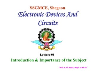
- 1. SSGMCE, Shegaon Electronic Devices And Circuits Lecture 01 Introduction & Importance of the Subject Prof. A. N. Dolas, Dept. of E&TC
- 2. Introduction • Why the name ‘electronics’? I mean why not protonics or neutronics? Prof. A. N. Dolas, Dept. of E&TC
- 3. Introduction Contd. • What is electronics? The IRE has defined electronics in proceedings of IRE vol.38(1950) as that: “ The Field of Science & Engineering, which deals with the study, design and use of devices, which depends on the conduction of electricity through a vacuum, gas or semiconductor”. Prof. A. N. Dolas, Dept. of E&TC
- 4. Beginning and Development of Electronics • 1850- German scientist Geissler If the air is removed from a glass tube, it glows when an electric current passes through it. • 1878- British scientist, Sir William Crookes The current in vacuum tubes seemed to consist of particles. Prof. A. N. Dolas, Dept. of E&TC
- 5. Beginning and Development of Electronics Contd.. • 1897- Electron is discovered • French physicist, Perrin demonstrated that current in a vacuum tube consists of the movement of negatively charged particles in a given direction. Some of the properties of these particles were measured by British physicist Thomson. • These negatively charged particles were later on, named as electrons Prof. A. N. Dolas, Dept. of E&TC
- 6. Beginning and Development of Electronics Contd.. • 1909- An American physicist Measured the charge on an electron. Result of these discoveries, the movement of electron could be controlled, and thus the electron era started. Prof. A. N. Dolas, Dept. of E&TC
- 7. Beginning and Development of Electronics Contd.. • 1904-Fleming(Fleming Tube or diode vacuum tube) Invented a vacuum tube that allowed electrical current only in one direction. • 1907- An American Scientist Lee deForest Invented a tube, which could amplify weak electrical signals. Named as Triode vacuum tube. Prof. A. N. Dolas, Dept. of E&TC
- 8. Beginning and Development of Electronics Contd.. • Around 1915- Triode vacuum tube used in oscillator circuit and telephone system. • 1916-Tetrode invented by a German engineer. • 1926- Pentode invented by a Dutch engineer. Prof. A. N. Dolas, Dept. of E&TC
- 9. Beginning and Development of Electronics Contd.. • 1920- Invented first TV picture tube, called the Kinescope, by an American researcher. • Several types of microwave tubes were invented during world War II. Prof. A. N. Dolas, Dept. of E&TC
- 10. Beginning and Development of Electronics Contd.. • 1947- Walter Britain, John Bardeen and William Shockley Invented transistor at Bell laboratory (America). Produced commercially in 1951. • 1959-Robert Noyce given an idea for making multiple devices on a single piece of silicon. Prof. A. N. Dolas, Dept. of E&TC
- 11. Functions • Rectification (DC Generation) • Amplification • Control • Generation (Oscillators) • Conversion of light into electricity • Conversion of electricity into light Prof. A. N. Dolas, Dept. of E&TC
- 12. Syllabus • Diode • Transistor • Transistorized circuits • Special purpose diodes • FET, UJT Prof. A. N. Dolas, Dept. of E&TC
- 13. Importance of Subject • Basic subject in Electronics engineering. • Subject plays vital role to understand electronics and communication. • Thorough understanding of this subject will provide the strong platform to the student for study of higher-level electronics. Prof. A. N. Dolas, Dept. of E&TC
- 14. SNo. Title Author Publication T-1 Electronics Devices & Circuits Jacob Milman and Christos C. Halkies Tata McGraw Hill Book Co., New Delhi. T-2 Electronics Devices & Circuits Allen Mottershead Prentice Hall of India Private Limited, New Delhi. T-3 Electronics Devices & Circuits Boylestad R. Prentice Hall of India Private Limited, New Delhi. T-4 Applied Electronics R.S. Sedha S-chand Publications, NewDelhi. Prof. A. N. Dolas, Dept. of E&TC
- 15. SNo. Title Author Publication R-1 Basic Electronics Bernard Grob Tata Mc-Graw Hill Publishing Company, New Delhi. R-2 Basic Electronics Solid State B. L. Thereja R-3 Microelectronic Circuits Theory and Applications Adel S. Sedra Kenneth C. Smith Oxford university press Prof. A. N. Dolas, Dept. of E&TC
- 16. Basic Electronics Things to be covered: • What is electricity • Voltage, Current, Resistance • Ohm’s Law • Capacitors, Inductors • Semiconductors • Mechanical Components • Digital Electronics Prof. A. N. Dolas, Dept. of E&TC
- 17. What is Electricity • Everything is made of atoms • There are 118 elements, an atom is a single part of an element • Atom consists of electrons, protons, and neutrons Prof. A. N. Dolas, Dept. of E&TC
- 18. • Electrons (- charge) are attracted to protons (+ charge), this holds the atom together • Some materials have strong attraction and refuse to loss electrons, these are called insulators (air, glass, rubber, most plastics) • Some materials have weak attractions and allow electrons to be lost, these are called conductors (copper, silver, gold, aluminum) • Electrons can be made to move from one atom to another, this is called a current of electricity. Prof. A. N. Dolas, Dept. of E&TC
- 19. • Surplus of electrons is called a negative charge (-). A shortage of electrons is called a positive charge (+). • A battery provides a surplus of electrons by chemical reaction. • By connecting a conductor from the positive terminal to negative terminal electrons will flow. Prof. A. N. Dolas, Dept. of E&TC
- 20. Voltage • A battery positive terminal (+) and a negative terminal (-). The difference in charge between each terminal is the potential energy the battery can provide. This is labeled in units of volts. Water Analogy Prof. A. N. Dolas, Dept. of E&TC
- 21. Voltage Sources: Prof. A. N. Dolas, Dept. of E&TC
- 22. • Voltage is like differential pressure, always measure between two points. • Measure voltage between two points or across a component in a circuit. • When measuring DC voltage make sure polarity of meter is correct, positive (+) red, negative (-) black. Prof. A. N. Dolas, Dept. of E&TC
- 23. Ground Prof. A. N. Dolas, Dept. of E&TC
- 24. Exercise • Measure DC voltage from power supply using multimeter • Measure DC voltage from power supply using oscilloscope • Measure DC voltage from battery using multimeter • Measure AC voltage from wall outlet using a multimeter • Measure AC voltage from wall outlet using an oscilloscope Effective or Root Mean Square Voltage (Measured with multimeter) ERMS=0.707xEA E Prof. A. N. Dolas, Dept. of E&TC
- 25. Current • Uniform flow of electrons thru a circuit is called current. WILL USE CONVENTIONAL FLOW NOTATION ON ALL SCHEMATICS Prof. A. N. Dolas, Dept. of E&TC
- 26. • To measure current, must break circuit and install meter in line. • Measurement is imperfect because of voltage drop created by meter. Prof. A. N. Dolas, Dept. of E&TC
- 27. Resistance • All materials have a resistance that is dependent on cross- sectional area, material type and temperature. • A resistor dissipates power in the form of heat Prof. A. N. Dolas, Dept. of E&TC
- 28. Various resistors types Prof. A. N. Dolas, Dept. of E&TC
- 29. When measuring resistance, remove component from the circuit. Prof. A. N. Dolas, Dept. of E&TC
- 30. Resistor Color Code Prof. A. N. Dolas, Dept. of E&TC
- 31. • Determine the resistance of various resistors of unknown value using the resistor color code • Using the multimeter, compare the specified resistance and measured resistance • Using the multimeter to examine the characteristics of various potentiometers Exercise Prof. A. N. Dolas, Dept. of E&TC
- 32. Ohm’s Law Prof. A. N. Dolas, Dept. of E&TC
- 33. Prototyping Board Example of how components are Inserted in the protoboard Prof. A. N. Dolas, Dept. of E&TC
- 34. Exercise • Calculate the total current and voltage drop across each resistor shown in Figure 1 • Build the circuit in Figure 1 on the prototype board • Measure the total circuit current and voltage drops across each resistor and compare the calculated and measured values Prof. A. N. Dolas, Dept. of E&TC
- 35. Capacitance Battery Capacitor Unit = Farad Pico Farad - pF = 10-12F Micro Farad - uF = 10-6F A capacitor is used to store charge for a short amount of time Prof. A. N. Dolas, Dept. of E&TC
- 36. Prof. A. N. Dolas, Dept. of E&TC
- 37. Capacitor Charging Prof. A. N. Dolas, Dept. of E&TC
- 38. Capacitor Discharge Prof. A. N. Dolas, Dept. of E&TC
- 39. Inductance Prof. A. N. Dolas, Dept. of E&TC
- 40. Prof. A. N. Dolas, Dept. of E&TC
- 41. Discussion!! Prof. A. N. Dolas, Dept. of E&TC
- 42. SSGMCE, Shegaon Electronic Devices And Circuits Lecture 02 Atomic Structure Prof. A. N. Dolas, Dept. of E&TC
- 43. Electrons in Isolated Atoms • Isolated atoms have energy levels – The electrons can only be found in these energy states Prof. A. N. Dolas, Dept. of E&TC
- 44. Atoms in Solids • Atoms form a lattice structure The lattice affects the structure of the energy levels of each atom – we now have joint levels for the entire structure Prof. A. N. Dolas, Dept. of E&TC
- 45. Intrinsic Semiconductor • Elemental or pure semiconductors have equal numbers of holes and electrons – Depends on temperature, type, and size. • Compound Semiconductors can be formed from two (or more) elements (e.g., GaAs) Prof. A. N. Dolas, Dept. of E&TC
- 46. Extrinsic Semiconductors • A pure semiconductors where a small amount of another element is added to replace atoms in the lattice (doping). – The aim is to produce an excess of either electrons (n-type) or holes (p-type) – Typical doping concentrations are one part in ten million – Doping must be uniform throughout the lattice so that charges do not accumulate Prof. A. N. Dolas, Dept. of E&TC
- 47. N-Type and P-Type • One valence electron too many (n-type) – Arsenic, antimony, bismuth, phosphorus • One valence electron too few (p-type) – Aluminum, indium, gallium, boron Prof. A. N. Dolas, Dept. of E&TC
- 48. What Are Diodes Made Out Of? • Silicon (Si) and Germanium (Ge) are the two most common single elements that are used to make Diodes. A compound that is commonly used is Gallium Arsenide (GaAs), especially in the case of LEDs because of it’s large bandgap. • Silicon and Germanium are both group 4 elements, meaning they have 4 valence electrons. Their structure allows them to grow in a shape called the diamond lattice. • Gallium is a group 3 element while Arsenide is a group 5 element. When put together as a compound, GaAs creates a zincblend lattice structure. • In both the diamond lattice and zincblend lattice, each atom shares its valence electrons with its four closest neighbors. This sharing of electrons is what ultimately allows diodes to be build. When dopants from groups 3 or 5 (in most cases) are added to Si, Ge or GaAs it changes the properties of the material so we are able to make the P- and N-type materials that become the diode. Si +4 Si +4 Si +4 Si +4 Si +4 Si +4 Si +4 Si +4 Si +4 The diagram above shows the 2D structure of the Si crystal. The light green lines represent the electronic bonds made when the valence electrons are shared. Each Si atom shares one electron with each of its four closest neighbors so that its valence band will have a full 8 electrons. Prof. A. N. Dolas, Dept. of E&TC
- 49. N-Type Material N-Type Material: When extra valence electrons are introduced into a material such as silicon an n-type material is produced. The extra valence electrons are introduced by putting impurities or dopants into the silicon. The dopants used to create an n-type material are Group V elements. The most commonly used dopants from Group V are arsenic, antimony and phosphorus. The 2D diagram to the left shows the extra electron that will be present when a Group V dopant is introduced to a material such as silicon. This extra electron is very mobile. +4 +4 +5 +4 +4 +4 +4 +4 +4 Prof. A. N. Dolas, Dept. of E&TC
- 50. P-Type Material P-Type Material: P-type material is produced when the dopant that is introduced is from Group III. Group III elements have only 3 valence electrons and therefore there is an electron missing. This creates a hole (h+), or a positive charge that can move around in the material. Commonly used Group III dopants are aluminum, boron, and gallium. The 2D diagram to the left shows the hole that will be present when a Group III dopant is introduced to a material such as silicon. This hole is quite mobile in the same way the extra electron is mobile in a n-type material. +4 +4 +3 +4 +4 +4 +4 +4 +4 Prof. A. N. Dolas, Dept. of E&TC
- 51. Discussion!! Prof. A. N. Dolas, Dept. of E&TC
- 52. SSGMCE, Shegaon Electronic Devices And Circuits Lecture 03 & 04 Semiconductor Diode Prof. A. N. Dolas, Dept. of E&TC
- 53. The PN Junction Steady State1 P n - - - - - - - - - - - - - - - - - - - - - - - - - - - - - - + + + + + + + + + + + + + + + + + + + + + + + + + + + + + + Na Nd Metallurgical Junction Space Charge Region ionized acceptors ionized donors E-Field + + _ _ h+ drift h+ diffusion e- diffusion e- drift = = Prof. A. N. Dolas, Dept. of E&TC
- 54. The PN Junction Steady State P n - - - - - - - - - - - - - - - - - - - - + + + + + + + + + + + + + + + + + + + + Na Nd Metallurgical Junction Space Charge Region ionized acceptors ionized donors E-Field + + _ _ h+ drift h+ diffusion e- diffusion e- drift = = = = When no external source is connected to the pn junction, diffusion and drift balance each other out for both the holes and electrons Space Charge Region: Also called the depletion region. This region includes the net positively and negatively charged regions. The space charge region does not have any free carriers. The width of the space charge region is denoted by W in pn junction formula’s. Metallurgical Junction: The interface where the p- and n-type materials meet. Na & Nd: Represent the amount of negative and positive doping in number of carriers per centimeter cubed. Usually in the range of 1015 to 1020. Prof. A. N. Dolas, Dept. of E&TC
- 55. The Biased PN Junction P n + _ Applied Electric Field Metal Contact “Ohmic Contact” (Rs~0) + _ Vapplied I The pn junction is considered biased when an external voltage is applied. There are two types of biasing: Forward bias and Reverse bias. These are described on then next slide. Prof. A. N. Dolas, Dept. of E&TC
- 56. The Biased PN Junction Forward Bias: In forward bias the depletion region shrinks slightly in width. With this shrinking the energy required for charge carriers to cross the depletion region decreases exponentially. Therefore, as the applied voltage increases, current starts to flow across the junction. The barrier potential of the diode is the voltage at which appreciable current starts to flow through the diode. The barrier potential varies for different materials. Reverse Bias: Under reverse bias the depletion region widens. This causes the electric field produced by the ions to cancel out the applied reverse bias voltage. A small leakage current, Is (saturation current) flows under reverse bias conditions. This saturation current is made up of electron-hole pairs being produced in the depletion region. Saturation current is sometimes referred to as scale current because of it’s relationship to junction temperature. Vapplied > 0 Vapplied < 0 Prof. A. N. Dolas, Dept. of E&TC
- 57. Properties of Diodes Figure 1.10 – The Diode Transconductance Curve2 • VD = Bias Voltage • ID = Current through Diode. ID is Negative for Reverse Bias and Positive for Forward Bias • IS = Saturation Current • VBR = Breakdown Voltage • V = Barrier Potential Voltage VD ID (mA) (nA) VBR ~V IS Prof. A. N. Dolas, Dept. of E&TC
- 58. Discussion!! Prof. A. N. Dolas, Dept. of E&TC
- 59. SSGMCE, Shegaon Electronic Devices And Circuits Lecture 05 Energy Band Structure Prof. A. N. Dolas, Dept. of E&TC
- 60. Band Theory • Three bands of energy levels form – Valence Band – most of the electrons are here – Conduction Band – electrons here give the material electrical conductivity – Forbidden Band – electrons must jump this band to get from the valence to the conduction band Prof. A. N. Dolas, Dept. of E&TC
- 61. Lattice Bands Prof. A. N. Dolas, Dept. of E&TC
- 62. Properties of Diodes The Shockley Equation • The transconductance curve on the previous slide is characterized by the following equation: ID = IS(eVD/VT – 1) • As described in the last slide, ID is the current through the diode, IS is the saturation current and VD is the applied biasing voltage. • VT is the thermal equivalent voltage and is approximately 26 mV at room temperature. The equation to find VT at various temperatures is: VT = kT q k = 1.38 x 10⁻²³ J/K T = temperature in Kelvin q = 1.6 x 10⁻¹⁹ C • is the emission coefficient for the diode. It is determined by the way the diode is constructed. It somewhat varies with diode current. For a silicon diode is around 2 for low currents and goes down to about 1 at higher currents Prof. A. N. Dolas, Dept. of E&TC
- 63. Resistivity R T Conductor Semiconductor Prof. A. N. Dolas, Dept. of E&TC
- 64. Conduction • In order for an electron to become free and participate in current flow, it must gain enough energy to jump over the forbidden band • For semiconductors at room temperature, there is not enough energy to conduct. • As temperature increases more electrons have the energy to jump the forbidden band – Resistivity decreases – This is the opposite behavior of conductors Prof. A. N. Dolas, Dept. of E&TC
- 65. Semiconductors • When an electron becomes free, it creates a “hole” in the lattice structure A hole is effectively a positive charge Prof. A. N. Dolas, Dept. of E&TC
- 66. Electron and Hole Movement Prof. A. N. Dolas, Dept. of E&TC
- 67. Discussion!! Prof. A. N. Dolas, Dept. of E&TC
- 68. SSGMCE, Shegaon Electronic Devices And Circuits Lecture 06 Biasing Diode Prof. A. N. Dolas, Dept. of E&TC
- 69. In a dc circuit Prof. A. N. Dolas, Dept. of E&TC
- 70. The PN Junction Diode Start with a P and N type material. Note that there is excess negatives in the n-type and excess positives in the p-type Merge the two – some of the negatives migrate over to the p-type, filling in the holes. The yellow region is called the depletion zone. More positive than rest of N More negative than rest of P Prof. A. N. Dolas, Dept. of E&TC
- 71. Biasing the Junction Apply a voltage as indicated. The free charge carriers (negative charges in the N material and positive charges in the P material) are attracted to the ends of the crystal. No charge flows across the junction and the depletion zone grows. This is called reverse bias. Switch polarity. Now the negative charges are driven toward the junction in the N material and the positive charges also are driven toward the junction in the P material. The depletion zone shrinks and will disappear if the voltage exceeds a threshold. This is called forward bias. Prof. A. N. Dolas, Dept. of E&TC
- 72. Diode Circuit Symbols Reverse Bias Forward Bias N material (cathode) P material (anode) Prof. A. N. Dolas, Dept. of E&TC
- 73. I-V Curve Recall Ohm’s Law (V=IR) Put it into slope-intercept form to get I = V/R. The slope of the graph is 1/R. Large slopes mean small R. Prof. A. N. Dolas, Dept. of E&TC
- 74. Types of Diodes • Rectifier Diode – Used in power supplies • Signal Diode – Used in switches, detectors, mixers, etc. • Zener Diode – Voltage regulation – operated reverse bias in the avalanche region • Reference Diode – Used like zener for voltage regulation Prof. A. N. Dolas, Dept. of E&TC
- 75. Types of Diodes • Varactor Diode – PN junction exhibits capacitive properties • Depletion zone acts like a dielectric • Adjacent material acts like the capacitor plates – Increasing reverse bias decreases capacitance – recall – Capacitance Effect is destroyed if the forward bias is great enough to destroy the depletion zone d A C o Prof. A. N. Dolas, Dept. of E&TC
- 76. Discussion!! Prof. A. N. Dolas, Dept. of E&TC
- 77. SSGMCE, Shegaon Electronic Devices And Circuits Lecture 08 Zener Diode Prof. A. N. Dolas, Dept. of E&TC
- 78. Precise Voltage Regulation • If the load current is varying, but you require voltage to be constant, R must vary (V=IR). Prof. A. N. Dolas, Dept. of E&TC
- 79. The Avalanche Region • Increasing reverse bias on the diode eventually accelerates electrons in the depletion zone so that they ionize other atoms. – The freed electrons ionize other atoms – Avalanche occurs • Zener Diodes are designed so that the transition potential is very steep Prof. A. N. Dolas, Dept. of E&TC
- 80. Zener I-V Curve For a large change of current, voltage remains at VZ Zener acts like an automatically varying resistor. Can be obtained with VZ from 2.4 – 200 V. Prof. A. N. Dolas, Dept. of E&TC
- 81. Zener Regulation Circuit Since the load is in parallel with the diode, the voltage drop across RL is always the same as across VR1 and is VZ = constant Zener voltage The input voltage V must be greater than VZ. Zener MUST be operated under load. If not, the zener is still delivering power (more than usual) and may melt. Recall that the zener can draw large currents all at the same voltage. Prof. A. N. Dolas, Dept. of E&TC
- 82. Discussion!! Prof. A. N. Dolas, Dept. of E&TC
- 83. SSGMCE, Shegaon Electronic Devices And Circuits Lecture 10 Half Wave Rectifier Prof. A. N. Dolas, Dept. of E&TC
- 84. Rectification • Conversion of ac to dc. – Many devices (transistors) are unidirectional current devices – DC required for proper operation. Prof. A. N. Dolas, Dept. of E&TC
- 85. Half Wave Rectifier Prof. A. N. Dolas, Dept. of E&TC
- 86. Discussion!! Prof. A. N. Dolas, Dept. of E&TC
- 87. SSGMCE, Shegaon Electronic Devices And Circuits Lecture 11 Full Wave Rectifier & Filters Prof. A. N. Dolas, Dept. of E&TC
- 88. Full Wave Rectifier Prof. A. N. Dolas, Dept. of E&TC
- 89. Full Wave Rectifier Prof. A. N. Dolas, Dept. of E&TC
- 90. Bridge Rectifier Prof. A. N. Dolas, Dept. of E&TC
- 91. Bridge Rectifier Prof. A. N. Dolas, Dept. of E&TC
- 92. Filters • We have now used diodes to produced a pulsed dc signal. • Most equipment requires “regulated” dc – We must remove the “ripple” – Ripple is departure of waveform from pure dc (flat, constant voltage level) • Frequency – so far we have seen pulsed dc at the same frequency as the input (½ wave) or twice the line frequency (full wave rectifier) • Amplitude – a measure of the effectiveness of the filter Prof. A. N. Dolas, Dept. of E&TC
- 93. Ripple Factor out) V(average out) voltage ripple ( V r rms Low r indicates better filtering Prof. A. N. Dolas, Dept. of E&TC
- 94. Alternate Definition • Defined also for current – Iac = effective value of ac harmonic component – Idc = average of dc component 2 dc 2 rms ac 2 ac 2 dc rms I I I so, I I I 1 I I r I I r 2 dc rms dc ac For ½-wave rectifier r = 1.21 For full-wave rectifier r = 0.48 Prof. A. N. Dolas, Dept. of E&TC
- 95. High Pass (RC) Filter 2 2 2 C 2 C f 2 1 R X R Z 2 2 i i C f 2 1 R V Z V I Prof. A. N. Dolas, Dept. of E&TC
- 96. High Pass Filter • I is the same through both R and C 2 i o 2 2 i o RC f 2 1 1 1 V V C f 2 1 R RV RI V When f is small, denominator is large and the voltage ratio is small. When f is large, denominator is almost one Prof. A. N. Dolas, Dept. of E&TC
- 97. Typical Results R = 0.1 MW C = 0.16 mF Why is it called a high pass filter? Prof. A. N. Dolas, Dept. of E&TC
- 98. Half Power Point • Note the point at which – This will make (Vo/Vi )2 = ½ – Recall that one form of power is V2/R, so the output power is half the input power at this frequency. 2 1 V V i o Prof. A. N. Dolas, Dept. of E&TC
- 99. Low Pass (RC) Filter Z V I i C I IX IZ V C C o 2 2 2 C 2 C 1 R X R Z Prof. A. N. Dolas, Dept. of E&TC
- 100. Low Pass Filter 2 i o 2 i o 2 2 i o C R 1 1 V V 1 C R V V C 1 R C V C I V Low frequency means denominator is small and Vo / Vi 1 High frequency means denominator is large and Vo / Vi is small Prof. A. N. Dolas, Dept. of E&TC
- 101. Low Pass Results Note the half power frequency again. Prof. A. N. Dolas, Dept. of E&TC
- 102. Half Wave Capacitive Filter • Improving the ripple factor – During forward bias half-cycle, capacitor is charging – During the reverse bias half-cycle, the capacitor discharges through the output resistor Prof. A. N. Dolas, Dept. of E&TC
- 103. Full Wave Capacitive Filter • Even better ripple factor. Prof. A. N. Dolas, Dept. of E&TC
- 104. L-Section Filter • The series inductor opposes changes in current • The coil stores energy when the current is above average and releases energy to the circuit when the current falls below average Coil chops off (chokes) the peaks of the ac pulses L-section delivers more steady current than the capacitive filter alone Used for cases of variable loads where good regulation is required Output voltage is less than the capacitive filter Prof. A. N. Dolas, Dept. of E&TC
- 105. P Filter Combines the effects of a capacitive and L-section filter. Regulation is poor when load varies, however. Prof. A. N. Dolas, Dept. of E&TC
- 106. Discussion!! Prof. A. N. Dolas, Dept. of E&TC