Download as PDF, PPTX


![16 COOLCHIPS 21 | AMD EPYCTM MICROPROCESSOR ARCHITECTURE
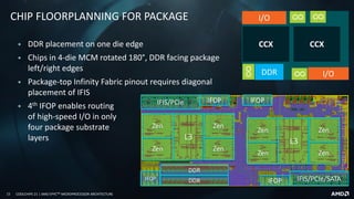
ADVANCED PACKAGING
▪ 58mm x 75mm organic package
▪ 4 die-to-die IFOP links/die
‒ 3 connected/die
▪ 2 SERDES/die to pins
‒ 1/die to “top” (G) and “bottom” (P) links
‒ Balanced I/O for 1P, 2P systems
▪ 2 DRAM-channels/die to pins
Purpose-built MCM Architecture
G[0-3], P[0-3] : 16 lane high-speed SERDES Links
M[A-H] : 8 x72b DRAM channels
: Die-to-Die Infinity Fabric On-Package links
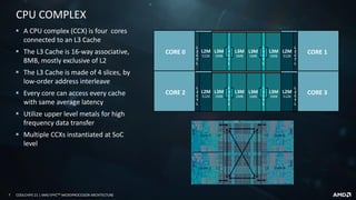
CCX: 4Core + L2/core + shared L3 complex
P1
P0
P2
P3
G2
G3
G1
G0
MF
MG
MH
ME
Die-to-Package Topology Mapping
MA
MD
MC
MB
I/ODDR
CCX
CCX
Die 1
I/O
I/ODDR
CCX
CCX
Die 3
I/O
I/ODDR
CCX
CCX
Die 2
I/O
I/ODDR
CCX
CCX
Die 0
I/O](https://image.slidesharecdn.com/coolchips20180418finalpresentationforexternaldistribution-180423154800/85/AMD-EPYC-Microprocessor-Architecture-16-320.jpg)


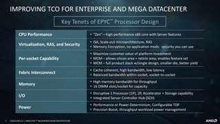
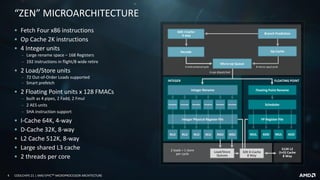
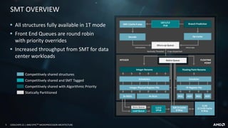
This document provides an overview of the AMD EPYCTM microprocessor architecture. It discusses the key tenets of the EPYC processor design including the "Zen" CPU core, virtualization and security features, high per-socket capability through its multi-chip module (MCM) design, high bandwidth fabric interconnect, large memory capacity and disruptive I/O capabilities. It also details the microarchitecture of the "Zen" core and how it was designed and optimized for data center workloads.