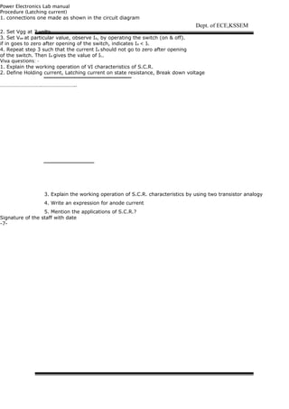
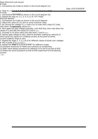
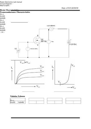
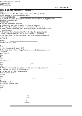
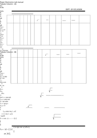
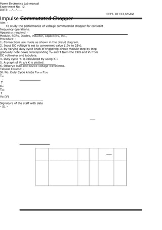
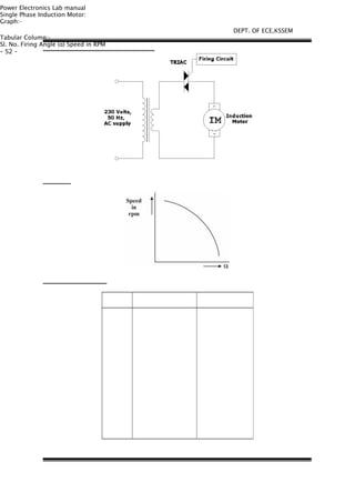
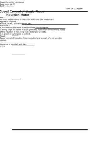
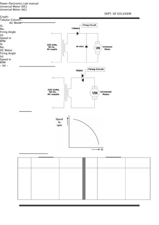
Download to read offline


![Power Electronics Lab manual
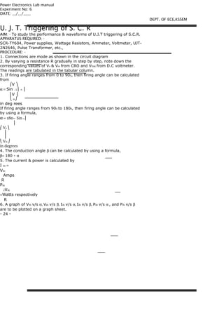
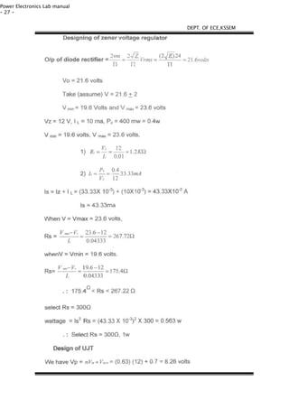
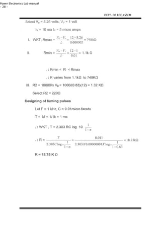
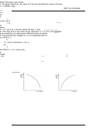
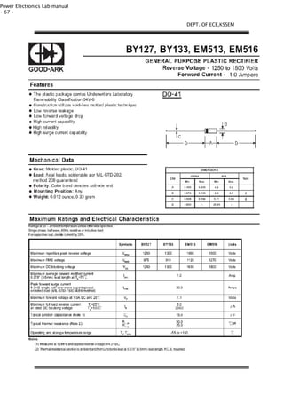
7. For given frequency, the value of R can be calculated by using a formula,
T = 2.303RC. log10
R=
T
1
1−η
Ω
1
C2.303 .log10
1 −η
When
C = 0.1 mF & N = Intrinsic stand off ratio = 0.67
8. This value of R is set in the circuit, Step No S 3. 4. 5. & 6. are repeated
and waveforms are observed at different points as shown.
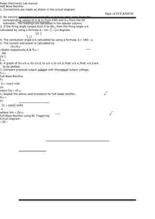
9. Compare Voth with VoPractical where Voth =
Vm
[1 + cos α]
π
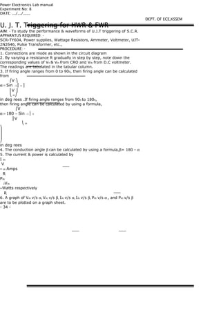
VIVA QUESTIONS: -
1. Explain the working operation of U.J.T. triggering circuit waveforms?
2. Why U.J.T. Triggering circuit is superior when compared to R & RC
triggering circuit?
3. What is the use of pulse transformer?
4. Explain the design part of UJT?
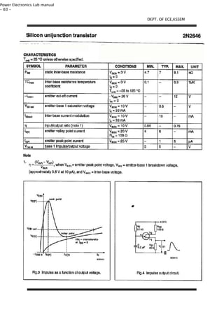
5. Write equivalent circuit of UJT and show that Vpeak = Vemitter = Vγ+ηVBB.
6. Why do we require turn-on circuits for thyristors?
7. Why do we require turn-off circuits for thyristors?
8. Comment on Forced & Natural Commutation techniques.
………………………………………………….
Signature of the staff-in-charge
- 26 -
DEPT. OF ECE,KSSEM](https://image.slidesharecdn.com/pelabconverted-141222085454-conversion-gate01/85/Pe-lab-converted-27-320.jpg)
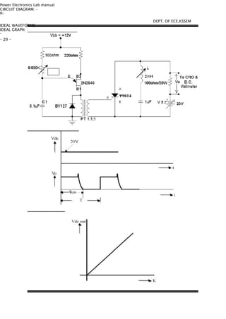


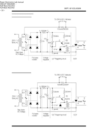
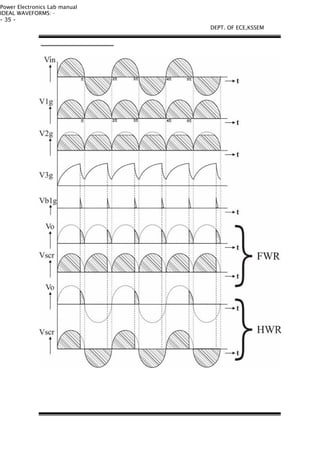
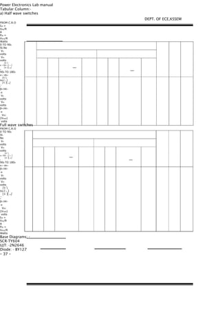


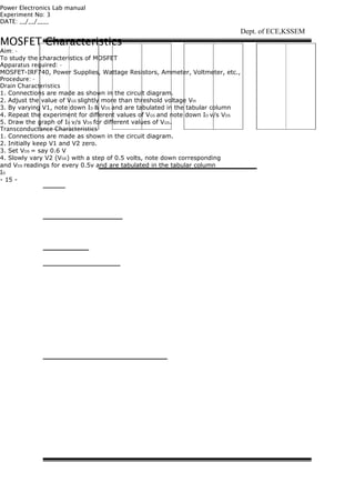
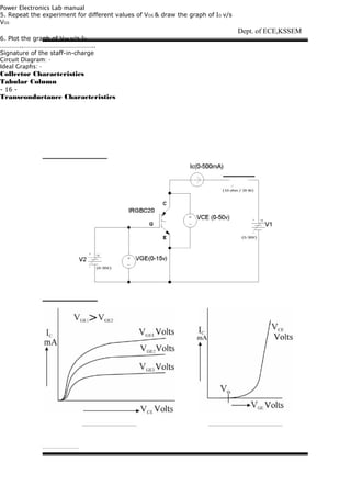
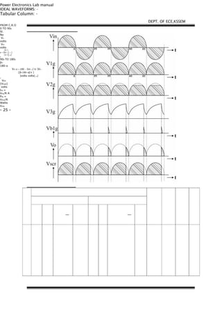
1. The document describes experiments to study the characteristics of various power electronics devices like SCR, TRIAC, MOSFET, IGBT using different circuit connections and varying parameters. 2. Procedures to study half wave and full wave rectification using RC triggering circuit are provided along with the relevant circuit diagram and waveforms. Readings are noted in a tabular column and graphs are plotted. 3. Signatures of staff conducting the experiments are included indicating the experiments were performed in the power electronics lab.


