8 Channel Bi Directional Logic Level Converter
•
0 likes•685 views

Because the Arduino (and Basic Stamp) are 5V devices, and most modern sensors, displays, flash cards and modes are 3.3V-only, many makers find that they need to perform level shifting/conversion to protect the 3.3V device from 5V.This 8-bit non inverting translator uses two separate configurable power-supply rails. The A port is designed to track VCCA. VCCA accepts any supply voltage from 1.2 V to 3.6 V. The B port is designed to track VCCB. VCCB accepts any supply voltage from 1.65 V to 5.5 V. This allows for universal low-voltage bidirectional translation between any of the 1.2-V, 1.5-V, 1.8-V, 2.5-V, 3.3-V, and 5-V voltage nodes. VCCA should not exceed VCCB.

Recommended
Recommended
More Related Content
What's hot
What's hot (20)
Viewers also liked
Viewers also liked (16)
Similar to 8 Channel Bi Directional Logic Level Converter
Similar to 8 Channel Bi Directional Logic Level Converter (20)
More from Raghav Shetty
More from Raghav Shetty (20)
Recently uploaded
Recently uploaded (20)
8 Channel Bi Directional Logic Level Converter
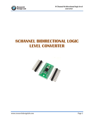
- 1. www.researchdesignlab.com Page 1 8 Channel bi-directional logic level converter 8CHANNEL BIDIRECTIONAL LOGIC LEVEL CONVERTER
- 2. www.researchdesignlab.com Page 2 8 Channel bi-directional logic level converter Table of Contents OVERVIEW ................................................................................................................................... 3 INTRODUCTION ...................................................................................................................... 3 FEATURES ................................................................................................................................ 3 APPLICATIONS........................................................................................................................ 4 TXB0108IC................................................................................................................................. 4 PIN DESCRIPTION ................................................................................................................... 5 RELATED PRODUCTS ............................................................................................................ 8
- 3. www.researchdesignlab.com Page 3 8 Channel bi-directional logic level converter OVERVIEW INTRODUCTION Because the Arduino (and Basic Stamp) are 5V devices, and most modern sensors, displays, flash cards and modes are 3.3V-only, many makers find that they need to perform level shifting/conversion to protect the 3.3V device from 5V.This 8-bit non inverting translator uses two separate configurable power-supply rails. The A port is designed to track VCCA. VCCA accepts any supply voltage from 1.2 V to 3.6 V. The B port is designed to track VCCB. VCCB accepts any supply voltage from 1.65 V to 5.5 V. This allows for universal low-voltage bidirectional translation between any of the 1.2-V, 1.5-V, 1.8-V, 2.5-V, 3.3-V, and 5-V voltage nodes. VCCA should not exceed VCCB. FEATURES 1.2 V to 3.6 V on A Port and 1.65 to 5.5 V on B Port (VCCA ≤ VCCB). VCC Isolation Feature – If Either VCC Input Is at GND, All Outputs Are in the High- Impedance State. OE Input Circuit Referenced to VCCA. Low Power Consumption, 4-mA Max ICC. Ioff Supports Partial-Power-Down Mode Operation. High quality PCB FR4 Grade with FPT Certified.
- 4. www.researchdesignlab.com Page 4 8 Channel bi-directional logic level converter APPLICATIONS Handset Smartphone Tablet Desktop PC TXB0108IC
- 5. www.researchdesignlab.com Page 5 8 Channel bi-directional logic level converter CIRCUIT DIAGRAM PIN DESCRIPTION
- 6. www.researchdesignlab.com Page 6 8 Channel bi-directional logic level converter NAME FUNCTION A1 Input/output 1. Referenced to VCCA VCCA A-port supply voltage. 1.1 V ≤ VCCA ≤ 3.6 V, VCCA ≤ VCCB. A2 Input/output 2. Referenced to VCCA. A3 Input/output 3. Referenced to VCCA. A4 Input/output 4. Referenced to VCCA. A5 Input/output 5. Referenced to VCCA. A6 Input/output 6. Referenced to VCCA. A7 Input/output 7. Referenced to VCCA. A8 Input/output 8. Referenced to VCCA. OE Output enable. Pull OE low to place all outputs in 3-state mode. Referenced to VCCA. GND Ground B8 Input/output 8. Referenced to VCCB. B7 Input/output 7. Referenced to VCCB. B6 Referenced to VCCB. B5 Input/output 5. Referenced to VCCB.
- 7. www.researchdesignlab.com Page 7 8 Channel bi-directional logic level converter B4 Input/output 4. Referenced to VCCB. B3 Input/output 3. Referenced to VCCB. B2 Input/output 2. Referenced to VCCB. VCCB B-port supply voltage. 1.65 V ≤ VCCB ≤ 5.5V. B1 Input/output 1. Referenced to VCCB. NOTE: TXB0108 should not be used in applications such as I2C or 1-wire where an open drain driver is connected on the Bi-directional data I/O
- 8. www.researchdesignlab.com Page 8 8 Channel bi-directional logic level converter RELATED PRODUCTS DIY UNO Play Breadboard -ATMEGA328P Expansion Board Compatible for Raspberry Pi RDL- UNO ATMEGA328 Development Board 3 in 1(= Uno+Memory Shield+Xbee Shield) - Programmed with Arduino