Download to read offline


![NOTES
1
VA and VB represent the Mean Average Deviation (MAD) of the detected sine waves. Note that for this Transfer Function to linearly represent positive displacement,
the sum of VA and VB of the LVDT must remain constant with stroke length. See “Theory of Operation.” Also see Figures 7 and 12 for R2.
2
From TMIN, to TMAX, the overall error due to the AD598 alone is determined by combining gain error, gain drift and offset drift. For example the worst case overall
error for the AD598AD from TMIN to TMAX is calculated as follows: overall error = gain error at +25°C (±1% full scale) + gain drift from –40°C to +25°C (50 ppm/°C
of FS × +65°C) + offset drift from –40°C to +25°C (50 ppm/°C of FS × +65°C) = ±1.65% of full scale. Note that 1000 ppm of full scale equals 0.1% of full scale.
Full scale is defined as the voltage difference between the maximum positive and maximum negative output.
3
Nonlinearity of the AD598 only, in units of ppm of full scale. Nonlinearity is defined as the maximum measured deviation of the AD598 output voltage from a
straight line. The straight line is determined by connecting the maximum produced full-scale negative voltage with the maximum produced full-scale positive voltage.
4
See Transfer Function.
5
This offset refers to the (VA–VB)/(VA+VB) input spanning a full-scale range of ±1. [For (VA–VB)/(VA+VB) to equal +1, VB must equal zero volts; and correspondingly
for (VA–VB)/(VA+VB) to equal –1, VA must equal zero volts. Note that offset errors do not allow accurate use of zero magnitude inputs, practical inputs are limited to
100 mV rms.] The ±1 span is a convenient reference point to define offset referred to input. For example, with this input span a value of R2 = 20 k Ω would give
VOUT span a value of ±10 volts. Caution, most LVDTs will typically exercise less of the ((VA–VB))/((VA+VB)) input span and thus require a larger value of R2 to
produce the ±10 V output span. In this case the offset is correspondingly magnified when referred to the output voltage. For example, a Schaevitz E100 LVDT
requires 80.2 kΩ for R2 to produce a ±10.69 V output and (VA–VB)/(VA+VB) equals 0.27. This ratio may be determined from the graph shown in Figure 18,
(VA–VB)/(VA+VB) = (1.71 V rms – 0.99 V rms)/(1.71 V rms + 0.99 V rms). The maximum offset value referred to the ±10.69 V output may be determined by
multiplying the maximum value shown in the data sheet (±1% of FS by 1/0.27 which equals ±3.7% maximum. Similarly, to determine the maximum values of offset
drift, offset CMRR and offset PSRR when referred to the ±10.69 V output, these data sheet values should also be multiplied by (1/0.27). For this example for the
AD598AD the maximum values of offset drift, PSRR offset and CMRR offset would be: 185 ppm/°C of FS; 741 ppm/V and 741 ppm/V respectively when referred
to the ±10.69 V output.
6
For example, if the excitation to the primary changes by 1 dB, the gain of the system will change by typically 100 ppm.
7
Output ripple is a function of the AD598 bandwidth determined by C2, C3 and C4. See Figures 16 and 17.
8
R1 is shown in Figures 7 and 12.
9
Excitation voltage drift is not an important specification because of the ratiometric operation of the AD598.
Specifications subject to change without notice.
Specifications shown in boldface are tested on all production units at final electrical test. Results from those tested are used to calculate outgoing quality levels. All
min and max specifications are guaranteed, although only those shown in boldface are tested on all production units.
AD598
THERMAL CHARACTERISTICS
θJC θJA
SOIC Package 22°C/W 80°C/W
Side Brazed Package 25°C/W 85°C/W
ABSOLUTE MAXIMUM RATINGS
Total Supply Voltage +VS to –VS . . . . . . . . . . . . . . . . . +36 V
Storage Temperature Range
R Package . . . . . . . . . . . . . . . . . . . . . . . . .–65°C to +150°C
D Package . . . . . . . . . . . . . . . . . . . . . . . . .–65°C to +150°C
Operating Temperature Range
AD598JR . . . . . . . . . . . . . . . . . . . . . . . . . . . . 0°C to +70°C
AD598AD . . . . . . . . . . . . . . . . . . . . . . . . . .–40°C to +85°C
Lead Temperature Range (Soldering 60 sec) . . . . . . . . +300°C
Power Dissipation Up to +65°C . . . . . . . . . . . . . . . . . . .1.2 W
Derates Above +65°C . . . . . . . . . . . . . . . . . . . . . . . 12 mW/°C
ORDERING GUIDE
Temperature Package Package
Model Range Description Option
AD598JR 0°C to +70°C SOIC R-20
AD598AD –40°C to +85C Ceramic DIP D-20
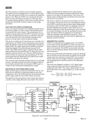
OFFSET 1
OFFSET 2
SIGNAL REFERENCE
SIGNAL OUTPUT
FEEDBACK
OUTPUT FILTER
A1 FILTER
A2 FILTER
EXC 1
EXC 2
LEVEL 1
LEVEL 2
FREQ 1
FREQ 2
B1 FILTER
B2 FILTER
1
2
3
4
5
6
7
8
9
10 11
12
13
14
16
15
17
18
19
20–VS +VS
AD598
TOP VIEW
(Not to Scale)
VB VA
REV. A –3–](https://image.slidesharecdn.com/ad598-170226204515/85/Ad598-4-320.jpg)
![AD598
REV. A –5–
a voltage proportional to position. This technique uses the pri-
mary excitation voltage as a phase reference to determine the
polarity of the output voltage. There are a number of problems
associated with this technique such as (1) producing a constant
amplitude, constant frequency excitation signal, (2) compensating
for LVDT primary to secondary phase shifts, and (3) compen-
sating for these shifts as a function of temperature and frequency.
The AD598 eliminates all of these problems. The AD598 does
not require a constant amplitude because it works on the ratio of
the difference and sum of the LVDT output signals. A constant
frequency signal is not necessary because the inputs are rectified
and only the sine wave carrier magnitude is processed. There is
no sensitivity to phase shift between the primary excitation and
the LVDT outputs because synchronous detection is not em-
ployed. The ratiometric principle upon which the AD598 oper-
ates requires that the sum of the LVDT secondary voltages
remains constant with LVDT stroke length. Although LVDT
manufacturers generally do not specify the relationship between
VA+VB and stroke length, it is recognized that some LVDTs do
not meet this requirement. In these cases a nonlinearity will
result. However, the majority of available LVDTs do in fact
meet these requirements.
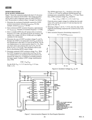
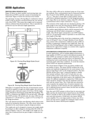
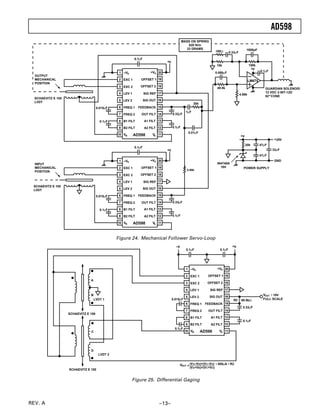
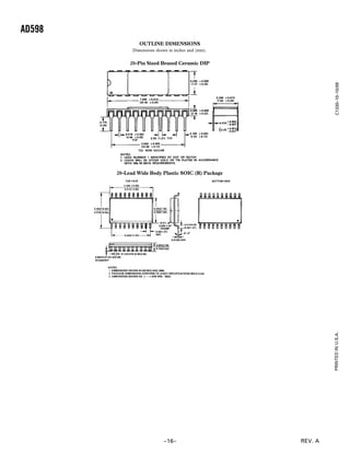
The AD598 utilizes a special decoder circuit. Referring to the
block diagram and Figure 6 below, an implicit analog comput-
ing loop is employed. After rectification, the A and B signals are
multiplied by complementary duty cycle signals, d and (I–d)
respectively. The difference of these processed signals is inte-
grated and sampled by a comparator. It is the output of this
comparator that defines the original duty cycle, d, which is fed
back to the multipliers.
As shown in Figure 6, the input to the integrator is [(A+B)d]B.
Since the integrator input is forced to 0, the duty cycle d =
B/(A+B).
The output comparator which produces d = B/(A+B) also con-
trols an output amplifier driven by a reference current. Duty
cycle signals d and (1–d) perform separate modulations on the
reference current as shown in Figure 6, which are summed. The
summed current, which is the output current, is IREF × (1–2d).
Since d = B/(A+B), by substitution the output current equals
IREF × (A–B)/(A+B). This output current is then filtered and
converted to a voltage since it is forced to flow through the scal-
ing resistor R2 such that:
VOUT = IREF ×( A – B) / (A + B)× R2
CONNECTING THE AD598
The AD598 can easily be connected for dual or single supply
operation as shown in Figures 7 and 12. The following general
design procedures demonstrate how external component values
are selected and can be used for any LVDT which meets AD598
input/output criteria.
Parameters which are set with external passive components in-
clude: excitation frequency and amplitude, AD598 system
bandwidth, and the scale factor (V/inch). Additionally, there are
optional features, offset null adjustment, filtering, and signal in-
tegration which can be used by adding external components.
COMP
COMP
FILT
FILT
∑ COMP
∑
RTO
OFFSET
FILT ∑ INTEG
V TO I
BANDGAP
REFERENCE
INPUT
INPUT
±1
±1
A
d
B
0<d<1
BINARY SIGNAL
d - DUTY CYCLE
(A+B) d–B
q
B
A+B
1–d
IREF
d
IREF q
A–B
A+B
VOLTS
OUTPUT
VOUT = RSCALE x IREF x A–B
A+B
INTEG
V TO I
1–d
d
V TO I
Figure 6. Block Diagram of Decoder](https://image.slidesharecdn.com/ad598-170226204515/85/Ad598-6-320.jpg)

The AD598 is a monolithic linear variable differential transformer (LVDT) signal conditioning subsystem that converts mechanical position to a scaled DC voltage output with high accuracy. It contains an internal oscillator, amplifier, and filter to drive the LVDT primary and convert the LVDT secondary output into a unipolar or bipolar DC voltage. Key benefits include excellent temperature stability, insensitivity to phase shifts or null voltages, and no required adjustments. It is available in different temperature ranges and packages.


