2. 125
115
105
95
85
75
2015107.05.04.03.02.0
TR,REFERENCETEMPERATURE(
°
C)
VR, DC REVERSE VOLTAGE (VOLTS)
Figure 1. Maximum Reference Temperature
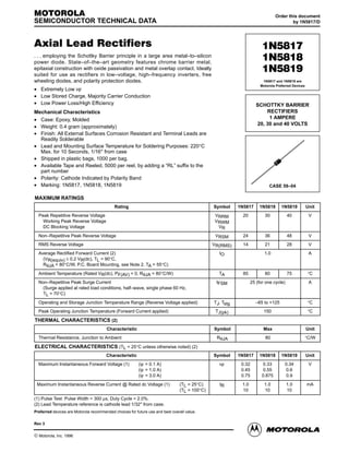
1N5817
40 30 23
60
80
RθJA (°C/W) = 110
125
115
105
95
85
75
2015107.05.0 304.03.0
40 30 23
RθJA (°C/W) = 110
80
60
Figure 2. Maximum Reference Temperature
1N5818
125
115
105
95
85
75
2015107.05.0 304.0 40
RθJA (°C/W) = 110
60
80
Figure 3. Maximum Reference Temperature
1N5819
Circuit
Load
Half Wave
Resistive Capacitive*
Full Wave, Bridge
Resistive Capacitive
Full Wave, Center Tapped*†
Resistive Capacitive
Sine Wave
Square Wave
0.5
0.75
1.3
1.5
0.5
0.75
0.65
0.75
1.0
1.5
1.3
1.5
40
30
23
TR,REFERENCETEMPERATURE(C)
°
VR, DC REVERSE VOLTAGE (VOLTS)
VR, DC REVERSE VOLTAGE (VOLTS)
*Note that VR(PK) ≈ 2.0 Vin(PK). †Use line to center tap voltage for Vin.
Table 1. Values for Factor F
TR,REFERENCETEMPERATURE(
°
C)
1N5817 1N5818 1N5819
2 Rectifier Device Data
NOTE 1 — DETERMINING MAXIMUM RATINGS
Reverse power dissipation and the possibility of thermal runaway
must be considered when operating this rectifier at reverse voltages
above 0.1 VRWM. Proper derating may be accomplished by use of
equation (1).
TA(max) =
where TA(max) =
TJ(max) =
PF(AV) =
PR(AV) =
RθJA =
TJ(max) – RθJAPF(AV) – RθJAPR(AV)
Maximum allowable ambient temperature
Maximum allowable junction temperature
(1)
Average forward power dissipation
(125°C or the temperature at which thermal
runaway occurs, whichever is lowest)
Average reverse power dissipation
Junction–to–ambient thermal resistance
Figures 1, 2, and 3 permit easier use of equation (1) by taking re-
verse power dissipation and thermal runaway into consideration. The
figures solve for a reference temperature as determined by equation
(2).
TR = TJ(max) – RθJAPR(AV) (2)
Substituting equation (2) into equation (1) yields:
TA(max) = TR – RθJAPF(AV) (3)
Inspection of equations (2) and (3) reveals that TR is the ambient
temperature at which thermal runaway occurs or where TJ = 125°C,
when forward power is zero. The transition from one boundary condi-
tion to the other is evident on the curves of Figures 1, 2, and 3 as a
differencein the rate of change of the slope in the vicinity of 115°C. The
dataof Figures 1, 2, and 3 is based upon dc conditions. For use in com-
mon rectifier circuits, Table 1 indicates suggested factors for an equiv-
alent dc voltage to use for conservative design, that is:
(4)VR(equiv) = Vin(PK) x F
The factor F is derived by considering the properties of the various rec-
tifier circuits and the reverse characteristics of Schottky diodes.
EXAMPLE:FindTA(max)for1N5818operatedina12–voltdcsupply
usingabridgecircuitwithcapacitivefiltersuchthatIDC=0.4A(IF(AV)=
0.5 A), I(FM)/I(AV) = 10, Input Voltage = 10 V(rms), RθJA = 80°C/W.
Step 1. Find VR(equiv). Read F = 0.65 from Table 1,
Step 1. Find ∴ VR(equiv) = (1.41)(10)(0.65) = 9.2 V.
Step 2. Find TR from Figure 2. Read TR = 109°C
Step 1. Find @ VR = 9.2 V and RθJA = 80°C/W.
Step 3. Find PF(AV) from Figure 4. **Read PF(AV) = 0.5 W
@
I(FM)
I(AV)
= 10 and IF(AV) = 0.5 A.
Step 4. Find TA(max) from equation (3).
Step 4. Find TA(max) = 109 – (80) (0.5) = 69°C.
**Values given are for the 1N5818. Power is slightly lower for the
1N5817 because of its lower forward voltage, and higher for the
1N5819.
3. 1N5817 1N5818 1N5819
3Rectifier Device Data
7/8
20
40
50
90
80
70
60
30
10
3/45/81/23/81/4 1.01/81
RθJL,THERMALRESISTANCE,JUNCTION–TO–LEAD(°C/W)
BOTH LEADS TO HEATSINK,
EQUAL LENGTH
MAXIMUM
TYPICAL
L, LEAD LENGTH (INCHES)
Figure 4. Steady–State Thermal Resistance
5.0
3.0
2.0
1.0
0.7
0.5
0.3
0.2
0.1
0.07
0.05
4.02.01.00.80.60.40.2
PF(AV),AVERAGEPOWERDISSIPATION(WATTS)
IF(AV), AVERAGE FORWARD CURRENT (AMP)
dc
SQUARE WAVE
TJ ≈ 125°C
1.0
0.7
0.5
0.3
0.2
0.1
0.07
0.05
0.03
0.02
0.01
10k2.0k1.0k5002001005020105.02.01.00.50.20.1 5.0k
r(t),TRANSIENTTHERMALRESISTANCE(NORMALIZED)
ZθJL(t) = ZθJL • r(t)
Ppk Ppk
tp
t1
TIME
DUTY CYCLE, D = tp/t1
PEAK POWER, Ppk, is peak of an
equivalent square power pulse.
∆TJL = Ppk • RθJL [D + (1 – D) • r(t1 + tp) + r(tp) – r(t1)]
where
∆TJL = the increase in junction temperature above the lead temperature
r(t) = normalized value of transient thermal resistance at time, t, from Figure 6, i.e.:
r(t) = r(t1 + tp) = normalized value of transient thermal resistance at time, t1 + tp.
t, TIME (ms)
NOTE 2 — MOUNTING DATA
Data shown for thermal resistance junction–to–ambient (RθJA) for
the mountings shown is to be used as typical guideline values for pre-
liminary engineering, or in case the tie point temperature cannot be
measured.
TYPICAL VALUES FOR RθJA IN STILL AIR
Mounting
Method 1/8 1/4 1/2 3/4
Lead Length, L (in)
RθJA
1
2
3
52
67
65
80
72
87
85
100
°C/W
°C/W
°C/W50
Mounting Method 1
P.C. Board with
1–1/2″ x 1–1/2″
copper surface.
Mounting Method 3
P.C. Board with
1–1/2″ x 1–1/2″
copper surface.
L L
L = 3/8″
BOARD GROUND
PLANE
VECTOR PIN MOUNTING
L L
Mounting Method 2
5
10
20
Sine Wave
I(FM)
I(AV)
= π (Resistive Load)
Capacitive
Loads {
Figure 5. Forward Power Dissipation
1N5817–19
Figure 6. Thermal Response
4. 1N5817 1N5818 1N5819
4 Rectifier Device Data
100705.0
125
115
105
95
85
75
207.0 103.02.0 301.0 40
15
5.0
3.0
2.0
0.3
0.2
0.1
403612
30
20
1.0
0.5
0.05
0.03
2416 208.04.0 280 32
10
20
7.0
5.0
2.0
0.2
0.3
0.5
0.7
1.0
3.0
0.9 1.0 1.1
0.1
0.07
0.05
0.03
0.02
0.60.50.40.30.2 0.70.1 0.8
NOTE 3 — THERMAL CIRCUIT MODEL
(For heat conduction through the leads)
TA(A) TA(K)
RθS(A) RθL(A) RθJ(A) RθJ(K) RθL(K) RθS(K)
PD
TL(A) TC(A) TJ TC(K) TL(K)
vF, INSTANTANEOUS FORWARD VOLTAGE (VOLTS)
iF,INSTANTANEOUSFORWARDCURRENT(AMP)
Figure 7. Typical Forward Voltage
IFSM,PEAKSURGECURRENT(AMP)
NUMBER OF CYCLES
Figure 8. Maximum Non–Repetitive Surge Current
IR,REVERSECURRENT(mA)
VR, REVERSE VOLTAGE (VOLTS)
Figure 9. Typical Reverse Current
TC = 100°C
25°C
1 Cycle
TL = 70°C
f = 60 Hz
Surge Applied at
Rated Load Conditions
1N5817
1N5818
1N5819
TJ = 125°C
100°C
25°C
Use of the above model permits junction to lead thermal resistance
for any mounting configuration to be found. For a given total lead
length, lowest values occur when one side of the rectifier is brought
as close as possible to the heatsink. Terms in the model signify:
TA = Ambient Temperature TC = Case Temperature
TL = Lead Temperature TJ = Junction Temperature
RθS = Thermal Resistance, Heatsink to Ambient
RθL = Thermal Resistance, Lead to Heatsink
RθJ = Thermal Resistance, Junction to Case
PD = Power Dissipation
(Subscripts A and K refer to anode and cathode sides, respectively.)
Values for thermal resistance components are:
RθL = 100°C/W/in typically and 120°C/W/in maximum
RθJ = 36°C/W typically and 46°C/W maximum.
75°C
5. 1N5817 1N5818 1N5819
5Rectifier Device Data
NOTE 4 — HIGH FREQUENCY OPERATION
Since current flow in a Schottky rectifier is the result of majority carri-
er conduction, it is not subject to junction diode forward and reverse re-
covery transients due to minority carrier injection and stored charge.
Satisfactory circuit analysis work may be performed by using a model
consistingof an ideal diode in parallel with a variable capacitance. (See
Figure 10.)
Rectification efficiency measurements show that operation will be
satisfactory up to several megahertz. For example, relative waveform
rectification efficiency is approximately 70 percent at 2.0 MHz, e.g., the
ratio of dc power to RMS power in the load is 0.28 at this frequency,
whereas perfect rectification would yield 0.406 for sine wave inputs.
However, in contrast to ordinary junction diodes, the loss in waveform
efficiency is not indicative of power loss: it is simply a result of reverse
current flow through the diode capacitance, which lowers the dc output
voltage.
10 200.8
70
200
100
50
30
20
10
6.04.02.01.00.6 8.00.4 40
C,CAPACITANCE(pF)
VR, REVERSE VOLTAGE (VOLTS)
Figure 10. Typical Capacitance
TJ = 25°C
f = 1.0 MHz
1N5819
1N5818
1N5817
6. 1N5817 1N5818 1N5819
6 Rectifier Device Data
PACKAGE DIMENSIONS
ISSUE M
CASE 59–04
K
A
D
K
B
DIM MIN MAX MIN MAX
INCHESMILLIMETERS
A 5.97 6.60 0.235 0.260
B 2.79 3.05 0.110 0.120
D 0.76 0.86 0.030 0.034
K 27.94 ––– 1.100 –––
NOTES:
1. ALL RULES AND NOTES ASSOCIATED WITH
JEDEC DO–41 OUTLINE SHALL APPLY.
2. POLARITY DENOTED BY CATHODE BAND.
3. LEAD DIAMETER NOT CONTROLLED WITHIN F
DIMENSION.
Motorola reserves the right to make changes without further notice to any products herein. Motorola makes no warranty, representation or guarantee regarding
the suitability of its products for any particular purpose, nor does Motorola assume any liability arising out of the application or use of any product or circuit, and
specifically disclaims any and all liability, including without limitation consequential or incidental damages. “Typical” parameters which may be provided in Motorola
datasheetsand/orspecificationscananddovaryindifferentapplicationsandactualperformancemayvaryovertime. Alloperatingparameters,including“Typicals”
must be validated for each customer application by customer’s technical experts. Motorola does not convey any license under its patent rights nor the rights of
others. Motorola products are not designed, intended, or authorized for use as components in systems intended for surgical implant into the body, or other
applicationsintended to support or sustain life, or for any other application in which the failure of the Motorola product could create a situation where personal injury
ordeath may occur. ShouldBuyerpurchaseoruseMotorolaproductsforanysuchunintendedorunauthorizedapplication,BuyershallindemnifyandholdMotorola
and its officers, employees, subsidiaries, affiliates, and distributors harmless against all claims, costs, damages, and expenses, and reasonable attorney fees
arising out of, directly or indirectly, any claim of personal injury or death associated with such unintended or unauthorized use, even if such claim alleges that
Motorola was negligent regarding the design or manufacture of the part. Motorola and are registered trademarks of Motorola, Inc. Motorola, Inc. is an Equal
Opportunity/Affirmative Action Employer.
Mfax is a trademark of Motorola, Inc.
How to reach us:
USA/EUROPE/Locations Not Listed: Motorola Literature Distribution; JAPAN: Nippon Motorola Ltd.; Tatsumi–SPD–JLDC, 6F Seibu–Butsuryu–Center,
P.O. Box 5405, Denver, Colorado 80217. 303–675–2140 or 1–800–441–2447 3–14–2 Tatsumi Koto–Ku, Tokyo 135, Japan. 81–3–3521–8315
Mfax™: RMFAX0@email.sps.mot.com – TOUCHTONE 602–244–6609 ASIA/PACIFIC: Motorola Semiconductors H.K. Ltd.; 8B Tai Ping Industrial Park,
INTERNET: http://Design–NET.com 51 Ting Kok Road, Tai Po, N.T., Hong Kong. 852–26629298
1N5817/D◊