Download as PDF, PPTX

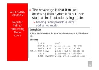
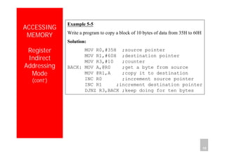
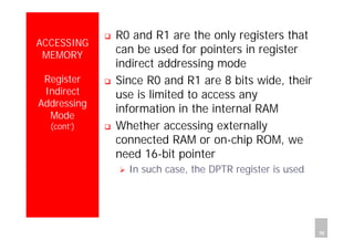

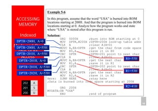
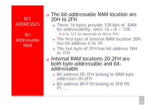
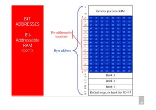
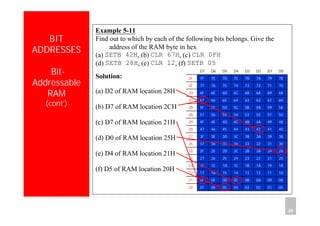

This document discusses various addressing modes of the 8051 microcontroller including immediate, register, direct, register indirect, indexed, and their applications. It provides examples of using different addressing modes to access memory locations and special function registers. Register indirect addressing mode allows dynamic access of memory using pointer registers R0 and R1 while indexed addressing is used to access on-chip ROM by combining the contents of register A with the 16-bit data pointer register DPTR.