Download to read offline

![ISSN: 2277 – 9043
International Journal of Advanced Research in Computer Science and Electronics Engineering (IJARCSEE)
Volume 1, Issue 6, August 2012
Form the above mention formula, the condition arises [11] M. E. Goldforb and R. A. Pucel, “Modding Via Hole Grounds
in Microstrip,” IEEE Microwave and Guided Ware Letters,
R C L G for distortion less transmission line. Since Vol.1, No. 6, PP. 135-137, June 1991.
there is no wires or long conducting element L and G [12] M. Kahrizi, K. Sarkar and Zoran A. Maricevic, “Dynamic
Analysis of a Microstrip Line Over a Perforated Ground Plane”,
cannot be changed so it is very evident from the above IEEE Transaction on Microwave Theory and Techniques, Vol.
condition that only R and C can be inversely proportional 42, No. 5, May 1994.
[13] N. Jain and B. Brown, “Dispersion Characteristics of
to each other as C is dependent on relative permittivity and Microstrip Transmission line on Glass Microwave IC’S”, IEEE
R can be treated as characteristic impedance it can be Microwave and Guided Wave Letter, Vol. 7, No. 10, Oct. 1997.
[14] R.J. Akello, B. Easter, and I.M. Stephenson, “Equivalent
knuckled with the fact that whenever C Increases R circuit of the symmetric crossover junction,
decreases. “Electronics Letters, vol.13,no.4,PP.117-118, Feb 1977.
V. CONCLUSION
Work has been done to demonstrate the utility of microstrip
line and its advantages especially energy is to be transferred
from one point to another, in a very compact and efficient AUTHOR’S PROFILE
form. A simple and inexpensive method also known as
quasi-static has been applied for calculating the Akanksha lal is working as a Asst. Prof. in the Department of
Electronics & Communication Engineering in SHIATS, Allahabad. She
characteristic impedance as well as effective permittivity. received her M.Tech. Degree in Advanced Communication Systems
Variation of characteristic impedance for different value of Engineering from SHIATS, Allahabad in 2010. His research is focused on
normalized strip width as well as different value of effective Microwave Engineering,Wireless communication.
Mukesh Kumar is working as a Asst. Prof. in the Department of
permittivity is represented. It has been observed that Electronics & Communication Engineering in SHIATS, Allahabad. He
characteristic impedance decreases with advancement of received his M.Tech. Degree in Advanced Communication Systems
normalized strip width and also decreases for increasing Engineering from SHIATS, Allahabad in 2010. His research is focused on
Microwave Engineering, Wireless Sensors Networks and Computer
effective permittivity. This property can be applied in Networks as well as Optical fiber communication.
microwave transmission theory to design different antenna Rohini Saxena is working as a Asst. Prof. in the Department of
models for different purposes along with the advantage of Electronics & Communication Engineering in SHIATS, Allahabad. She
received her M.Tech. Degree in Advanced Communication Systems
minimal distortion, and avoiding high cross-talk and Engineering from SHIATS, Allahabad in 2009. His research is focused on
radiation. Microwave Engineering, Wireless Sensors Networks and Computer
Networks and Mobile communication.
VI. REFRENCES
.
[1] Baklem and A. Dmar, “Invarted Defected Ground Structure for
Microstrip line filter reducing Packaging Complicity,
Department of Electrical, Czech Technical University, 2008.
[2] A. Z. Elsherbeni, C. E. Smith and B. Moumnch, “Minimization
of the Coupling between a two Conductor Mirostrip
Transmission Line using Finite difference Method”, Journal of
Electromagnetic Waves and Application, Vol. 10, No. 4, 509-
513, 1006.
[3] B. Easter, “The Equivalent Circuit of some Microstrip
Discontinuities”, IEEE Transaction on Microwave Theory and
Techniques, Vol. 23, No. 8, PP.655-660 Aug. 1975.
[4] C. K. Wu and H. S. Wu, “Electric- Magnetic- Electric Slow-
Wave Microstrip Line and Bond pass Filter of Compressed
Size”, IEEE Transaction on Microwave Theory and Techniques,
Vol. 50, No. 8, Aug, 2002.
[5] E. Tunier. Lee B. T., M. Islam and D. P. Nickirk, “Quasi-Static
Conductor Loss Calculations in Transmission Theory and
Techniques, Vol. 42, PP. 1807-1815, 1994.
[6] E. Tunnier, and P. Nickirk, “Highly Accurate Quasi-Static
Modding of Microstrip Lines over Lossy Subptrates”, IEEE
Microwave and Guided Wave Letter, Vol. 2, No. 10, October
1992.
[7] E. Yamshita, “Variational Method for the Analysis of
Microstrip Like Transmission Lines”, IEEE Transaction on
Microwave Theory and Techniques, Vol. 16 No. 8, Aug, 1968.
[8] H. Wang, Y. Ji, and T. H. Hubiay, “Experimental and
Numerical study of the Radiation from Microstrip Bends”,
University of Missouri-Rolla, 2000.
[9] J. C. Rautis, and V. Demir, “Microstrip Conductor loss Models
for Electro-Magnetic Analysis”, IEEE Transaction on
Microwave Theory and Techniques, Vol. 51, No. 3, March.
2003.
[10] J. S. Lim, C.S. Kim and J. S. Park, “Design of 10.1B 900
Branch Line Coupler using Microstrip Line with defected
ground Structure”, Electronics Letters, Vol. 56, No. 21, Oct.
2000.
133](https://image.slidesharecdn.com/130-133-120825221757-phpapp01/85/130-133-4-320.jpg)

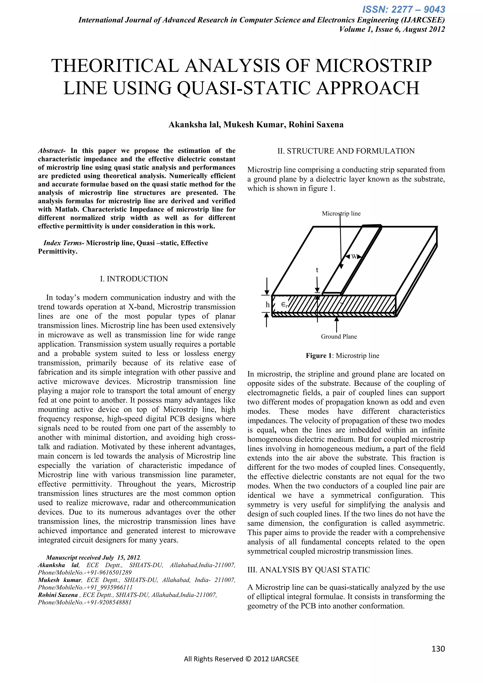
The document analyzes microstrip transmission lines using a quasi-static approach. It presents numerically efficient and accurate formulas to analyze microstrip line structures. The analysis derives formulas for characteristic impedance of microstrip lines based on variables like the normalized strip width, effective permittivity, height of the substrate, and thickness of the microstrip line. It also defines the structure of a microstrip line and formulates the quasi-static analysis by introducing the concept of an effective relative dielectric constant to account for the microstrip being surrounded by different dielectrics like air and the substrate material.