Download to read offline


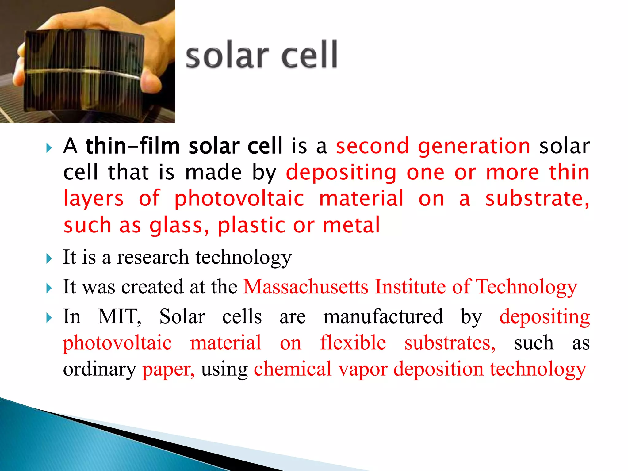


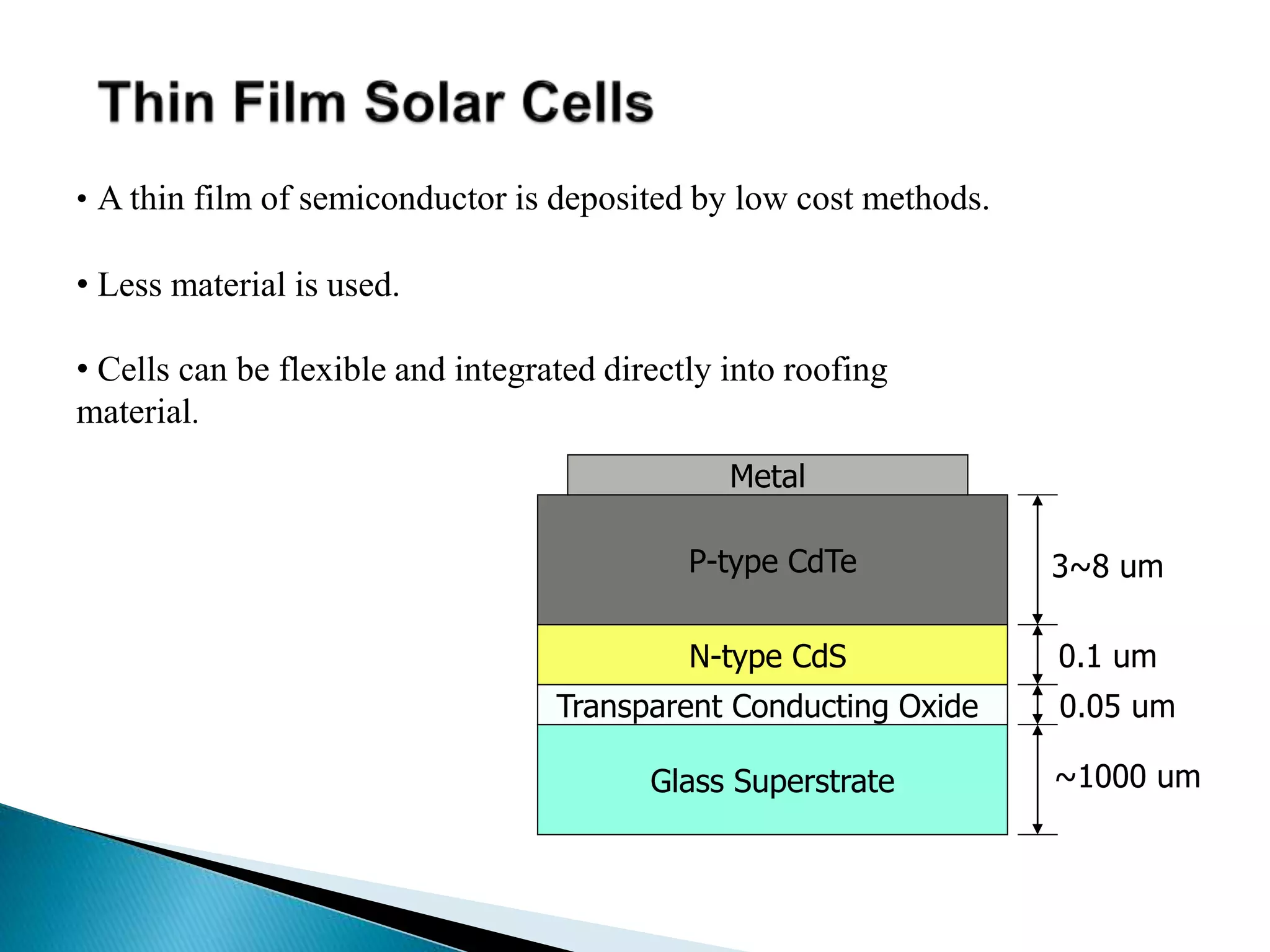

This document discusses thin-film solar cells, which are made by depositing one or more thin layers of photovoltaic material onto a substrate using techniques like chemical vapor deposition. It was developed at MIT using this process to deposit materials onto flexible substrates like paper. Chemical vapor deposition is used to produce high-quality solid thin films and is commonly used in the semiconductor industry. Thin-film solar cells aim to reduce costs compared to conventional solar panels by using less material and creating lightweight, flexible designs.


