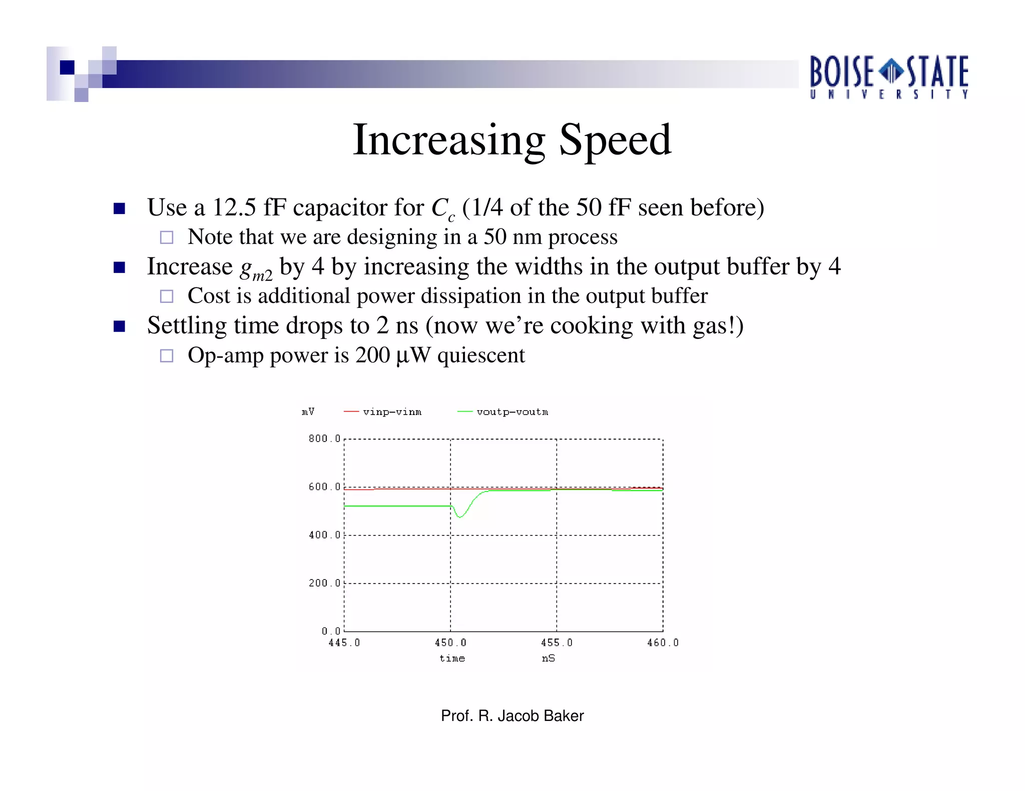
Prof. R. Jacob Baker
Design of High-Speed Op-Amps for Signal Processing
R. Jacob (Jake) Baker, PhD, PE
Professor and Chair
Boise State University
1910 University Dr.
Boise, ID 83725-2075
jbaker@ieee.org
Abstract - As CMOS gate lengths scale to tens of nanometers open circuit gains drop
and analog circuit design techniques that minimize the need for good matching
become critical. This talk presents techniques useful for implementing high-speed
CMOS op-amps for signal processing (e.g. analog-to-digital converters, filters,
input receivers, etc.) in nanometer size CMOS. Techniques for biasing, device size
selection, topologies, and compensation are discussed. Design examples are
presented and used in system level building blocks. The emphasis is on practical
design where power, speed, and manufacturability are critical.
Prof. R. Jacob Baker
Background and Content
This talk assumes a background in CMOS op-amp design
Biasing using current mirrors
Know basics of op-amp design, e.g., compensating two-stage op-amps
Calculation of small-signal gains
The content of this talk is from: CMOS Circuit Design,
Layout, and Simulation, Second Edition, Wiley-IEEE, 2005.
http://cmosedu.com (for the book’s figures and simulation netlists)
Prof. R. Jacob Baker
Design with nm devices (here we use a 50 nm process)
Key points
Devices do not follow the square-law equations (so don’t use them)!
Nanometer CMOS is characterized using:
On current
Off current
VDD
Gate oxide capacitance
Plots of measured data (note equations can’t be used; too complicated for
hand calculations).
Prof. R. Jacob Baker
Long Channel IV curves
Prof. R. Jacob Baker
Transition frequency
FOM (figure of merit) for CMOS amplifier design
Important!!!
Prof. R. Jacob Baker
Biasing for high speed
Must use minimum length devices
Matching becomes even more important
Larger overdrive results in faster circuits
Drawback is that the devices enter the triode region earlier
For minimum power use mimimum size devices
For nm CMOS minimum (drawn) W is, generally, 10 times minimum L
Use for NMOS 10/1 and for PMOS, to match drive, 20/1
Concerns
Is there enough drive using minimum-size devices?
Matching!!!
Prof. R. Jacob Baker
Examples for general design
Use 2 to 5 times minimum L (use minimum L for high-speed)
Increases open circuit gain (output resistance)
Using longer L improves matching
Use overdrive voltage that is 5% of VDD
Increase for high-speed design (say 10% of VDD)
Table on the next page shows typical parameters for general
design
Prof. R. Jacob Baker
Bias current (overdrive) and gain
Prof. R. Jacob Baker
Biasing
Temperature stability
Power supply insensitive
Good variations with process
Sets the overdrive voltages in the design
Need a self-biased reference; a beta multiplier reference
(BMR)
Prof. R. Jacob Baker
Problems with BMRs in nm CMOS
Prof. R. Jacob Baker
BMR for nm CMOS
Prof. R. Jacob Baker
Circuit implementation of a BMR in nm CMOS
Prof. R. Jacob Baker
Stability is Critical for this design
Removing the capacitors causes the reference to oscillate.
Prof. R. Jacob Baker
Generating Bias Voltages for nm Design
Prof. R. Jacob Baker
Performance of Cascode Current Mirrors
Prof. R. Jacob Baker
Output Buffer with Bias Voltages
Prof. R. Jacob Baker
Two-Stage Op-Amp with Miller Compensation
Simple topology using diff-amp and common-source amplifier
Can’t drive resistive loads
Poor PSRR
Using Miller compensation
Poor PSRR
Have that pesky right-half plane zero
Slow-speed (unless you use bias with large devices and currents) for a
given load C
Poor slewing
Prof. R. Jacob Baker
Example of a bad (academic) op-amp design
Prof. R. Jacob Baker
AC Response of this bad design with Rz = 0 and Cc = 2.4 pF
Prof. R. Jacob Baker
Step response of the bad design
Prof. R. Jacob Baker
Making the Op-Amp more Stable
Obviously we can increase Rz to move the zero into the LHP
Controlling the value of Rz becomes challenging over temperature and
process
The stability is becoming a problem because the pole
associated with the op-amp’s output, f2 , is too low.
Increase f2 by increasing the gm of the output stage (gm2).
Increase widths of the devices so overdrive stays constant (ID goes up)!
In general, make sure overdrive voltages are the same in all MOSFETs!
Prof. R. Jacob Baker
Practical Way to Compensate an Op-Amp
Never use Miller Compensation
Never, ever, connect a compensation capacitor between two high-
impedance nodes!!! (unless you want slow speed)
The literature is filled with examples of how not to compensate op-amps
for high speed operation
We’ll develop Indirect Feedback Compensation in the next
few pages
Practical way to compensate an op-amp
Feedback a current indirectly to the output of the diff-amp via:
MOSFETs laid out in series (one operating in the triode region)
A common-gate amplifier
A cascode structure
Better PSRR
Smaller layout area (compensation capacitor reduced 4 to 10 times)
Much faster!!!
Prof. R. Jacob Baker
Indirect Feedback Compensation
Current through Cc
We’ll use this. How?
Prof. R. Jacob Baker
Using Triode Operating MOSFETs
Triode-operating MOSFETs.
100/2 laid out as two 100/1
High-impedance node
Prof. R. Jacob Baker
Other examples of Indirect Feedback Compensation
Using a common-gate amplifier Using a cascode structure
Prof. R. Jacob Baker
Other examples of Indirect Feedback Compensation, cont’d
Using NMOS triode-operating diff-pair for good PSRR
Triode-operating MOSFETs.
50/2 laid out as two 50/1
in series.
Prof. R. Jacob Baker
Equations
RHP zero eliminated. A LHP zero is introduced.The
LHP zero increases the phase-margin and speed.
Equation for the unity gain frequency remains the same.
However, the value goes up because Cc can drop by 4 to 10
Cc drops because load C has less effect on f2
Prof. R. Jacob Baker
Example (next page) Two-Stage Op-Amp
Cascode input stage (sometimes called a telescopic input
stage)
Use a push-pull output stage for rail-to-rail output swing
Indirect feedback compensation
> 100 MHz gain-bandwidth product while using 250 µA and a
VDD of 1 V (excluding the bias circuit power is 250 µW)
Excellent PSRR
Compact layout area
Prof. R. Jacob Baker
A Practical General Purpose Op-Amp
Prof. R. Jacob Baker
Step Response
Previous page
Prof. R. Jacob Baker
Comments
We were careful to select overdrive voltages for a specific
speed (transition frequency)
Important to avoid adding a low-frequency pole in the transfer function
and thus having a non-optimized design
Fiddling with widths while not keeping the overdrive voltages constant
is a path to low-quality designs
In general, only vary lengths of MOSFETs in DC circuits
To push f2 to a higher frequency we increase the widths of the
output stage (gm2 and current in output stage are increased)
Reducing Cc causes the gain-bandwidth product, fun, to
increase (and move towards f2).
Prof. R. Jacob Baker
Bad Output Stage Design
Not controlling current in the output stage leads to:
Bad input-referred offset
Potential for large power dissipation
Not controlling output stages gm (and thus stability)
Don’t let SPICE fool you into thinking you can actually set the
current in an output buffer without using current mirrors (you
can’t!)
Prof. R. Jacob Baker
Example (bad) Output Stages
If M7 mirrors current in M4 then M8 triodes and the gain drops.
The gate of M7 will have to drop, with the negative feedback
around the op-amp (so M8 operates in saturation). The result is a
huge current flowing in the inverter output stage.
Prof. R. Jacob Baker
Bad Output Stage Design Cont’d
Source follower is used to allow the gate of M8 to drop to a lower voltage
so that, hopefully, it can remain in saturation during normal operation.
Again, however, we are not controlling the current in the output stage. It
may be small, big, or exactly what we want (again, don’t let SPICE fool you
into thinking this type of design is okay (it’s not!)
Prof. R. Jacob Baker
Bad Diff-Amp Biasing
Never design a diff-amp where the PMOS current sources fight against
NMOS current sources. The outputs will float up or down causing some
MOSFETs to triode.
Prof. R. Jacob Baker
Add Control to a Diff-Amp to Set Currents
The added control ensures the current sourced by the PMOS equals the
current sunk by the NMOS. Controls common-mode output voltage via
common-mode feedback (CMFB).
Prof. R. Jacob Baker
Op-Amps in Signal Processing
Use fully-differential inputs and outputs
Reduces the common-mode noise
Need to employ common-mode feedback (CMFB)
Our examples here will use switched capacitor CMFB and two
stage op-amps (for the lowest power and highest speed)
Fully-differential topologies offer the benefit that class AB
output buffers can be implemented without floating current
sources
Don’t need the additional bias circuits
Prof. R. Jacob Baker
Basic Fully-Differential Op-amp
Prof. R. Jacob Baker
Need to set output common-mode level
Prof. R. Jacob Baker
Switched-Capacitor CMFB
Prof. R. Jacob Baker
Use of SC-CMFB
For the most robust design used SC-CMFB around each stage
The outputs of the diff-amp are set to bias the output buffer
The outputs of the buffer (the op-amp outputs) are balanced around the
common-mode voltage, VCM
SC-CMFB provides wide operating range
Low power consumption
Small loading
Robust operation
Prof. R. Jacob Baker
Example: a S/H amplifier
Prof. R. Jacob Baker
Input Diff-Amp
Prof. R. Jacob Baker
Setting the Output CM Level – method to get
proper biasing with horrible offsets
Prof. R. Jacob Baker
Output Stage
Prof. R. Jacob Baker
Simulating the Op-Amp’s Operation
No compensation capacitance (unstable in some cases), settling approx. 6 ns
Note that these simulation results are directly from Fig. 26.60 in my CMOS book, see
http://cmosedu.com
Prof. R. Jacob Baker
Increasing Compensation Cap to 50 fF
The settling time is approximately 5 ns. Note the stability is, of course, better.
Direct sim of Fig. 26.60 except the rise/fall times of the clock signals was reduced from 2
ns to 200 ps (this slows the simulation time)
Prof. R. Jacob Baker
Increasing Compensation Cap to 150 fF
Better stability but longer settling time. What do we do?
Prof. R. Jacob Baker
Increasing speed (decreasing settling time)
We need to increase the gain bandwidth product of the op-amp
The only ways to do this are to decrease the compensation capacitor
and/or increase the diff-amp’s transconductance, fun = gm/2πCc
The problem with this, as just shown, is stability (the pole, f2
associated with the output of the op-amp is comparable to fun)
Need to push f2 to a higher frequency by increasing the output buffers
gm
We do this by increasing the widths of the devices in the output buffer
Note this results in larger current flowing in the output buffers keeping
overdrive voltages constant (important)
To increase the gm of the diff-pair we increase their widths
Prof. R. Jacob Baker
Increasing Speed
Use a 12.5 fF capacitor for Cc (1/4 of the 50 fF seen before)
Note that we are designing in a 50 nm process
Increase gm2 by 4 by increasing the widths in the output buffer by 4
Cost is additional power dissipation in the output buffer
Settling time drops to 2 ns (now we’re cooking with gas!)
Op-amp power is 200 µW quiescent
Prof. R. Jacob Baker
Conclusions: Further Increases in Speed
(comments)
Why didn’t we try to increase speed by increasing the diff-
pair’s gm (by increasing the pair’s widths)?
This causes the overdrive voltages of the diff-pair to decrease unless we
increase the diff-pair bias current (which would require increasing the
widths of other devices in order to maintain the overdrive voltages). The
drop in the widths of the diff-pair cause (low) parasitic poles in op-
amp’s frequency response.
Small increases in diff-pair width are okay. We used a factor of 3 in the
sims here, that is, the diff-pair were 30/1 while other NMOS were 10/1.
Note, again, that we attempt to design with fixed overdrive
voltages to keep the design optimized for speed
Prof. R. Jacob Baker
Conclusions: Further Increases in Speed
(comments continued)
Looking at these results we might ask, “Why not multiple the
sizes in the output buffer by 8 and divide the compensation
capacitor by 8?”
We run into a brick wall. The parasitic poles of the devices
limit further increases in speed.
To obviate this limitation we must increase the device’s transition
frequency (by increasing the overdrive voltages…change the bias
circuit)
Note we are assuming minimum L devices (absolutely necessary for
high-speed design)

Ieee eds wmed_2005

  • 1.
    Prof. R. JacobBaker Design of High-Speed Op-Amps for Signal Processing R. Jacob (Jake) Baker, PhD, PE Professor and Chair Boise State University 1910 University Dr. Boise, ID 83725-2075 jbaker@ieee.org Abstract - As CMOS gate lengths scale to tens of nanometers open circuit gains drop and analog circuit design techniques that minimize the need for good matching become critical. This talk presents techniques useful for implementing high-speed CMOS op-amps for signal processing (e.g. analog-to-digital converters, filters, input receivers, etc.) in nanometer size CMOS. Techniques for biasing, device size selection, topologies, and compensation are discussed. Design examples are presented and used in system level building blocks. The emphasis is on practical design where power, speed, and manufacturability are critical.
  • 2.
    Prof. R. JacobBaker Background and Content This talk assumes a background in CMOS op-amp design Biasing using current mirrors Know basics of op-amp design, e.g., compensating two-stage op-amps Calculation of small-signal gains The content of this talk is from: CMOS Circuit Design, Layout, and Simulation, Second Edition, Wiley-IEEE, 2005. http://cmosedu.com (for the book’s figures and simulation netlists)
  • 3.
    Prof. R. JacobBaker Design with nm devices (here we use a 50 nm process) Key points Devices do not follow the square-law equations (so don’t use them)! Nanometer CMOS is characterized using: On current Off current VDD Gate oxide capacitance Plots of measured data (note equations can’t be used; too complicated for hand calculations).
  • 4.
    Prof. R. JacobBaker Long Channel IV curves
  • 5.
    Prof. R. JacobBaker Transition frequency FOM (figure of merit) for CMOS amplifier design Important!!!
  • 6.
    Prof. R. JacobBaker Biasing for high speed Must use minimum length devices Matching becomes even more important Larger overdrive results in faster circuits Drawback is that the devices enter the triode region earlier For minimum power use mimimum size devices For nm CMOS minimum (drawn) W is, generally, 10 times minimum L Use for NMOS 10/1 and for PMOS, to match drive, 20/1 Concerns Is there enough drive using minimum-size devices? Matching!!!
  • 7.
    Prof. R. JacobBaker Examples for general design Use 2 to 5 times minimum L (use minimum L for high-speed) Increases open circuit gain (output resistance) Using longer L improves matching Use overdrive voltage that is 5% of VDD Increase for high-speed design (say 10% of VDD) Table on the next page shows typical parameters for general design
  • 8.
  • 9.
    Prof. R. JacobBaker Bias current (overdrive) and gain
  • 10.
    Prof. R. JacobBaker Biasing Temperature stability Power supply insensitive Good variations with process Sets the overdrive voltages in the design Need a self-biased reference; a beta multiplier reference (BMR)
  • 11.
    Prof. R. JacobBaker Problems with BMRs in nm CMOS
  • 12.
    Prof. R. JacobBaker BMR for nm CMOS
  • 13.
    Prof. R. JacobBaker Circuit implementation of a BMR in nm CMOS
  • 14.
    Prof. R. JacobBaker Stability is Critical for this design Removing the capacitors causes the reference to oscillate.
  • 15.
    Prof. R. JacobBaker Generating Bias Voltages for nm Design
  • 16.
    Prof. R. JacobBaker Performance of Cascode Current Mirrors
  • 17.
    Prof. R. JacobBaker Output Buffer with Bias Voltages
  • 18.
    Prof. R. JacobBaker Two-Stage Op-Amp with Miller Compensation Simple topology using diff-amp and common-source amplifier Can’t drive resistive loads Poor PSRR Using Miller compensation Poor PSRR Have that pesky right-half plane zero Slow-speed (unless you use bias with large devices and currents) for a given load C Poor slewing
  • 19.
    Prof. R. JacobBaker Example of a bad (academic) op-amp design
  • 20.
    Prof. R. JacobBaker AC Response of this bad design with Rz = 0 and Cc = 2.4 pF
  • 21.
    Prof. R. JacobBaker Step response of the bad design
  • 22.
    Prof. R. JacobBaker Making the Op-Amp more Stable Obviously we can increase Rz to move the zero into the LHP Controlling the value of Rz becomes challenging over temperature and process The stability is becoming a problem because the pole associated with the op-amp’s output, f2 , is too low. Increase f2 by increasing the gm of the output stage (gm2). Increase widths of the devices so overdrive stays constant (ID goes up)! In general, make sure overdrive voltages are the same in all MOSFETs!
  • 23.
    Prof. R. JacobBaker Practical Way to Compensate an Op-Amp Never use Miller Compensation Never, ever, connect a compensation capacitor between two high- impedance nodes!!! (unless you want slow speed) The literature is filled with examples of how not to compensate op-amps for high speed operation We’ll develop Indirect Feedback Compensation in the next few pages Practical way to compensate an op-amp Feedback a current indirectly to the output of the diff-amp via: MOSFETs laid out in series (one operating in the triode region) A common-gate amplifier A cascode structure Better PSRR Smaller layout area (compensation capacitor reduced 4 to 10 times) Much faster!!!
  • 24.
    Prof. R. JacobBaker Indirect Feedback Compensation Current through Cc We’ll use this. How?
  • 25.
    Prof. R. JacobBaker Using Triode Operating MOSFETs Triode-operating MOSFETs. 100/2 laid out as two 100/1 High-impedance node
  • 26.
    Prof. R. JacobBaker Other examples of Indirect Feedback Compensation Using a common-gate amplifier Using a cascode structure
  • 27.
    Prof. R. JacobBaker Other examples of Indirect Feedback Compensation, cont’d Using NMOS triode-operating diff-pair for good PSRR Triode-operating MOSFETs. 50/2 laid out as two 50/1 in series.
  • 28.
    Prof. R. JacobBaker Equations RHP zero eliminated. A LHP zero is introduced.The LHP zero increases the phase-margin and speed. Equation for the unity gain frequency remains the same. However, the value goes up because Cc can drop by 4 to 10 Cc drops because load C has less effect on f2
  • 29.
    Prof. R. JacobBaker Example (next page) Two-Stage Op-Amp Cascode input stage (sometimes called a telescopic input stage) Use a push-pull output stage for rail-to-rail output swing Indirect feedback compensation > 100 MHz gain-bandwidth product while using 250 µA and a VDD of 1 V (excluding the bias circuit power is 250 µW) Excellent PSRR Compact layout area
  • 30.
    Prof. R. JacobBaker A Practical General Purpose Op-Amp
  • 31.
    Prof. R. JacobBaker Step Response Previous page
  • 32.
    Prof. R. JacobBaker Comments We were careful to select overdrive voltages for a specific speed (transition frequency) Important to avoid adding a low-frequency pole in the transfer function and thus having a non-optimized design Fiddling with widths while not keeping the overdrive voltages constant is a path to low-quality designs In general, only vary lengths of MOSFETs in DC circuits To push f2 to a higher frequency we increase the widths of the output stage (gm2 and current in output stage are increased) Reducing Cc causes the gain-bandwidth product, fun, to increase (and move towards f2).
  • 33.
    Prof. R. JacobBaker Bad Output Stage Design Not controlling current in the output stage leads to: Bad input-referred offset Potential for large power dissipation Not controlling output stages gm (and thus stability) Don’t let SPICE fool you into thinking you can actually set the current in an output buffer without using current mirrors (you can’t!)
  • 34.
    Prof. R. JacobBaker Example (bad) Output Stages If M7 mirrors current in M4 then M8 triodes and the gain drops. The gate of M7 will have to drop, with the negative feedback around the op-amp (so M8 operates in saturation). The result is a huge current flowing in the inverter output stage.
  • 35.
    Prof. R. JacobBaker Bad Output Stage Design Cont’d Source follower is used to allow the gate of M8 to drop to a lower voltage so that, hopefully, it can remain in saturation during normal operation. Again, however, we are not controlling the current in the output stage. It may be small, big, or exactly what we want (again, don’t let SPICE fool you into thinking this type of design is okay (it’s not!)
  • 36.
    Prof. R. JacobBaker Bad Diff-Amp Biasing Never design a diff-amp where the PMOS current sources fight against NMOS current sources. The outputs will float up or down causing some MOSFETs to triode.
  • 37.
    Prof. R. JacobBaker Add Control to a Diff-Amp to Set Currents The added control ensures the current sourced by the PMOS equals the current sunk by the NMOS. Controls common-mode output voltage via common-mode feedback (CMFB).
  • 38.
    Prof. R. JacobBaker Op-Amps in Signal Processing Use fully-differential inputs and outputs Reduces the common-mode noise Need to employ common-mode feedback (CMFB) Our examples here will use switched capacitor CMFB and two stage op-amps (for the lowest power and highest speed) Fully-differential topologies offer the benefit that class AB output buffers can be implemented without floating current sources Don’t need the additional bias circuits
  • 39.
    Prof. R. JacobBaker Basic Fully-Differential Op-amp
  • 40.
    Prof. R. JacobBaker Need to set output common-mode level
  • 41.
    Prof. R. JacobBaker Switched-Capacitor CMFB
  • 42.
    Prof. R. JacobBaker Use of SC-CMFB For the most robust design used SC-CMFB around each stage The outputs of the diff-amp are set to bias the output buffer The outputs of the buffer (the op-amp outputs) are balanced around the common-mode voltage, VCM SC-CMFB provides wide operating range Low power consumption Small loading Robust operation
  • 43.
    Prof. R. JacobBaker Example: a S/H amplifier
  • 44.
    Prof. R. JacobBaker Input Diff-Amp
  • 45.
    Prof. R. JacobBaker Setting the Output CM Level – method to get proper biasing with horrible offsets
  • 46.
    Prof. R. JacobBaker Output Stage
  • 47.
    Prof. R. JacobBaker Simulating the Op-Amp’s Operation No compensation capacitance (unstable in some cases), settling approx. 6 ns Note that these simulation results are directly from Fig. 26.60 in my CMOS book, see http://cmosedu.com
  • 48.
    Prof. R. JacobBaker Increasing Compensation Cap to 50 fF The settling time is approximately 5 ns. Note the stability is, of course, better. Direct sim of Fig. 26.60 except the rise/fall times of the clock signals was reduced from 2 ns to 200 ps (this slows the simulation time)
  • 49.
    Prof. R. JacobBaker Increasing Compensation Cap to 150 fF Better stability but longer settling time. What do we do?
  • 50.
    Prof. R. JacobBaker Increasing speed (decreasing settling time) We need to increase the gain bandwidth product of the op-amp The only ways to do this are to decrease the compensation capacitor and/or increase the diff-amp’s transconductance, fun = gm/2πCc The problem with this, as just shown, is stability (the pole, f2 associated with the output of the op-amp is comparable to fun) Need to push f2 to a higher frequency by increasing the output buffers gm We do this by increasing the widths of the devices in the output buffer Note this results in larger current flowing in the output buffers keeping overdrive voltages constant (important) To increase the gm of the diff-pair we increase their widths
  • 51.
    Prof. R. JacobBaker Increasing Speed Use a 12.5 fF capacitor for Cc (1/4 of the 50 fF seen before) Note that we are designing in a 50 nm process Increase gm2 by 4 by increasing the widths in the output buffer by 4 Cost is additional power dissipation in the output buffer Settling time drops to 2 ns (now we’re cooking with gas!) Op-amp power is 200 µW quiescent
  • 52.
    Prof. R. JacobBaker Conclusions: Further Increases in Speed (comments) Why didn’t we try to increase speed by increasing the diff- pair’s gm (by increasing the pair’s widths)? This causes the overdrive voltages of the diff-pair to decrease unless we increase the diff-pair bias current (which would require increasing the widths of other devices in order to maintain the overdrive voltages). The drop in the widths of the diff-pair cause (low) parasitic poles in op- amp’s frequency response. Small increases in diff-pair width are okay. We used a factor of 3 in the sims here, that is, the diff-pair were 30/1 while other NMOS were 10/1. Note, again, that we attempt to design with fixed overdrive voltages to keep the design optimized for speed
  • 53.
    Prof. R. JacobBaker Conclusions: Further Increases in Speed (comments continued) Looking at these results we might ask, “Why not multiple the sizes in the output buffer by 8 and divide the compensation capacitor by 8?” We run into a brick wall. The parasitic poles of the devices limit further increases in speed. To obviate this limitation we must increase the device’s transition frequency (by increasing the overdrive voltages…change the bias circuit) Note we are assuming minimum L devices (absolutely necessary for high-speed design)