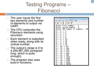
The document describes a project to design a microcontroller that supports the instruction set of the Motorola 68HC12 microcontroller using VHDL. Key aspects of the project include:
- Implementing the 68HC12 instruction set and addressing modes on an FPGA.
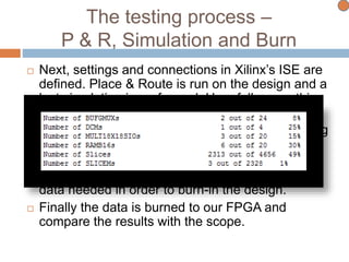
- Testing the design through simulation, synthesis, place and route, and finally programming the designed FPGA board.
- Verifying the results by comparing the functionality to the original 68HC12 microcontroller board.


![Package
Constants were defined.
When reading a file, words are far more
understandable then numbers.
Changes in vector size of signals used in various
locations are made only from the package.
Procedures were defined for better
organization.
Function for std_logic_vector-to-string[1].](https://image.slidesharecdn.com/855e3ee8-686f-412c-a60c-3d68240eefa8-160604190252/85/slide-14-320.jpg)


![Backup
In big projects, it is very important to backup all
our work, in case of data loss.
For that purpose a net service was used,
provided by assembla[2].
Each member of the project can update and
commit files of any kind to the project.
All sub-versions (SVN) are saved and stored
in-site.
All files can be easily compared to
previous versions in-site (diff).](https://image.slidesharecdn.com/855e3ee8-686f-412c-a60c-3d68240eefa8-160604190252/85/slide-26-320.jpg)


![Testing Programs –
Tiny Encryption Algorithm (TEA)
Receives a hex 8-byte
word for encryption.
Receives a hex 16-byte
key-word.
Offers to encrypt or
decrypt the given word
according to the key.
All is done using the UART.
No change was done to
the original algorithm[3].](https://image.slidesharecdn.com/855e3ee8-686f-412c-a60c-3d68240eefa8-160604190252/85/slide-44-320.jpg)
![Testing Programs –
RC4
Receives an ascii
word for encryption.
Receives an ascii key
word.
Offers to encrypt or
decrypt the given
word according to the
key.
All is done using the
UART.
No change was done
to the original
algorithm[4].](https://image.slidesharecdn.com/855e3ee8-686f-412c-a60c-3d68240eefa8-160604190252/85/slide-45-320.jpg)


![Bibliography
[1] http://www.edaboard.com/thread9311.html
[2] http://www.assembla.com/
[3]
http://en.wikipedia.org/wiki/Tiny_Encryption_Algorithm
[4] http://www.cypherspace.org/rsa/rc4c.html
[5] HC12 CPU12 Reference Manual.
[6] Han-Way Huang, MC68HC12: An Introduction,
Software and Hardware Interfacing, Mankato:
Thomson Delmar Learning, 2003.
[7] Digilent Romania, RS232 Reference Component,
[Online], July 2008, [July 2011], Available at:
http://www.digilentinc.com/Data/Documents/Referenc
e%20Designs/RS232%20RefComp.zip [Online], pdf](https://image.slidesharecdn.com/855e3ee8-686f-412c-a60c-3d68240eefa8-160604190252/85/slide-49-320.jpg)