Microprocessor 8086 notes
•Download as DOCX, PDF•
4 likes•691 views

Notes of Microprocessor provided by Prof.Sandeep Gulia sir NIET,Greater Noida

Recommended
More Related Content
What's hot
What's hot (20)
Viewers also liked
Similar to Microprocessor 8086 notes
Similar to Microprocessor 8086 notes (20)
More from Ravi Anand
More from Ravi Anand (20)
Recently uploaded
Recently uploaded (20)
Microprocessor 8086 notes
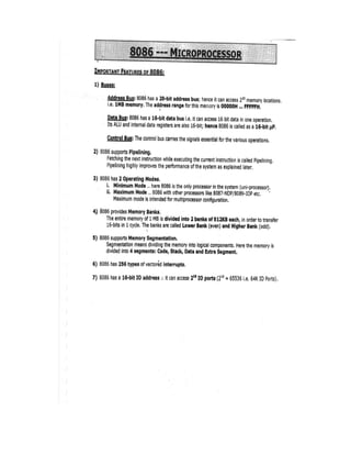
- 7. The memory address in 8086 space can be viewed as a sequence of one million bytes in which any byte may contain an 8-bit data element and any two consecutive bytes may contain a 16-bit data element. There is no constraint on byte or word address boundaries. The address space is physically connected to a 16-bit data bus by dividing the address space into two 8-bit banks of up to 512K bytes each. One bank is connected to the lower half of the 16-bit data bus (D0 – D7) and contains even address bytes. i.e., when A0 bit is low, the bank is selected. The other bank is connected to the upper half of the data bus (D8 - D15) and contains odd address bytes. i.e., when A0 is high and BHE (Bus High Enable) is low, the odd bank is selected. A specific byte within each bank is selected by address lines A1-A19.
- 8. Data can be accessed from the memory in four different ways. Theyare: 8 - bit data from Lower (Even) address Bank. 8 - bit data from Higher (Odd) address Bank. 16 - bit data starting from Even Address. 16 - bit data starting from Odd Address. 8-bit data from Even address Bank Odd B ank Even Bank x + 1 x + 3 x + 5 x x + 2 x + 4 A1-A19 D 0-D 15 BH E = 1 D 8 -D 15 D 0-D 7 Fig. 8-bit Data Access from Even Address A 0 = 0 To access memory bytes from Even address, information is transferred over the lower half of the data bus (D0 - D7). The A0 is output LOW and BHE is output HIGH enabling only the even address bank. Higher Address Bank (512K x 8) BHE ODD Lower Address Bank (512K x 8) A0 EVEN A1-A19 Address Bus D8-D15 D0-D7 Data Bus (D0 - D15)
- 9. Example: Consider loading a byte of data into CH register (higher order 8-bits of CX register) from the memory location with an even address. The data will be accessed from the even bank via the (D0 - D7) DATA BUS. Although this data is transferred into the 8086 over the lower 8-bit lines, the 8086 automatically redirects the data to the higher 8-bits of its internal 16- bit data path and hence to the CH-register. This capability allows bytes input-output transfer via the AL register to access I/O device connected to either the upper half of the data bus or the lower half of the 16-bit data bus. 8-bit Data from Odd Address Bank To access memory byte from an odd address information, is transferred over the higher half of the data bus (D8 - D15). The BHE output low enables the upper memory bank. A0 is output high to disable the lower memory bank. It is illustrated in fig. 7 O d d B a n k E v e n B a n k 16-bit Data Access starting from Even -Address Odd Bank Even Bank x + 1 x + 3 x x + 2 A1-A19 D0-D15 D8-D15 BHE =0 D0-D7 A0 = 0 16-bit data from an even address is accessed in a single bus cycle. Address lines A1 - A19 select the appropriate byte within each bank. A0 low and BHE low enables both banks simultaneously. 16-bit Data Access starting from Odd Address A 16-bits word located at an odd address (two consecutive bytes with the least significant byte at an odd byte address) is accessed using two bus cycles. During the first bus cycle the lower byte (with the odd address 0005 as shown in fig.) is accessed. x + 1 x + 3 x x + 2 B H E = 0 A 0 = 1 A 1 -A 1 9 D 0 - D7 D 8 - D 1 5 D 0 -D 1 5
- 10. 0005 0007 0009 0004 0006 0008 A1-A19 A1-A9 D0-D7 D8-D15 0005 0007 0009 0004 0006 0008 A1-A19 A1-A9 D0-D7 D8-D15 Odd Bank Even Bank Odd Bank Even Bank (a) First Access f rom Odd Address (b) Next Access f rom Ev en Address During the second bus cycle, the upper byte (with the even address 0006H) is accessed. During the first bus cycle, A1 - A19 address bus specifies the address and A0 as 1 and BHE is low. Therefore the even memory bank is disabled and odd memory bank is enabled. During the second bus cycle, the address is incremented. Therefore A0 is zero and BHE is made high. The even memory bank is enabled and the odd memory bank is disabled.