
Recommended
More Related Content
Similar to unit 3.pptx
Similar to unit 3.pptx (20)
Recently uploaded
Recently uploaded (20)
unit 3.pptx
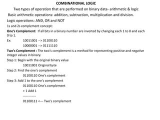
- 1. COMBINATIONAL LOGIC Two types of operation that are performed on binary data- arithmetic & logic Basic arithmetic operations: addition, subtraction, multiplication and division. Logic operations: AND, OR and NOT 1s and 2s complement concept: One‘s Complement: If all bits in a binary number are inverted by changing each 1 to 0 and each 0 to 1. Ex: 10011001 --> 01100110 10000001 --> 01111110 Two‘s Complement : The two‘s complement is a method for representing positive and negative integer values in binary. Step 1: Begin with the original binary value 10011001 Original byte Step 2: Find the one's complement 01100110 One's complement Step 3: Add 1 to the one's complement 01100110 One's complement + 1 Add 1 ------------ 01100111 <--- Two's complement
- 2. Basic Rules of Binary Addition and Subtraction: we can write the basic rules of binary addition as follows: 1. 0 + 0 = 0. 2. 0 + 1 = 1. 3. 1 + 0 = 1. 4. 1 + 1 = 0 with a carry of ‗1‘ to the next more significant bit. 5. 1 + 1 + 1 = 1 with a carry of ‗1‘ to the next more significant bit. The basic principles of binary subtraction include the following: 1. 0 - 0 = 0. 2. 1 - 0 = 1. 3. 1 - 1 = 0. 4. 0 - 1 = 1 with a borrow of 1 from the next more significant bit. Addition Using the 2‟s Complement: Subtraction of Larger-Bit Binary Numbers:
- 3. Subtraction of Larger-Bit Binary Numbers: The different steps to do subtraction in 2‘s complement: 1. Represent the minuend and subtrahend in 2‘s complement form. 2. Find the 2‘s complement of the subtrahend. 3. Add the 2‘s complement of the subtrahend to the minuend. 4. Disregard the final carry, if any. 5. The result is in 2‘s complement form. Sign-Bit Magnitude -In the sign-bit magnitude representation of positive and negative decimal numbers, the MSB represents the ‗sign‘, with a ‗0‘ denoting a plus sign and a ‗1‘ denoting a minus sign. -The remaining bits represent the magnitude. In eight-bit representation, while MSB represents the sign, the remaining seven bits represent the magnitude.
- 4. ADDER •HALF ADDER •FULL ADDER HALF ADDER-it is a logic circuit which add two binary bits and produce sum and carry as output LOGICAL EXPRESSION: SUM=A B CARRY=AB LOGIC CIRCUIT: SUM-An EX-OR gate is used to produce the output of sum. CARRY-An AND gate is used to produce the output of carry. TRUTH TABLE: WORKING: STEP:1-when the input A=0&B=0 the sum is 0 and the carry is 0. STEP:2-when the input A=0&B=1 the sum is 1 and the carry is 0. STEP:3-when the input A=1&B=0 the sum is 1 and the carry is 0. STEP:4-when the input A=1&B=1 the sum is 0 and the carry is 1. +
- 5. FULL ADDER- it is a logic circuit which add three inputs and produce sum and carry as outputs LOGICAL EXPRESSION: SUM=A B C CARRY=AB+BC+CA LOGIC CIRCUIT: SUM- EX-OR gate is used to produce the output of sum CARRY- Three AND & one OR gates are used to produce the output of carry. WORKING: STEP:1-when the input ABC=000 the sum is 0 and the carry is 0. STEP:2-when the input ABC=011 the sum is 0 and the carry is 1. STEP:3-when the input ABC=100 the sum is 1 and the carry is 0. STEP:4-when the input ABC=111 the sum is 1 and the carry is 1. + +
- 6. SUBTRACTOR HALF SUBTRACTOR FULL SUBTRACTOR HALF SUBTRACTOR-it is a logic circuit which subtract two binary bits and produce difference and borrow as outputs LOGICAL EXPRESSION: DIFFERENCE=A B BORROW= AB LOGIC CIRCUIT: DIFFERENCE-An EX-OR gate is used to produce the output of difference. BORROW-A NOT gate & an AND gate are used to produce the output of borrow. WORKING: STEP:1-when the input A=0&B=0 the Difference is 0 and the Borrow is 0. STEP:2-when the input A=0&B=1 the Difference is 1 and the Borrow is 1. STEP:3-when the input A=1&B=0 the Difference is 1 and the Borrow is 0. STEP:4-when the input A=1&B=1 the Difference is 0 and the Borrow is 0. TRUTH TABLE: +
- 7. FULL SUBTRACTOR- it is a logic circuit which subtract three inputs and produce Difference and Borrow as outputs LOGICAL EXPRESSION: SUM=A B C CARRY= AB+BC+CA LOGIC CIRCUIT: DIFFERENCE- An EX-OR gate is used to produce the output of difference BORROW- A NOT gate, Three AND & one OR gates are used to produce the output of borrow. WORKING: STEP:1-when the input ABC=000 the Difference is 0 and the Borrow is 0. STEP:2-when the input ABC=010 the Difference is 1 and the Borrow is 1. STEP:3-when the input ABC=100 the Difference is 1 and the Borrow is 0. STEP:4-when the input ABC=111 the Difference is 0 and the Borrow is 0. TRUTH TABLE: + +
- 8. PARITY GENERATOR AND CHECKER PARITY BIT-It is a binary bit [0&1]used to find the error in digital data transmission and reception. PARITY GENERATOR: -It is logic circuit used to generate the parity bit. -it is provided at the transmitter side. Types: even parity generator odd parity generator
- 9. Even Parity Generator -EX-OR gate is used as a parity generator. -EX-OR gate will produce the output as 1 when the inputs are complement or odd. -EX-OR gate will produce the output as 0 when the inputs are same or even. -let the input is 00110001, it is an odd parity. - now the output of EX-OR gate is 1. - this bit has been added with original data, becomes 100110001. - now the odd parity converted as even parity.
- 10. Odd Parity Generator -EX-OR and NOT gates are used as in parity generator. -EX-OR gate will produce the output as 1 when the inputs are complement or odd. -EX-OR gate will produce the output as 0 when the inputs are same or even. - NOT gate will complement the input. -let the input is 00100001, it is an odd parity. - now the output of EX-OR gate is 0. - then the NOT gate complement the 0 as 1 - this bit has been added with original data, becomes 100100001. - now the even parity converted as odd parity.
- 11. PARITY CHECKER: -IT is a logic circuit used to check the parity bit at the receiver side. -EX-OR gates are used in parity checker circuit. -EX-OR gate will produce the output as 1 when the inputs are complement or odd. -EX-OR gate will produce the output as 0 when the inputs are same or even. WORKING: -when the input is even parity the checker will produce the output as 0. -when the input is odd parity the checker will produce the output as 1. -let the input is 01010 the checker will produce the output as 0. -let the input is 01110 the checker will produce the output as 1.
- 12. DIGITAL COMPARATOR -It is combinational logic circuit which compare the two inputs and produce three different outputs. -An EX-OR gate is the basic comparator element. -AND gate & NOT gates also used in the comparator circuit. - the comparator can produce three different outputs. Such as, -A<B -A=B -A>B
- 13. LOGICAL DIAGRAM: - A NOT & AND gate will produce the output of A>B. - Another NOT & AND gate will produce the output of A<B. - An EX-OR gate will produce the output of A=B. WORKING: - When the input AB=00 the output A=B is 1 and remains o. - When the input AB=01 the output A<B is 1 and remains o. - When the input AB=10 the output A>B is 1 and remains o. - When the input AB=11 the output A=B is 1 and remains o.
- 14. ARITHMETIC LOGIC UNIT “It is combinational logic circuit which perform arithmetic and logical operations” The arithmetic operations performed by ALU are, Addition, Subtraction, Multiplication & Division The logical operations performed by ALU are, NOT,AND,OR &EX-OR BLOCK DIAGRAM OF ALU: S0,S1,S2-mode selection lines which is used to select the mode of operation. A0,A1,A2,A3 and B0,B1,B2,B3 -input lines used to give binary inputs to the ALU. Y0,Y1,Y2,Y3 -output lines used to produce the 4-bit output. Cin-carry input which is used to give carry input. Cout-carryoutput which is used to produce carry output.
- 15. TRUTH TABLE: WORKING: - for performing arithmetic operations, the set S2 line as 0. in which -set 0010 for addition operation - set 0100 for subtraction operation - set 0110 for multiplication operation - set 0111 for division operation - for performing logical operations, the set S2 line as 1. in which -set 100 for OR operation - set 101 for AND operation - set 110 for EX-OR operation - set 111 for NOT operation
- 16. EN CODER “ it is a combinational logic circuit which converts an active input signal into binary coded output signal” “ it is like multiplexer, the output lines less than number of input lines” - it has 10 input lines and 4 output lines. - 10 push type switches are used. - 4 OR gates are used. LOGIC DIAGRAM: -it has 10 input lines(0-9) and four output lines(A-D) -the input lines are connected with push type switches -this switches are connected with OR gates based on the truth table - These 4 OR gate will produce the output of ABCD. 0101.
- 17. WORKING: -any input line pressed, the corresponding OR gate will produce the output as 1. for example, - 5th line pressed, the A & C gate produce the output as 1. - then the remaining B & D gates produce the output as 0. - now the output of encoder is 0101. - hence, the decimal number 5 converted into binary code
- 18. DECODER “ it is like demultiplexer, the output lines more than input lines” “ any one of the output line is selected at a time based on the applied input lines” - it has 3 input lines and 8 output lines. - 3 NOT gates are used to generate the output of A,B,C. - 8 AND gates are used to generate the output of Y0-Y7. LOGIC DIAGRAM: - the input lines ABC connected with NOT gate which produce the output of ABC. -these input lines are connected with AND gate based on the truth table. - these AND gates will produce the output of y0,y1,y2,y3,y4,y5,y6 & y7.
- 19. WORKING: For example, -when CBA=000, all the inputs of 0th AND gate is 1, then the output Y0=1 and remain 0. -when CBA=011, all the inputs of 3rd AND gate is 1, then the output Y0=1 and remain 0. -when CBA=101, all the inputs of 6th AND gate is 1, then the output Y0=1 and remain 0. -when CBA=111, all the inputs of 7th AND gate is 1, then the output Y0=1 and remain 0.
- 20. BCD TO 7 SEGMANT DECODER “ it is one type of decoder which can display the digits from 0 to 9” -it has less inputs and more outputs, hence it is one type of decoder. -by controlling the current flow through the LED we can display the desired character . -it has 4 BCD input lines[ABCD] and 8 output lines[abcdefg]. LOGIC DIAGRAM: - there are 4 NOT, 10 AND, 7 OR & 7 LED’s used to develop the circuit. - 4 NOT gates are used to get the complement inputs A B C D. - 10 AND gates are used to generate the outputs P0,P1,P2,P3,P4,P5,P6,P7,P8 & P9. - all the and gates are 4 input gates and it is given based on the truth table. - 4 OR gates are used to produce the output of a,b,c,d,e,f, & g. - all the inputs of OR gates are given by the truth table. - the output of OR gates are connected with corresponding LED’s directly.
- 22. WORKING PRINCIPLE: ‘ Among the ten AND gates only one is enabled at a time, remains 0’ -when the input DCBA=0001, which makes all the input of gate 1 is 1. -then the output P1 is 1 and remaining AND gates outputs are 0. -the P1 makes the B and C OR gates are high. -hence the segments b & c goes to high and remains low. -which display the digit 1, it is equivalent of binary input 0001. Similarly, -when DCBA=1000 the ABCDEF OR gates are high which display 8. - when DCBA=1001 the ABCDFG OR gates are high which display 9.
- 23. MULTIPLEXER " it is data selector with more number of inputs and produce only one output" "which select any one of input lines based on the selection lines - it has 8 input lines and only one output line. - it has 3 selection lines used to select the input. LOGICAL DIAGRAM: - by using selection lines we can create 8 combinations - 3 NOT gates are used to produce the output A B C - 8 AND gates are used to generate 8 different outputs - all the and gates are 4 input gates - input to the AND gate is given by the truth table - the input lines D0,D1,D2,D3,D4,D5,D6& D7 directly given to the AND gates. - an OR gate is used to add all the outputs of AND gates and produce the output Y.
- 24. WORKING: LOGICAL DIAGRAM: -let the selection lines input A2A1A0=000, the 0th AND gate willproduce the input D0 to the output . - when the input D0 is 0, the output Y=0 - when the input D0 is 1, the output Y=1 Similarly, -let the selection lines input A2A1A0=010, the 2nd AND gate will produce the input D2 to the output . -let the selection lines input A2A1A0=101, the 5th AND gate will produce the input D5 to the output . -let the selection lines input A2A1A0=111, the 7th AND gate will produce the input D7 to the output . TRUTH TABLE:
- 25. DEMULTIPLEXER " it is data distributor with only one input and produce more number of output" "which produce any one of the input line at the output side based on the selection lines“ - it has only one input line[D] and output 8 lines [Y0,Y1,Y2,Y3,Y4,Y5,Y6,Y7]. - it has 3 selection lines[s0,s1,s2] used to select the input. LOGICAL DIAGRAM: - by using selection lines we can create 8 combinations - 3 NOT gates are used to produce the output A B C - 8 AND gates are used to generate 8 different outputs - all the and gates are 4 input gates - input to the AND gate is given by the truth table - the input line D is combined with selection lines, then fed into AND gate. - these AND gates will produce the output Y0,Y1,Y2,Y3,Y4,Y5,Y6,Y7
- 26. WORKING: LOGICAL DIAGRAM: - let the selection line inputs A2A1A0=000, the 0th AND gate will produce the input D as the output, then remains 0. - when the input D is 0, the output Y0=0 - when the input D is 1, the output Y0=1 Similarly, - let the selection lines input A2A1A0=010, the 2nd AND gate will produce the input D as the output, then remains 0. - let the selection lines input A2A1A0=101, the 5th AND gate will produce the input D5 to the output, then remains 0. - let the selection lines input A2A1A0=111, the 7th AND gate will produce the input D7 to the output, then remains 0. TRUTH TABLE:
- 27. DIGITAL LOGIC FAMILIES: A group of Ics with same supply voltages used for performing various logic functions. Types : i) unipolar-(PMOS,NMOS) ii) bipolar-(CMOS) 1) saturated transistors - TTL, DTL.I2L 2) non saturated transistors – CMOS Characteristics of digital ICs 1. Speed of operation 2. Power dissipation 3. Fan in 4. Fan out 5. Noise immunity 6. Package density 1.speed of operation or propagation delay The time difference between the application of input and appearance of output is called as propagation delay 2. Power dissipation Power dissipation is the nature of the power consumed by a logic gate when fully driven by all its inputs,it is expressed in milliwatts. 3. Fan in The number of inputs connected to a gate is known as fan in of the gate. 5. Fan out The maximum number of standard logic inputs that an output can drive reliably 6. Noise immunity The circuit ability to tolerate noise without causing spurious changes in the output voltage is called noise immunity. 7. Packaged density The number of devices that can be fabricated per unit area of a chip is called packaged density.
- 28. Transistor-transistor logic (TTL logic): -The basic TTL logic circuit is NAND gate shown in figure. -Q 1 is a multiple- emitter input transistor contains two emitter terminals.Each emitter acts like a diode.The overall circuit acts like a 2 input NAND gate. -The output transistors Q3 and Q4 are connected in a totem pole arrangement(ie one npn transistor isconnected in series with the another npn transistor.) Working: -With the totem pole connection,either Q3 or Q4 is on.When Q3 is on, the output is high. When Q4 is on, the output is low. -The input voltages A and B are either low or high. -If A or B is low, the base of voltage of Q1 is reduced which inturn reduces thebase voltage of Q2. So , Q2 is in cut off. -Due to Q2 open, Q4 goes into cut off.Now the base voltage of Q3 goes high. Q3 act as a emitter follower. The output becomes high. -If A and B are both high , the emitter diodes of D1 stop conducting and thecollector diode goes into forward conduction. This forces the base voltage of Q2 to high . It increases the saturation of Q4.
- 29. CMOS LOGIC (complementary metal oxide semiconductor logic): CMOS NAND gate consists of one N channel and P channel device connected in push-pull operation. Because of push-pull operation, one device is normally on and the other is normally off. Q1 and Q2 form one complementary connection and Q3 and Q4 form another connection shown figure. Working: If A= low,it will close Q1 and open Q2 A= high,it will open Q1 and close Q2 B=low ,it will open Q3 and close Q4 B=high,it will close Q3 and open Q4 Operation Case 1 A=0 and B=0, now Q1 is closed and output goes high. Case 2 A=0 and B=1,Since Ais low, Q1 is closed and the output is high. Case 3 A=1 and B=0, now Q4 is closed and output goes high Case4 A=1 and B=1,Since Ais low, Q1 is closed and the output is low. When the inputs are high, Q2 and Q3 are closed pulling the output to the ground.